

Page 1
General Description
The MAX4249–MAX4257 low-noise, low-distortion operational amplifiers offer rail-to-rail outputs and singlesupply operation down to 2.4V. They draw 400µA of
quiescent supply current per amplifier while featuring
ultra-low distortion (0.0002% THD), as well as low input
voltage-noise density (7.9nV/√Hz) and low input
current-noise density (0.5fA/√Hz). These features make
the devices an ideal choice for portable/battery-powered
applications that require low distortion and/or low noise.
For additional power conservation, the MAX4249/
MAX4251/MAX4253/MAX4256 offer a low-power shutdown mode that reduces supply current to 0.5µA and
puts the amplifiers’ outputs into a high-impedance
state. The MAX4249-MAX4257’s outputs swing rail-torail and their input common-mode voltage range
includes ground. The MAX4250–MAX4254 are unitygain stable with a gain-bandwidth product of 3MHz.
The MAX4249/MAX4255/MAX4256/MAX4257 are internally compensated for gains of 10V/V or greater with a
gain-bandwidth product of 22MHz. The single MAX4250/
MAX4255 are available in space-saving 5-pin SOT23
packages. The MAX4252 is available in an 8-bump chipscale package (UCSP™) and the MAX4253 is available in
a 10-bump UCSP. The MAX4250AAUK comes in a 5-pin
SOT23 package and is specified for operation over the
automotive (-40°C to +125°C) temperature range.
Applications
Wireless Communications Devices
PA Control
Portable/Battery-Powered Equipment
Medical Instrumentation
ADC Buffers
Digital Scales/Strain Gauges
Features
o Available in Space-Saving UCSP, SOT23, and
µMAX®Packages
o Low Distortion: 0.0002% THD (1kΩ load)
o 400µA Quiescent Supply Current per Amplifier
o Single-Supply Operation from 2.4V to 5.5V
o Input Common-Mode Voltage Range Includes
Ground
o Outputs Swing Within 8mV of Rails with a 10kΩ
Load
o 3MHz GBW Product, Unity-Gain Stable
(MAX4250–MAX4254)
22MHz GBW Product, Stable with A
V
≥ 10V/V
(MAX4249/MAX4255/MAX4256/MAX4257)
o Excellent DC Characteristics
VOS= 70µV
I
BIAS
= 1pA
Large-Signal Voltage Gain = 116dB
o Low-Power Shutdown Mode
Reduces Supply Current to 0.5µA
Places Outputs in a High-Impedance State
o 400pF Capacitive-Load Handling Capability
MAX4249–MAX4257
UCSP, Single-Supply, Low-Noise,
Low-Distortion, Rail-to-Rail Op Amps
________________________________________________________________
Maxim Integrated Products
1
19-1295; Rev 8; 10/11
For pricing, delivery, and ordering information, please contact Maxim Direct at 1-888-629-4642,
or visit Maxim’s website at www.maxim-ic.com.
Ordering Information continued at end of data sheet.
Selector Guide appears at end of data sheet.
UCSP is a trademark and µMAX is a registered trademark of Maxim Integrated Products, Inc.
Pin/Bump Configurations continued at end of data sheet.
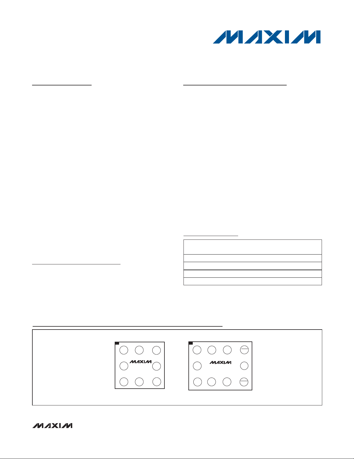
Pin/Bump Configurations
Ordering Information
+
Denotes a lead(Pb)-free/RoHS-compliant package.
T = Tape and reel.
PART TEMP RANGE
MAX4249ESD+
MAX4249EUB+ -40°C to +85°C 10 µMAX —
MAX4250EUK+T
M AX 4250AAU K+ T- 40°C to + 125°C 5 SOT23 AEYJ
-40°C to +85°C 14 SO —
-40°C to +85°C 5 SOT23 ACCI
PINPACKAGE
MARK
TOP
TOP VIEW
(BUMPS ON BOTTOM)
12 3
V
OUTA
A
B
C
INA-
INA+
DD
MAX4252
V
SS
UCSP
OUTB
INB-
INB+
OUTB
V
OUTA
A4
A3
A2
A1
INB+
INA+
SHDNB
V
C4
SHDNA
B4
SS
INB-
B1
DD
MAX4253
C2 C3
C1
INA-
UCSP
Page 2
MAX4249–MAX4257
UCSP, Single-Supply, Low-Noise,
Low-Distortion, Rail-to-Rail Op Amps
2 _______________________________________________________________________________________
ABSOLUTE MAXIMUM RATINGS
ELECTRICAL CHARACTERISTICS
(VDD= 5V, VSS= 0V, VCM= 0V, V
OUT
= VDD/2, RLconnected to VDD/2, SHDN = VDD, TA= T
MIN
to T
MAX
, unless otherwise noted.
Typical values are at T
A
= +25°C.) (Notes 2, 3)
Stresses beyond those listed under “Absolute Maximum Ratings” may cause permanent damage to the device. These are stress ratings only, and functional
operation of the device at these or any other conditions beyond those indicated in the operational sections of the specifications is not implied. Exposure to
absolute maximum rating conditions for extended periods may affect device reliability.
Power-Supply Voltage (VDDto VSS) ......................+6.0V to -0.3V
Analog Input Voltage (IN_+, IN_-)....(V
DD
+ 0.3V) to (VSS- 0.3V)
SHDN Input Voltage ......................................6.0V to (V
SS
- 0.3V)
Output Short-Circuit Duration to Either Supply ..........Continuous
Continuous Power Dissipation (T
A
= +70°C)
5-Pin SOT23 (derate 7.1mW/°C above +70°C)...........571mW
8-Bump UCSP (derate 4.7mW/°C above +70°C)........379mW
8-Pin µMAX (derate 4.5mW/°C above +70°C) ............362mW
8-Pin SO (derate 5.88mW/°C above +70°C)...............471mW
10-Bump UCSP (derate 6.1mW/°C above +70°C) ......484mW
10-Pin µMAX (derate 5.6mW/°C above +70°C) ...........444mW
14-Pin SO (derate 8.33mW/°C above +70°C)..............667mW
Operating Temperature Range ...........................-40°C to +85°C
MAX4250AAUK .............................................-40°C to +125°C
Junction Temperature......................................................+150°C
Storage Temperature Range .............................-65°C to +150°C
Lead Temperature (soldering, 10s) .................................+300°C
Soldering Temperature (reflow) .......................................+260°C
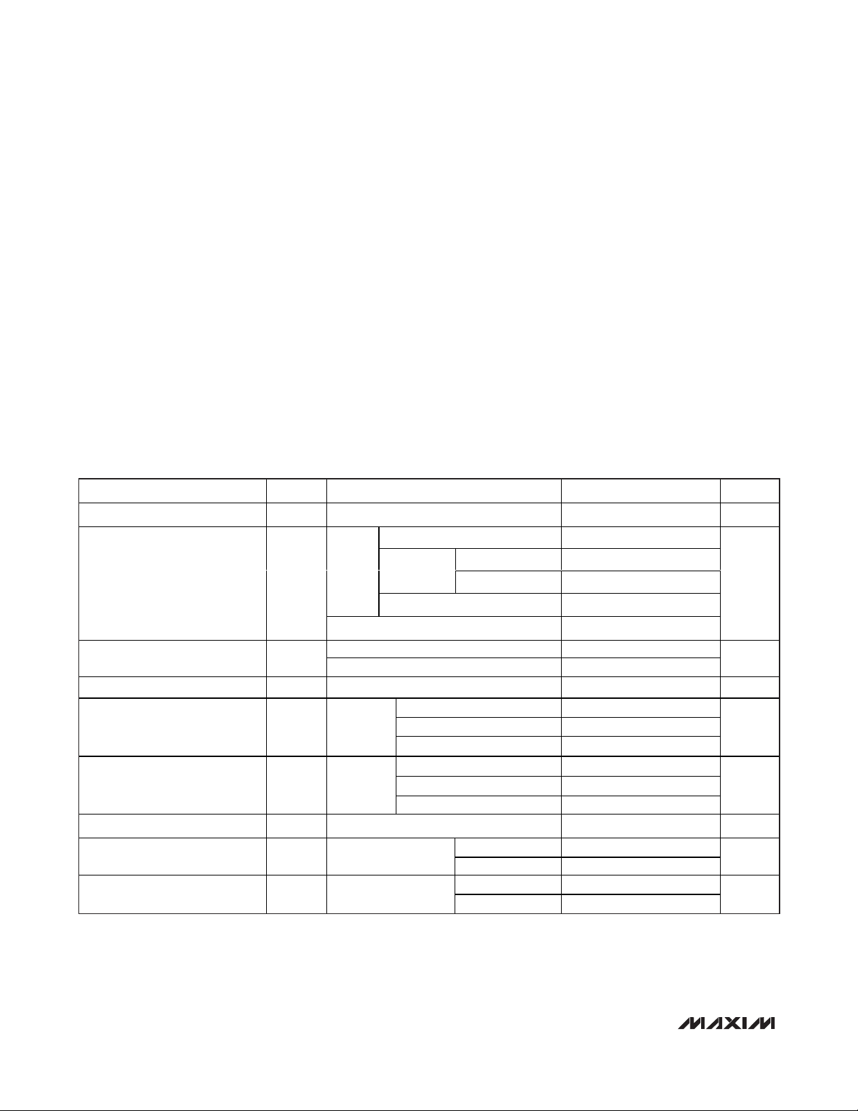
PARAMETER SYMBOL CONDITIONS MIN TYP MAX UNITS
Supply Voltage Range V
Quiescent Supply Current Per
Amplifier
Input Offset Voltage (Note 5) V
Input Offset Voltage Tempco TCV
Input Offset Current I
Differential Input Resistance R
Input Common-Mode Voltage
Range
Common-Mode Rejection Ratio CMRR
DD
I
Q
OS
OS
B
OS
IN
V
CM
(Note 4) 2.4 5.5 V
VDD = 3V 400
Normal
mode
Shutdown mode (SHDN = VSS) (Note 2) 0.5 1.5
E temperature ±0.07 ±0.75
MAX4250AAUK ±1.85
(Note 6)
(Note 6)
Guaranteed by
CMRR test
V
SS
V
DD
VDD = 5V
V
= 5V, UCSP only 420 655
DD
TA = +25°C 0.1 1
TA = -40°C to +85°C 50Input Bias Current I
T
= -40°C to +125°C 1500
A
TA = +25°C 0.1 1
TA = -40°C to +85°C 10
T
= -40°C to +125°C 100
A
- 0.2V ≤ VCM ≤
- 1.1V
E temperature 420 575
MAX4250AAUK 675
0.3 µV/°C
1000 GΩ
E temperature -0.2 V
MAX4250AAUK 0 V
E temperature 70 115
MAX4250AAUK 68
DD
DD
mV
-1.1
-1.1
µA
pA
pA
V
dB
Page 3
MAX4249–MAX4257
UCSP, Single-Supply, Low-Noise,
Low-Distortion, Rail-to-Rail Op Amps
_______________________________________________________________________________________ 3
ELECTRICAL CHARACTERISTICS (continued)
(VDD= 5V, VSS= 0V, VCM= 0V, V
OUT
= VDD/2, RLconnected to VDD/2, SHDN = VDD, TA= T
MIN
to T
MAX
, unless otherwise noted.
Typical values are at T
A
= +25°C.) (Notes 2, 3)
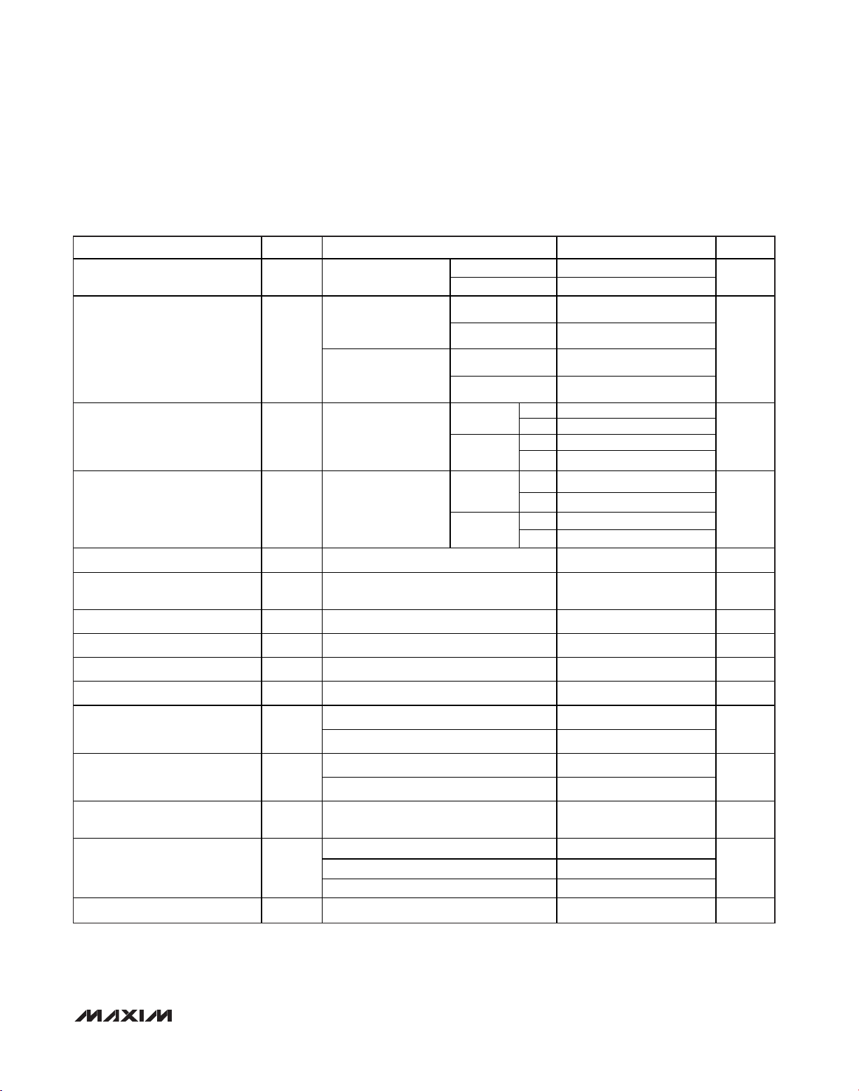
PARAMETER SYMBOL CONDITIONS MIN TYP MAX UNITS
Power-Supply Rejection Ratio PSRR VDD – 2.4V to 5.5V
Large-Signal Voltage Gain A
Output Voltage Swing V
Output Voltage Swing V
Output Short-Circuit Current I
Output Leakage Current I
SHDN Logic Low V
SHDN Logic High V
SHDN Input Current IIL/I
Input Capacitance 11 pF
E temperature 75 100
MAX4250AAUK 72
= 10kΩ to V
V
OUT
OUT
SC
LEAK
IL
IH
R
L
= 25mV to V
V
OUT
– 4.97V
= 1kΩ to V
R
L
= 150V to V
V
OUT
– 4.75V
- V
|V
IN+
R
|V
R
IN-
= 10kΩ to V
L
- V
IN+
IN-
= 1kΩ to VDD/2
L
Shutdown mode (SHDN = VSS),
= V
V
OUT
SS
(Note 2) 0.2 X V
(Note 2) 0.8 X V
SHDN = VSS = VDD (Note 2) 0.5 1.5 µA
IH
/2;
DD
/2;
DD
DD
| ≥ 10mV;
/2
DD
| ≥ 10mV,
to V
DD
E temperature 80 116
DD
MAX4250AAUK 77
E temperature 80 112
MAX4250AAUK 77
VDD - V
OH
- V
V
OL
SS
VDD - V
OH
- V
V
OL
SS
(Note 2)
E825
A30
E720
A25
E 77 200
A 225
E 47 100
A 125
68 mA
0.001 1.0 µA
D D
DD
dB
dB
mV
mV
V
V
Gain-Bandwidth Product GBW
Slew Rate SR
Peak-to-Peak Input-Noise
Voltage
Input Voltage-Noise Density e
Input Current-Noise Density i
e
n
P-P
n
n
MAX4250–MAX4254
MAX4249/MAX4255/MAX4256/MAX4257
MAX4250–MAX4254
MAX4249/MAX4255/MAX4256/MAX4257
f = 0.1Hz to 10Hz
f = 10Hz
f = 1kHz
f = 30kHz
f = 1kHz
3
MHz
22
0.3
V/µs
2.1
760 nV
P-P
27
8.9
nV/√Hz
7.9
0.5 fA/√Hz
Page 4
MAX4249–MAX4257
UCSP, Single-Supply, Low-Noise,
Low-Distortion, Rail-to-Rail Op Amps
4 _______________________________________________________________________________________
ELECTRICAL CHARACTERISTICS (continued)
(VDD= 5V, VSS= 0V, VCM= 0V, V
OUT
= VDD/2, RLconnected to VDD/2, SHDN = VDD, TA= T
MIN
to T
MAX
, unless otherwise noted.
Typical values are at T
A
= +25°C.) (Notes 2, 3)
Note 2: SHDN is available on the MAX4249/MAX4251/MAX4253/MAX4256 only.
Note 3: All device specifications are 100% tested at T
A
= +25°C. Limits over temperature are guaranteed by design.
Note 4: Guaranteed by the PSRR test.
Note 5: Offset voltage prior to reflow on the UCSP.
Note 6: Guaranteed by design.
Note 7: Lowpass-filter bandwidth is 22kHz for f = 1kHz and 80kHz for f = 20kHz. Noise floor of test equipment = 10nV/√Hz.
PARAMETER SYMBOL CONDITIONS MIN TYP MAX UNITS
Total Harmonic Distortion Plus
Noise
Capacitive-Load Stability
Gain Margin GM
Phase Margin ΦM
Settling Time
THD+N
MAX4250–MAX4254
A
= 1V/V, V
V
= 1kΩ to GND
R
L
(Note 7)
MAX4249/MAX4255/
MAX4256/MAX4257
A
= 1V/V, V
V
R
= 1kΩ to GND (Note 7)
L
No sustained oscillations
MAX4250–MAX4254, AV = 1V/V 10
MAX4249/MAX4255/MAX4256/MAX4257,
= 10V/V
A
V
MAX4250–MAX4254, AV = 1V/V 74
MAX4249/MAX4255/MAX4256/MAX4257,
= 10V/V
A
V
To 0.01%,
= 2V step
V
= 2V
OUT
= 2V
OUT
MAX4250–MAX4254 6.7
OUT
MAX4249/MAX4255/
MAX4256/MAX4257
P-P
P-P
,
,
f = 1kHz
f = 20kHz
f = 1kHz
f = 20kHz
0.0004
0.006
0.0012
0.007
400 pF
12.5
68
1.6
%
dB
Degrees
µs
I
Delay Time to Shutdown t
Delay Time to Enable t
Power-Up Delay Time t
SH
EN
PU
VDD = 5% of
normal
operation
V
OUT = 2.5V,
V
OUT settles to
0.1%
V
DD = 0 to 5V step, VOUT stable to 0.1%
MAX4251/MAX4253 0.8
MAX4249/MAX4256 1.2
MAX4251/MAX4253 8
MAX4249/MAX4256 3.5
6µs
µs
µs
Page 5
MAX4249–MAX4257
UCSP, Single-Supply, Low-Noise,
Low-Distortion, Rail-to-Rail Op Amps
_______________________________________________________________________________________
5
0
10
5
20
15
25
30
35
40
-95
-55
-35
-75
-13
7
284969
90
110
131
152
172
192
MAX4251/MAX4256
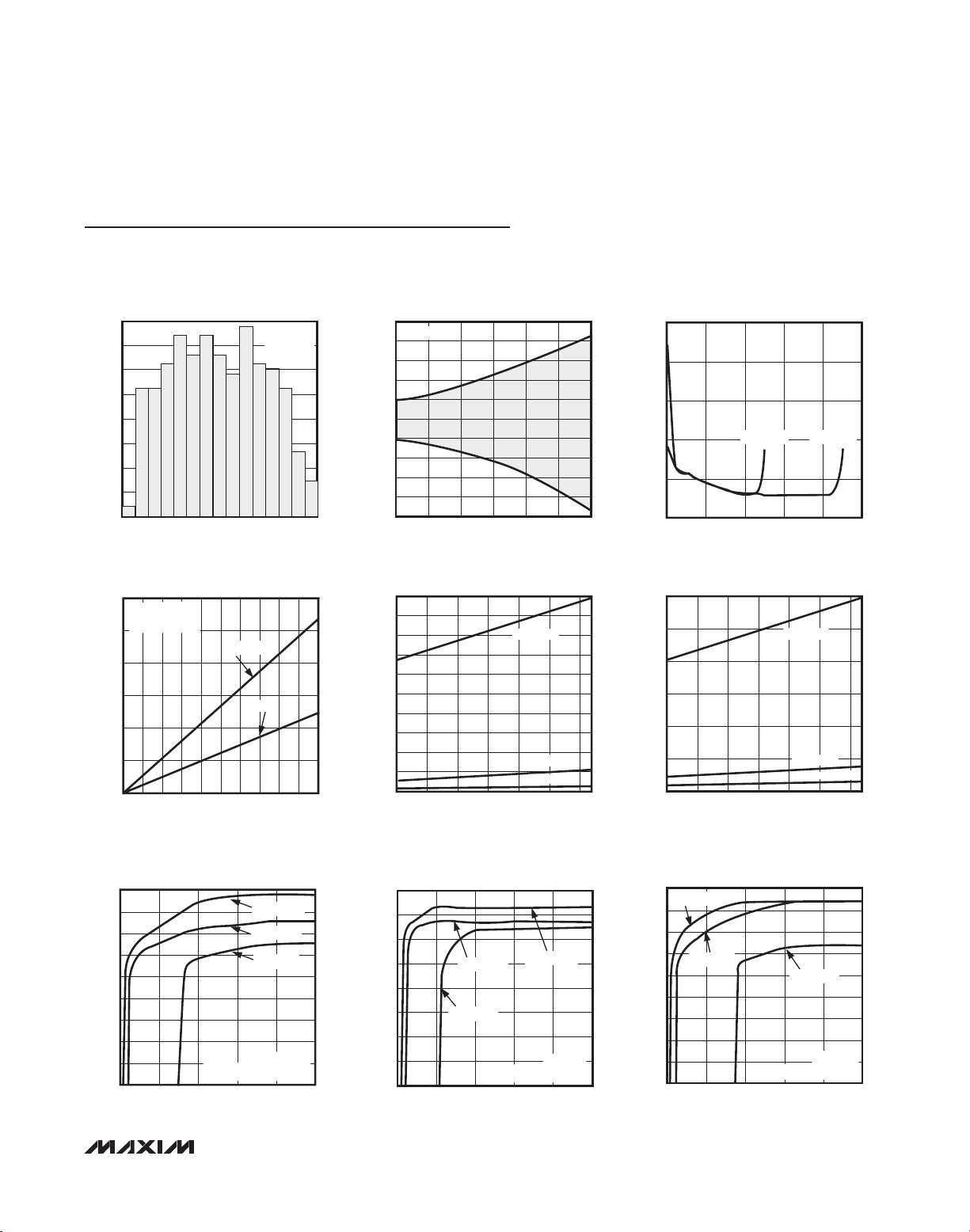
INPUT OFFSET VOLTAGE DISTRIBUTION
MAX4249-57 TOC01
VOS (µV)
NUMBER OF UNITS
400 UNITS
V
CM
= 0
T
A
= +25°C
Typical Operating Characteristics
(VDD= 5V, VSS= 0V, VCM= V
OUT
= VDD/2, input noise floor of test equipment =10nV/√Hz for all distortion measurements,
T
A
= +25°C, unless otherwise noted.)
OUTPUT VOLTAGE
0.6
0.5
0.4
0.3
0.2
OUTPUT VOLTAGE (V)
0.1
vs. OUTPUT LOAD CURRENT
VDD = 3V OR 5V
= ±10mV
V
DIFF
VDD - V
OH
V
OL
0
04312 5678910
OUTPUT LOAD CURRENT (mA)
MAX4249-57 TOC04
OFFSET VOLTAGE
vs. TEMPERATURE
250
VCM = 0
200
150
100
50
(µV)
0
OS
V
-50
-100
-150
-200
-250
-40 0-20 20 40 60 80
TEMPERATURE (°C)
OUTPUT VOLTAGE SWING (VOH)
0.10
0.09
0.08
0.07
(V)
0.06
OH
- V
0.05
DD
V
0.04
0.03
0.02
0.01
0
-40 0-20 20 6040 80
vs. TEMPERATURE
RL = 1kΩ
RL = 10kΩ
TEMPERATURE (°C)
R
= 100kΩ
L
MAX4249-57 TOC02
MAX4249-57 TOC05
200
150
100
50
INPUT OFFSET VOLTAGE (µV)
0
-50
0.06
0.05
0.04
(V)
OL
0.03
V
0.02
0.01
0
INPUT OFFSET VOLTAGE
vs. INPUT COMMON-MODE VOLTAGE
VDD = 3V VDD = 5V
-0.5 1.50.5 2.5 3.5 4.5
INPUT COMMON-MODE VOLTAGE (V)
OUTPUT VOLTAGE SWING (VOL)
vs. TEMPERATURE
R
= 1kΩ
L
RL = 10kΩ
R
-40 0-20 20 6040 80
TEMPERATURE (°C)
= 100kΩ
L
MAX4249-57 TOC03
MAX4249 -57TOC06
LARGE-SIGNAL VOLTAGE GAIN
vs. OUTPUT VOLTAGE SWING
140
130
120
110
(dB)
100
V
A
90
80
70
60
50
0 10050 150 200 250
V
SWING FROM EITHER SUPPLY (mV)
OUT
LARGE-SIGNAL VOLTAGE GAIN
vs. OUTPUT VOLTAGE SWING
R
= 200kΩ
L
= 20kΩ
R
L
90
80
70
60
50
0 10050 150 200 250
V
OUT
R
REFERENCED TO GND
L
SWING FROM EITHER SUPPLY (mV)
R
REFERENCED TO GND
L
= 200kΩ
R
L
R
= 20kΩ
L
RL = 2kΩ
VDD = 3V
MAX4249-57 TOC07
LARGE-SIGNAL VOLTAGE GAIN
vs. OUTPUT VOLTAGE SWING
140
130
120
110
(dB)
V
A
100
90
80
70
60
0 50 100 150 200 250
V
OUT
= 20kΩ
R
L
R
= 2kΩ
L
SWING FROM EITHER SUPPLY (mV)
R
R
REFERENCED TO GND
L
= 200kΩ
L
VDD = 3V
MAX4249-57 TOC08
(dB)
A
140
130
120
110
V
100
R
= 2kΩ
L
MAX4249-57 TOC09
VDD = 5V
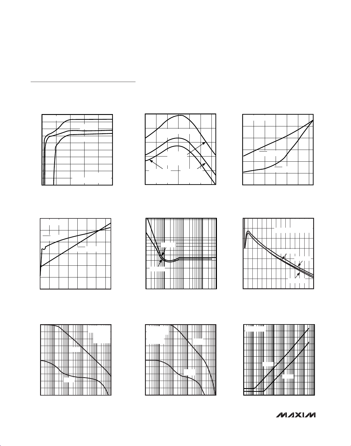
Page 6
MAX4249–MAX4257
UCSP, Single-Supply, Low-Noise,
Low-Distortion, Rail-to-Rail Op Amps
6 _______________________________________________________________________________________
50
80
70
60
90
100
110
120
130
140
150
0 10050 150 200 250
MAX4249-57 TOC10
VDD = 5V
R
L
REFERENCED TO GND
LARGE-SIGNAL VOLTAGE GAIN
vs. OUTPUT VOLTAGE SWING
V
OUT
SWING FROM EITHER SUPPLY (mV)
RL = 2kΩ
R
L
= 20kΩ
R
L
= 200kΩ
A
V
(dB)
100
110
105
115
120
125
-40 0-20 20 6040 80
LARGE-SIGNAL VOLTAGE GAIN
vs. TEMPERATURE
MAX4249-57 TOC11
TEMPERATURE (°C)
RL REFERENCED TO VDD/2
V
DD
= 5V
A
V
(dB)
RL = 1kΩ
V
OUT
= 150mV
TO 4.75mV
R
L
= 100kΩ
V
OUT
= 10mV
TO 4.99mV
R
L
= 10kΩ
V
OUT
= 20mV
TO 4.975mV
0.373
0.374
0.375
0.376
340
380
360
400
420
440
460
-40 0-20 20 6040 80
SUPPLY CURRENT AND SHUTDOWN
SUPPLY CURRENT vs. TEMPERATURE
MAX4249-57 TOC12
TEMPERATURE (°C)
SHUTDOWN SUPPLY CURRENT (µA)
PER AMPLIFIER
SHDN = V
DD
SUPPLY CURRENT (µA)
SHDN = V
SS
320
340
360
380
400
420
440
0
0.1
0.2
0.3
0.4
0.5
0.6
1.8 2.82.3 3.3 3.8 4.3 4.8 5.3 5.5
SUPPLY CURRENT AND SHUTDOWN
SUPPLY CURRENT vs. SUPPLY VOLTAGE
MAX4249-57 TOC13
SUPPLY VOLTAGE (V)
SUPPLY CURRENT (µA)
SHUTDOWN SUPPLY CURRENT (µA)
PER AMPLIFIER
SHDN = V
DD
SHDN = V
SS
2000
100
0.001 0.1 10.01 5
SUPPLY CURRENT
vs. OUTPUT VOLTAGE
MAX4249-57 TOC14
OUTPUT VOLTAGE (V)
SUPPLY CURRENT (µA)
1000
400
VDD = 5V
VDD = 3V
60
-40
100 10k 100k 1M1k 10M
MAX4250–MAX4254
GAIN AND PHASE vs. FREQUENCY
-20
-10
0
-30
MAX4249-57 TOC16
GAIN (dB)
PHASE (DEGREES)
10
20
30
40
50
180
-180
-108
-72
-36
-144
0
36
72
108
144
GAIN
PHASE
VDD = 3V, 5V
R
L
= 50kΩ
C
L
= 20pF
A
V
= 1000
0
-100
-110
1 1k 10k 100k 1M10 100 10M
MAX4250–MAX4254
POWER-SUPPLY REJECTION RATIO
vs. FREQUENCY
-80
-70
-60
-90
MAX4249-57 TOC18
PSRR (dB)
-50
-40
-30
-20
-10
PSRR+
PSRR-
VDD = 3V, 5V
Typical Operating Characteristics (continued)
(VDD= 5V, VSS= 0V, VCM= V
OUT
= VDD/2, input noise floor of test equipment =10nV/√Hz for all distortion measurements,
T
A
= +25°C, unless otherwise noted.)
180
160
140
INPUT OFFSET VOLTAGE
vs. SUPPLY VOLTAGE
V
RL REFERENCED TO GND
OUT
V
= 0
CM
= VDD/2
MAX4249-57 TOC15
MAX4249/MAX4255/MAX4256/MAX4257
GAIN AND PHASE vs. FREQUENCY
60
VDD = 3V, 5V
50
= 50kΩ
R
L
= 20pF
C
L
40
= 1000
A
V
30
20
10
GAIN (dB)
0
-10
-20
-30
-40
100 10k 100k 1M1k 10M
FREQUENCY (Hz)
MAX4249-57 TOC17
GAIN
PHASE
180
144
108
72
36
0
-36
-72
-108
-144
-180
120
(µV)
OS
V
100
80
60
40
1.8 2.3 2.8 3.3 3.8 4.3 4.8 5.3
PHASE (DEGREES)
R
L
SUPPLY VOLTAGE (V)
= 10kΩ
R
R
L
= 100kΩ
L
= 1kΩ
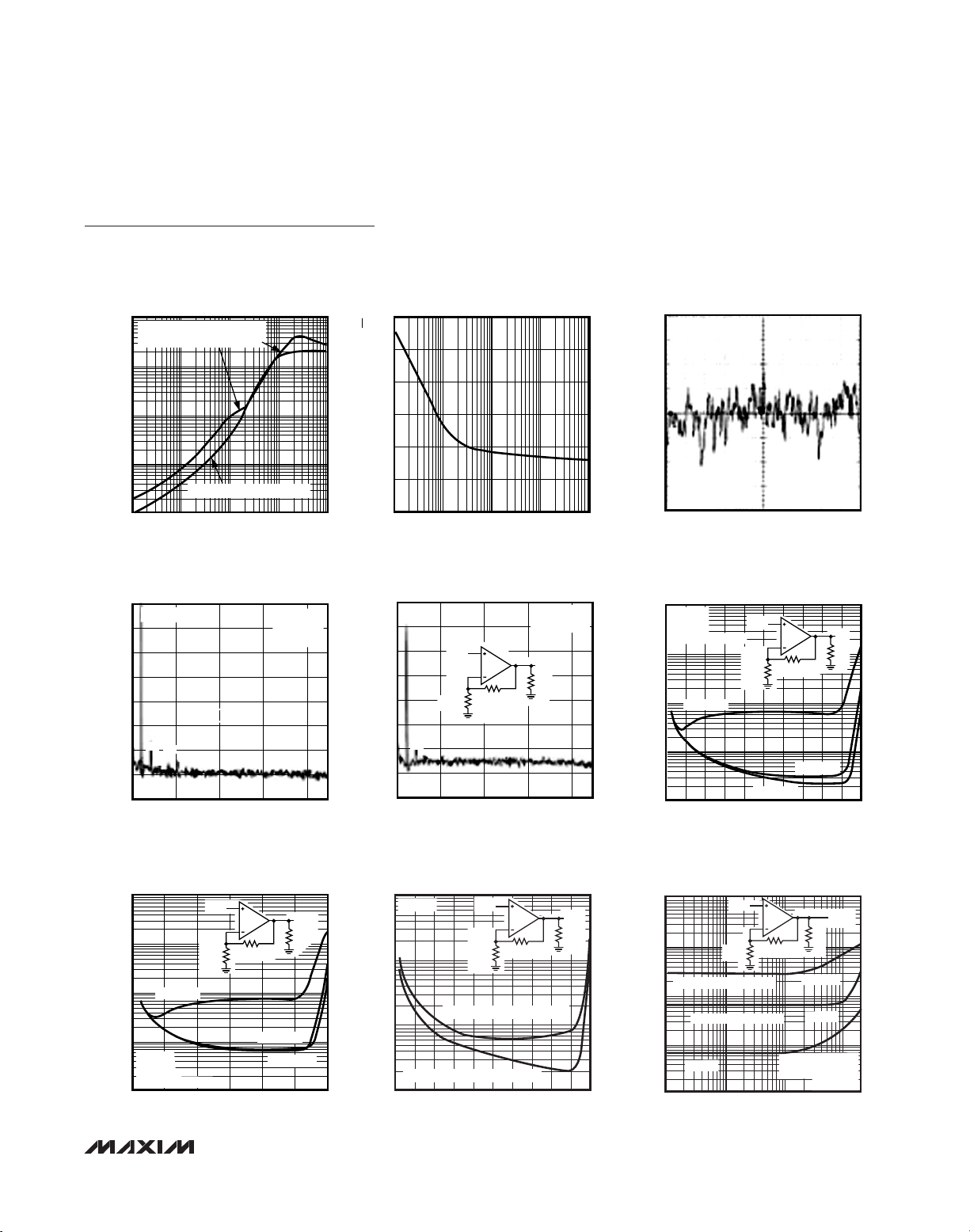
Page 7
MAX4249–MAX4257
UCSP, Single-Supply, Low-Noise,
Low-Distortion, Rail-to-Rail Op Amps
_______________________________________________________________________________________
7
1000
0.1
1k 10k 100k 1M 10M
OUTPUT IMPEDANCE
vs. FREQUENCY
MAX4249-57 TOC19
FREQUENCY (Hz)
OUTPUT IMPEDANCE (Ω)
1
10
100
A
V
= 1 (MAX4250–MAX4254)
AV = 10 (MAX4249/MAX4255/
MAX4256/MAX4257)
30
0
10 100 1k 10k 100k
INPUT VOLTAGE-N0ISE DENSITY
vs. FREQUENCY
MAX4249-57 TOC20
FREQUENCY (Hz)
Vn-EQUIVALENT INPUT NOISE-VOLTAGE (nV/√Hz)
5
10
15
20
25
200nV/div
1s/div
0.1Hz TO 10Hz
P-P
NOISE
MAX4249-57 TOC21
V
DD
= 3V OR 5V
V
P-PNOISE
= 760nV
P-P
-160
-140
-120
-100
-80
-60
-40
-20
0
MAX4250–MAX4254
FFT OF DISTORTION AND NOISE
FREQUENCY (Hz)
AMPLITUDE (dBc)
10 5k 10k
15k
20k
MAX4249-57 TOC22
RL = 1kΩ
f
O
= 1kHz
A
V
= 1
f
O
HD2
HD3
HD4
HD5
V
OUT
= 2V
P-P
-140
-120
-100
-80
-60
-40
-20
0
20
10 5k 10k
15k
20k
MAX4249/MAX4255/MAX4256/MAX4257
FFT OF DISTORTION AND NOISE
MAX4249-57 TOC23
FREQUENCY (Hz)
AMPLITUDE (dBc)
V
OUT
= 4V
P-P
fO = 1kHz
HD2
HD3
V
IN
10kΩ
100kΩ
11kΩ
f
O
V
O
0.001
0.01
0.1
1
10
021 345
MAX4250–MAX4254
TOTAL HARMONIC DISTORTION PLUS NOISE
vs. OUTPUT VOLTAGE (V
DD
= 5V)
MAX4249-57 TOC24
OUTPUT VOLTAGE (V
P-P
)
THD+N (%)
V
IN
RL = 1kΩ
100kΩ
11kΩ
AV = 10
f
O
= 3kHz
FILTER BW = 30kHz
V
O
R
L
RL = 10kΩ
R
L
= 100kΩ
0.001
0.01
0.1
1
10
0213
MAX4249-57 TOC25
OUTPUT VOLTAGE (V
P-P
)
THD+N (%)
100kΩ
11kΩ
MAX4250–MAX4254
TOTAL HARMONIC DISTORTION PLUS NOISE
vs. OUTPUT VOLTAGE SWING (V
DD
= 3V)
V
OUT
V
IN
R
L
RL = 1kΩ
R
L
= 10kΩ
R
L
= 100kΩ
A
V
= 10
f
O
= 3kHz
FILTER BW = 30kHz
Typical Operating Characteristics (continued)
(VDD= 5V, VSS= 0V, VCM= V
OUT
= VDD/2, input noise floor of test equipment =10nV/√Hz for all distortion measurements,
T
A
= +25°C, unless otherwise noted.)
MAX4249/MAX4255/MAX4256/MAX4257
TOTAL HARMONIC DISTORTION PLUS NOISE
vs. OUTPUT VOLTAGE SWING
1
A
= 10
V
0.1
THD+N (%)
0.01
fO = 3kHz, FILTER BW = 30kHz
0.001
03412 5
V
IN
100kΩ
11kΩ
fO = 20kHz, FILTER BW = 80kHz
OUTPUT VOLTAGE (V
)
P-P
V
R
OUT
L
MAX4249-57 TOC26
0.0001
MAX4250–MAX4254
TOTAL HARMONIC DISTORTION
PLUS NOISE vs. FREQUENCY
1
0.1
R1 = 560Ω, R2 = 53kΩ
0.01
THD+N (%)
0.001
10 1k100 10k
V
IN
R1
R1 = 5.6kΩ, R2 = 53kΩ
A
= 1
V
FREQUENCY (Hz)
R2
FILTER BW = 22kHz
R
V
OUT
R
L
A
= 100
V
A
= 10
V
= 10kΩ TO GND
L
V
= 2V
O
MAX4249-57 TOC27
P-P
Page 8

MAX4249–MAX4257
UCSP, Single-Supply, Low-Noise,
Low-Distortion, Rail-to-Rail Op Amps
8 _______________________________________________________________________________________
V
OUT
200mV/div
1.5V
0.5V
2µs/div
MAX4250–MAX4254
LARGE-SIGNAL PULSE RESPONSE
MAX4249-57 TOC29
VDD = 3V
R
L
= 10kΩ
C
L
= 100pF
V
IN
= 1V PULSE
0.6V
0.5V
MAX4249-57 TOC30
MAX4250–MAX4254
SMALL-SIGNAL PULSE RESPONSE
V
OUT
20mV/div
V
DD
= 3V
R
L
= 10kΩ
C
L
= 100pF
V
IN
= 100V PULSE
2µs/div
2V
1V
MAX4249/MAX4255/MAX4256/MAX4257
LARGE-SIGNAL PULSE RESPONSE
MAX4249-57 TOC31
V
OUT
200mV/div
V
DD
= 3V
R
L
= 10kΩ
C
L
= 100pF
V
IN
= 100mV PULSE
A
V
= 10
2µs/div
1.6V
1.5V
MAX4249/MAX4255/MAX4256/MAX4257
SMALL-SIGNAL PULSE RESPONSE
MAX4249-57 TOC32
V
OUT
50mV/div
V
DD
= 3V
R
L
= 10kΩ
C
L
= 100pF
V
IN
= 10mV PULSE
A
V
= 10
2µs/div
140
130
0
CHANNEL SEPARATION vs. FREQUENCY
MAX4249-57 TOC33
FREQUENCY (Hz)
CHANNEL SEPARATION (dB)
100
110
120
90
80
70
1k 100k 1M10k 10M
Typical Operating Characteristics (continued)
(VDD= 5V, VSS= 0V, VCM= V
OUT
= VDD/2, input noise floor of test equipment =10nV/√Hz for all distortion measurements,
T
A
= +25°C, unless otherwise noted.)
MAX4250–MAX4254
TOTAL HARMONIC DISTORTION
PLUS NOISE vs. FREQUENCY
0.1
FILTER BW = 80kHz
A
= 1
V
R
= 1kΩ
L
= 2V
V
OUT
0.01
THD+N(%)
0.001
0.0001
10 1k100 10k
P-P
RL TO VDD/2
FREQUENCY (Hz)
R
L
R
L
MAX4249-57 TOC28
TO GND
TO V
DD
Page 9

MAX4249–MAX4257
Detailed Description
The MAX4249–MAX4257 single-supply operational
amplifiers feature ultra-low noise and distortion while
consuming very little power. Their low distortion and low
noise make them ideal for use as preamplifiers in wide
dynamic-range applications, such as 16-bit analog-todigital converters (see
Typical Operating Circuit
). Their
high-input impedance and low noise are also useful for
signal conditioning of high-impedance sources, such
as piezoelectric transducers.
These devices have true rail-to-rail output operation,
drive loads as low as 1kΩ while maintaining DC accura-
cy, and can drive capacitive loads up to 400pF without
oscillation. The input common-mode voltage range
extends from VDD- 1.1V to 200mV beyond the negative
rail. The push-pull output stage maintains excellent DC
characteristics, while delivering up to ±5mA of current.
The MAX4250–4254 are unity-gain stable, whereas, the
MAX4249/MAX4255/MAX4256/MAX4257 have a higher
slew rate and are stable for gains ≥ 10V/V. The
MAX4249/MAX4251/MAX4253/MAX4256 feature a lowpower shutdown mode, which reduces the supply current to 0.5µA and disables the outputs.
The MAX4250AAUK is specified for operation over the
automotive (-40°C to +125°C) temperature range.
Pin/Bump Description
UCSP, Single-Supply, Low-Noise,
Low-Distortion, Rail-to-Rail Op Amps
_______________________________________________________________________________________
9
PIN/BUMP
M A X4 2 5 0 /
M A X4 2 5 5
5-PIN
SOT23
1 6 1, 7 A1, A3 A1, C1 1, 9 1, 13
244C2B44411
3 3 3, 5 C1, C3 A3, C3 3, 7 3, 11
4 2 2, 6 B1, B3 A2, C2 2, 8 2, 12
578A2B110144
— 8 — — A4, C4 5, 6 6, 9 —
— 1, 5 — — — —
— — — B2 B2, B3 — — — —
M A X4 2 5 1 /
M A X4 2 5 6
8-PIN
SO/µMAX
M A X4 2 5 2 /
M A X4 2 5 7
8-PIN
SO/µMAX
M A X4 2 5 2
8-BUMP
UCSP
10-BUMP
UCSP
M A X4 2 4 9 /
M A X4 2 5 3
10-PIN
µMAX
M A X4 2 5 4
1 4 - PINSO14-PIN
5, 7,
8, 10
SO
1, 7, 8,
14
3, 5, 10,
12
2, 6, 9,
13
—N.C.
NAME FUNCTION
OUT, OUTA,
OUTB,
OUTC,
OUTD
V
SS
IN + , IN A+ ,
IN B+ , IN C + ,
IN D +
IN-, INA-,
INB-,
INC-, IND-
V
DD
SHDN,
SHDNA,
SHDNB
Amplifier Output
Negative Supply.
Connect to
ground for singlesupply operation
Noninverting
Amplifier Input
Inverting
Amplifier Input
Positive Supply
Shutdown Input,
Connect to V
or leave
unconnected for
normal operation
(amplifier(s)
enabled).
No Connection.
Not internally
connected.
Not populated
with solder
sphere
DD
Page 10

MAX4249–MAX4257
UCSP, Single-Supply, Low-Noise,
Low-Distortion, Rail-to-Rail Op Amps
10 ______________________________________________________________________________________
Low Distortion
Many factors can affect the noise and distortion that the
device contributes to the input signal. The following
guidelines offer valuable information on the impact of
design choices on Total Harmonic Distortion (THD).
Choosing proper feedback and gain resistor values for
a particular application can be a very important factor
in reducing THD. In general, the smaller the closedloop gain, the smaller the THD generated, especially
when driving heavy resistive loads. Large-value feedback resistors can significantly improve distortion. The
THD of the part normally increases at approximately
20dB per decade, as a function of frequency.
Operating the device near or above the full-power
bandwidth significantly degrades distortion.
Referencing the load to either supply also improves the
part’s distortion performance, because only one of the
MOSFETs of the push-pull output stage drives the output. Referencing the load to midsupply increases the
part’s distortion for a given load and feedback setting.
(See the Total Harmonic Distortion vs. Frequency graph
in the
Typical Operating Characteristics
.)
For gains ≥ 10V/V, the decompensated devices
MAX4249/MAX4255/MAX4256/MAX4257 deliver the
best distortion performance, since they have a higher
slew rate and provide a higher amount of loop gain for
a given closed-loop gain setting. Capacitive loads
below 400pF, do not significantly affect distortion
results. Distortion performance remains relatively constant over supply voltages.
Low Noise
The amplifier’s input-referred, noise-voltage density is
dominated by flicker noise at lower frequencies, and by
thermal noise at higher frequencies. Because the thermal noise contribution is affected by the parallel combination of the feedback resistive network (R
F
|| RG,
Figure 1), these resistors should be reduced in cases
where the system bandwidth is large and thermal noise
is dominant. This noise contribution factor decreases,
however, with increasing gain settings.
For example, the input noise-voltage density of the circuit with R
F
= 100kΩ, RG= 11kΩ (AV= 10V/V) is en=
15nV/√Hz, encan be reduced to 9nV/√Hz by choosing
R
F
= 10kΩ, RG= 1.1kΩ (AV= 10V/V), at the expense
of greater current consumption and potentially higher
distortion. For a gain of 100V/V with R
F
= 100kΩ, RG=
1.1kΩ, the enis low (9nV/√Hz).
Figure 1. Adding Feed-Forward Compensation
Figure 2a. Pulse Response with No Feed-Forward
Compensation
Figure 2b. Pulse Response with 10pF Feed-Forward
Compensation
R
100mV
100mV
V
V
G
0
IN
0
OUT
V
AV = 2V/V
= RG = 10kΩ
R
F
AV = 2
= RG = 100kΩ
R
F
= 11pF
C
Z
C
Z
R
F
V
OUT
IN
VIN =
50mV/div
V
=
OUT
100mV/div
2µs/div
50mV/div
100mV/div
2µs/div
Page 11

MAX4249–MAX4257
UCSP, Single-Supply, Low-Noise,
Low-Distortion, Rail-to-Rail Op Amps
______________________________________________________________________________________ 11
Using a Feed-Forward Compensation
Capacitor, C
Z
The amplifier’s input capacitance is 11pF. If the resistance seen by the inverting input is large (feedback
network), this can introduce a pole within the amplifier’s
bandwidth, resulting in reduced phase margin.
Compensate the reduced phase margin by introducing
a feed-forward capacitor (CZ) between the inverting
input and the output (Figure 1). This effectively cancels
the pole from the inverting input of the amplifier.
Choose the value of CZas follows:
C
Z
= 11 x (RF/ RG) [pF]
In the unity-gain stable MAX4250–MAX4254, the use of
a proper C
Z
is most important for AV= 2V/V, and
AV = -1V/V. In the decompensated MAX4249/
MAX4255/MAX4256/MAX4257, CZis most important
for AV= 10V/V. Figures 2a and 2b show transient
response both with and without CZ.
Using a slightly smaller CZthan suggested by the formula above achieves a higher bandwidth at the
expense of reduced phase and gain margin. As a general guideline, consider using CZfor cases where RG||
RFis greater than 20kΩ (MAX4250–MAX4254) or
greater than 5kΩ (MAX4249/MAX4255/MAX4256/
MAX4257).
Applications Information
The MAX4249–MAX4257 combine good driving capability with ground-sensing input and rail-to-rail output
operation. With their low distortion, low noise, and lowpower consumption, these devices are ideal for use in
portable instrumentation systems and other low-power,
noise-sensitive applications.
Ground-Sensing and Rail-to-Rail Outputs
The common-mode input range of these devices
extends below ground, and offers excellent commonmode rejection. These devices are guaranteed not to
undergo phase reversal when the input is overdriven
(Figure 3).
Figure 4 showcases the true rail-to-rail output operation
of the amplifier, configured with AV= 10V/V. The output
swings to within 8mV of the supplies with a 10kΩ load,
making the devices ideal in low-supply-voltage applications.
Output Loading and Stability
Even with their low quiescent current of 400µA, these
amplifiers can drive 1kΩ loads while maintaining excellent DC accuracy. Stability while driving heavy capacitive loads is another key feature.
Figure 3. Overdriven Input Showing No Phase Reversal
Figure 4. Rail-to-Rail Output Operation
Figure 5. Capacitive-Load Driving Circuit
R
ISO
C
V
IN
4.25V
0
4.45V
0
MAX4250
MAX4251
MAX4252
MAX4253
MAX4254
AV = 1
VDD = 5V
RL = 10kΩ
20µs/div
L
V
OUT
V
IN
-200mV
V
OUT
5V
0
VDD = 5V
RL = 10kΩ
= 10
A
V
f = 1kHz
200µs/div
V
OUT
1V/div
Page 12

UCSP, Single-Supply, Low-Noise,
Low-Distortion, Rail-to-Rail Op Amps
12 ______________________________________________________________________________________
These devices maintain stability while driving loads up
to 400pF. To drive higher capacitive loads, place a
small isolation resistor in series between the output of
the amplifier and the capacitive load (Figure 5). This
resistor improves the amplifier’s phase margin by isolating the capacitor from the op amp’s output. Reference
Figure 6 to select a resistance value that will ensure a
load capacitance that limits peaking to <2dB (25%).
For example, if the capacitive load is 1000pF, the corresponding isolation resistor is 150Ω. Figure 7 shows that
peaking occurs without the isolation resistor. Figure 8
shows the unity-gain bandwidth vs. capacitive load for
the MAX4250–MAX4254.
Power Supplies and Layout
The MAX4249–MAX4257 operate from a single 2.4V to
5.5V power supply or from dual supplies of ±1.20V to
±2.75V. For single-supply operation, bypass the power
supply with a 0.1µF ceramic capacitor placed close to
the V
DD
pin. If operating from dual supplies, bypass
each supply to ground.
Good layout improves performance by decreasing the
amount of stray capacitance and noise at the op amp’s
inputs and output. To decrease stray capacitance, minimize PC board trace lengths and resistor leads, and
place external components close to the op amp’s pins.
UCSP Applications Information
For the latest application details on UCSP construction,
dimensions, tape carrier information, PC board techniques, bump-pad layout, and recommended reflow
temperature profile, as well as the latest information on
reliability testing results, refer to the Application Note:
UCSP—A Wafer-Level Chip-Scale Package
on Maxim’s
web site at www.maxim-ic.com/ucsp
.
Figure 6. Isolation Resistance vs. Capacitive Loading to
Minimize Peaking (<2dB)
Figure 7. Peaking vs. Capacitive Load
Figure 8. MAX4250–MAX4254 Unity-Gain Bandwidth vs.
Capacitive Load
160
140
120
100
(Ω)
80
ISO
R
60
40
20
0
10 10,000
NOTE: USING AN ISOLATION RESISTOR REDUCES PEAKING.
SHADED AREA INDICATES
STABLE OPERATION
WITH NO NEED FOR
ISOLATION RESISTOR.
CAPACITIVE LOADING (pF)
1000100
25
MAX4250–MAX4254 (A
MAX4249/MAX4255–MAX4257 (A
R
= 0
ISO
20
SHADED AREA INDICATES
15
STABLE OPERATION
WITH NO NEED FOR
ISOLATION RESISTOR.
10
PEAKING (dB)
5
0
10 10,000
= 1)
V
CAPACITIVE LOAD (pF)
1000100
= 10)
V
4.5
4.0
3.5
3.0
2.5
2.0
1.5
SHADED AREA INDICATES
1.0
UNITY-GAIN BANDWIDTH (MHz)
STABLE OPERATION
WITH NO NEED FOR
0.5
ISOLATION RESISTOR.
0
10 10,000
CAPACITIVE LOAD (pF)
CHOSEN FOR PEAKING <2dB.
NOTE: R
ISO
V
= 3V
DD
1000100
Page 13

MAX4249–MAX4257
UCSP, Single-Supply, Low-Noise,
Low-Distortion, Rail-to-Rail Op Amps
______________________________________________________________________________________ 13
Typical Operating Circuit
Selector Guide
5V
V
50kΩ
2
V
IN
3
5kΩ
MAX4256
4
7
6
8
AIN
SHDN
DD
MAX195
(16-BIT ADC)
V
SS
-5V
DOUT
SCLK
CS
REF
SERIAL
INTERFACE
4.096V
SHDN
G A IN
PART
MAX4249 22 10 2 Yes 10-pin µMAX, 14-pin SO
MAX4250/A 3 1 1 — 5-pin SOT23
MAX4251 3 1 1 Yes 8-pin µMAX/SO
MAX4252 3 1 2 — 8- p i n µM AX /S O , 8- b um p U C S P
MAX4253 3 1 2 Yes
MAX4254 3 1 4 — 14-pin SO
MAX4255 22 10 1 — 5-pin SOT23
MAX4256 22 10 1 Yes 8-pin µMAX/SO
MAX4257 22 10 2 — 8-pin µMAX/SO
B A N D WID T H
( M H z)
MINIMUM
STABLE
GAIN (V/V)
NO. OF
AMPLIFIERS
PER PACKAGE
SHUTDOWN
MODE
PIN-PACKAGE
10-pin µMAX, 14-pin SO,
10-bump UCSP
Page 14

Pin/Bump Configurations (continued)
MAX4249–MAX4257
UCSP, Single-Supply, Low-Noise,
Low-Distortion, Rail-to-Rail Op Amps
14 ______________________________________________________________________________________
Ordering Information (continued)
TOP VIEW
OUT
V
SS
MAX4250A
MAX4250
2
DD
+
15V
MAX4255
34
IN-IN+
SOT23
+
OUTA
1
INA-
2
INA+
SS
MAX4249
3
MAX4253
4
5
μMAX
10
V
DD
9
OUTB
8
INB-
7
INB+V
SHDNBSHDNA
6
SHDNA
N.C.
IN-
IN+
SS
OUTA
INA-
INA+
N.C.
+
1
2
MAX4251
MAX4256
3
4
87SHDN
V
DD
OUT
6
N.C.V
5
OUTA
INA+
μMAX/SO
+
1
2
3
4
5
6
7
MAX4249
MAX4253
SS
V
14
DD
13
OUTB
12
INB-
11
INB+V
10
N.C.
9
SHDNB
8
N.C.N.C.
OUTA
INA-
INA+
V
INB+
INB-
SO
+
1
2
87V
DD
OUTBINA-
MAX4252
MAX4257
3
4
SS
INB-
6
INB+V
5
μMAX/SO
+
1
2
3
4
DD
MAX4254
5
6
7
OUTD
14
IND-
13
IND+
12
V
11
SS
10
INC+
9
INC-
8
OUTCOUTB
SO
PART TEMP RANGE
MAX4251ESA+
-40°C to +85°C 8 SO —
PINPACKAGE
MAX4251EUA+ -40°C to +85°C 8 µMAX —
MAX4252EBL+T
-40°C to +85°C 8 UCSP AAO
MAX4252ESA+ -40°C to +85°C 8 SO —
MAX4252EUA+ -40°C to +85°C 8 µMAX —
MAX4253EBC+T
-40°C to +85°C 10 UCSP AAK
MAX4253EUB+ -40°C to +85°C 10 µMAX —
MAX4253ESD+ -40°C to +85°C 14 SO —
MAX4254ESD+
MAX4255EUK+T
MAX4256ESA+
-40°C to +85°C 14 SO —
-40°C to +85°C 5 SOT23 AC C J
-40°C to +85°C 8 SO —
MAX4256EUA+ -40°C to +85°C 8 µMAX —
MAX4257ESA+
-40°C to +85°C 8 SO —
MAX4257EUA+ -40°C to +85°C 8 µMAX —
TOP
M ARK
Page 15

MAX4249–MAX4257
UCSP, Single-Supply, Low-Noise,
Low-Distortion, Rail-to-Rail Op Amps
______________________________________________________________________________________ 15
Package Information
For the latest package outline information and land patterns (footprints), go to www.maxim-ic.com/packages. Note that a "+", "#", or
"-" in the package code indicates RoHS status only. Package drawings may show a different suffix character, but the drawing pertains to the package regardless of RoHS status.
PACKAGE TYPE PACKAGE CODE OUTLINE NO.
5 SOT-23 U5+2 21-0057 90-0174
8 µMAX U8+1 21-0036 90-0092
10 µMAX U10+2 21-0061 90-0330
3 x 3 µCSP B9+5 21-0093 —
14 SOIC S14+1 21-0041 90-0112
12 µCSP B12+4 21-0104 —
LAND
PATTERN NO.
Page 16

MAX4249–MAX4257
UCSP, Single-Supply, Low-Noise,
Low-Distortion, Rail-to-Rail Op Amps
16 ______________________________________________________________________________________
Package Information (continued)
For the latest package outline information and land patterns (footprints), go to www.maxim-ic.com/packages. Note that a "+", "#", or
"-" in the package code indicates RoHS status only. Package drawings may show a different suffix character, but the drawing pertains to the package regardless of RoHS status.
α
α
Page 17

MAX4249–MAX4257
UCSP, Single-Supply, Low-Noise,
Low-Distortion, Rail-to-Rail Op Amps
______________________________________________________________________________________ 17
Package Information (continued)
For the latest package outline information and land patterns (footprints), go to www.maxim-ic.com/packages. Note that a "+", "#", or
"-" in the package code indicates RoHS status only. Package drawings may show a different suffix character, but the drawing pertains to the package regardless of RoHS status.
α
α
Page 18

MAX4249–MAX4257
UCSP, Single-Supply, Low-Noise,
Low-Distortion, Rail-to-Rail Op Amps
18 ______________________________________________________________________________________
Package Information (continued)
For the latest package outline information and land patterns (footprints), go to www.maxim-ic.com/packages. Note that a "+", "#", or
"-" in the package code indicates RoHS status only. Package drawings may show a different suffix character, but the drawing pertains to the package regardless of RoHS status.
9LUCSP, 3x3.EPS
Page 19

MAX4249–MAX4257
UCSP, Single-Supply, Low-Noise,
Low-Distortion, Rail-to-Rail Op Amps
______________________________________________________________________________________ 19
Package Information (continued)
For the latest package outline information and land patterns (footprints), go to www.maxim-ic.com/packages. Note that a "+", "#", or
"-" in the package code indicates RoHS status only. Package drawings may show a different suffix character, but the drawing pertains to the package regardless of RoHS status.
Page 20

MAX4249–MAX4257
UCSP, Single-Supply, Low-Noise,
Low-Distortion, Rail-to-Rail Op Amps
20 ______________________________________________________________________________________
Package Information (continued)
For the latest package outline information and land patterns (footprints), go to www.maxim-ic.com/packages. Note that a "+", "#", or
"-" in the package code indicates RoHS status only. Package drawings may show a different suffix character, but the drawing pertains to the package regardless of RoHS status.
Page 21

UCSP, Single-Supply, Low-Noise,
Low-Distortion, Rail-to-Rail Op Amps
REVISION
NUMBER
8 10/11
REVISION
DATE
Revision History
DESCRIPTION
Added lead-free packaging to the Ordering Information and changed the Input Bias
Current and Input Offset Current conditions in the Electrical Characteristics table
MAX4249–MAX4257
PAGES
CHANGED
1, 2, 14
Maxim cannot assume responsibility for use of any circuitry other than circuitry entirely embodied in a Maxim product. No circuit patent licenses are
implied. Maxim reserves the right to change the circuitry and specifications without notice at any time. The parametric values (min and max limits) shown in
the Electrical Characteristics table are guaranteed. Other parametric values quoted in this data sheet are provided for guidance.
21
____________________Maxim Integrated Products, 120 San Gabriel Drive, Sunnyvale, CA 94086 408-737-7600
© 2011 Maxim Integrated Products Maxim is a registered trademark of Maxim Integrated Products, Inc.
 Loading...