

General Description
The MAX4236/MAX4237 are high-precision op amps
that feature an exceptionally low offset voltage and offset voltage temperature coefficient without using any
chopper techniques. The MAX4236 and MAX4237 have
a typical large-signal, open-loop voltage gain of 120dB.
These devices have an ultra-low input-bias current of
1pA. The MAX4236 is unity-gain stable with a gainbandwidth product of 1.7MHz, while the MAX4237 is
stable for closed-loop gains greater than 5V/V with a
gain-bandwidth product of 7.5MHz. Both devices have
a shutdown function in which the quiescent current is
reduced to less than 0.1µA, and the amplifier output is
forced into a high-impedance state.
The input common-mode range of the MAX4236/
MAX4237 extends below the negative supply range, and
the output swings Rail-to-Rail®. These features make the
amplifiers ideal for applications with +3V or +5V single
power supplies. The MAX4236/MAX4237 are specified for
the extended temperature range (-40°C to +85°C) and
are available in tiny SOT23, µMAX, and SO packages. For
greater accuracy, the A grade µMAX and SO packages
are tested to guarantee 20µV (max) offset voltage at
+25°C and less then 2µV/°C drift.
Applications
Strain Gauges
Piezoelectric Sensors
Thermocouple Amplifiers
Electrochemical Sensors
Battery-Powered Instrumentation
Instrumentation Amplifiers
Features
♦ Ultra-Low Offset Voltage
20µV (max) at +25°C (Grade A)
50µV (max) at +25°C (Grade B, 6-Pin SOT23)
♦ Ultra-Low Offset Voltage Drift
2µV/°C (max) (Grade A)
4.5µV/°C (max) (Grade B, 6-Pin SOT23)
5.5µV/°C (max) (6-Pin SOT23)
♦ Ultra-Low 1pA Input Bias Current
♦ High Open-Loop Voltage Gain: 110dB (min)
(R
L
= 100kΩ)
♦ Compatible with +3V and +5V Single-Supply
Power Systems
♦ Ground Sensing: Input Common-Mode Range
Includes Negative Rail
♦ Rail-to-Rail Output Swing into a 1kΩ Load
♦ 350µA Quiescent Current
♦ Gain-Bandwidth Product
1.7MHz (MAX4236, A
V
= 1V/V)
7.5MHz (MAX4237, A
V
= 5V/V)
♦ 200pF Capacitive Load Handling Capability
♦ Shutdown Mode: 0.1µA Quiescent Current,
Places Output in a High-Impedance State
♦ Available in Space-Saving SOT23 and µMAX
Packages
MAX4236/MAX4237
SOT23, Very High Precision, 3V/5V
Rail-to-Rail Op Amps
________________________________________________________________ Maxim Integrated Products 1
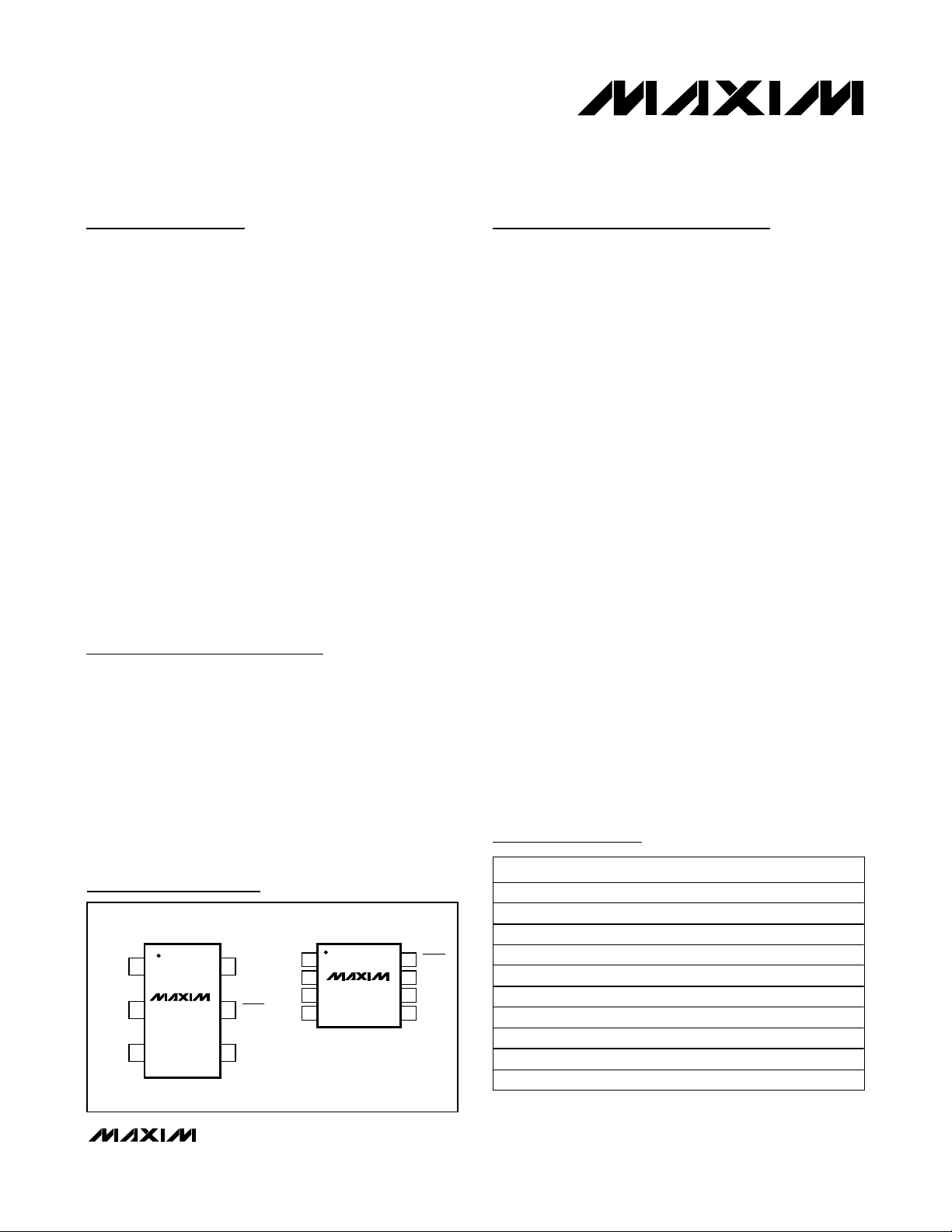
Pin Configurations
Ordering Information
19-2110; Rev 0; 8/01
For pricing, delivery, and ordering information, please contact Maxim/Dallas Direct! at
1-888-629-4642, or visit Maxim’s website at www.maxim-ic.com.
Rail-to-Rail is a registered trademark of Nippon Motorola, Inc.
TOP VIEW
OUT
16V
V
MAX4236
2
EE
MAX4237
34
SOT23-6
CC
5 SHDN
IN-IN+
N.C.
IN-
IN+
EE
1
2
MAX4236A/B
3
MAX4237A/B
4
SO-8/µMAX
8
SHDN
7
V
CC
6
OUT
5
N.C.V
PART TEMP. RANGE PIN-PACKAGE
MAX4236EUT-T -40°C to +85°C 6 SOT23-6
MAX4236AEUA -40°C to +85°C 8 µMAX
MAX4236BEUA -40°C to +85°C 8 µMAX
MAX4236AESA -40°C to +85°C 8 SO
MAX4236BESA -40°C to +85°C 8 SO
MAX4237EUT-T -40°C to +85°C 6 SOT23-6
MAX4237AEUA -40°C to +85°C 8 µMAX
MAX4237BEUA -40°C to +85°C 8 µMAX
MAX4237AESA -40°C to +85°C 8 SO
MAX4237BESA -40°C to +85°C 8 SO

MAX4236/MAX4237
SOT23, Very High Precision, 3V/5V
Rail-To-Rail Op Amps
2 _______________________________________________________________________________________
ABSOLUTE MAXIMUM RATINGS
ELECTRICAL CHARACTERISTICS (SO-8 and µMAX-8)
(VCC= +2.4V to +5.5V, VEE= 0, VCM= 0, V
OUT
= VCC/2, RL= 100kΩ to VCC/2, TA= T
MIN
to T
MAX
, unless otherwise noted. Typical
values are at V
CC
= +5V and TA= +25°C.) (Note 1)
Stresses beyond those listed under “Absolute Maximum Ratings” may cause permanent damage to the device. These are stress ratings only, and functional
operation of the device at these or any other conditions beyond those indicated in the operational sections of the specifications is not implied. Exposure to
absolute maximum rating conditions for extended periods may affect device reliability.
Supply Voltage (VCC- VEE)......................................-0.3V to +6V
Analog Input Voltage (IN+ or IN-)....(V
EE
- 0.3V) to (VCC+ 0.3V)
Logic Input Voltage (SHDN) ............(V
EE
- 0.3V) to (VCC+ 0.3V)
Current into Any Pin ............................................................20mA
Output Short-Circuit Duration....Continuous to Either V
CC
or V
EE
Continuous Power Dissipation (TA= +70°C)
6-Pin SOT23-6 (derate 8.7mW/°C above +70°C) .........696mW
8-Pin µMAX (derate 4.5mW/°C above +70°C) ..............362mW
8-Pin SO (derate 5.9mW/°C above +70°C)...................471mW
Operating Temperature Range ...........................-40°C to +85°C
Junction Temperature......................................................+150°C
Storage Temperature Range .............................-65°C to +150°C
Lead Temperature (soldering, 10s) .................................+300°C
PARAMETER SYMBOL CONDITIONS MIN TYP MAX UNITS
Supply Voltage Range V
Quiescent Supply Current I
Input Offset Voltage V
Inp ut Offset V ol tag e Tem p er atur e
C oeffi ci ent
CC
CC
OS
TCV
Input Bias Current I
Input Offset Current I
OS
Input Resistance R
Guaranteed by the PSRR test 2.4 5.5 V
VCC = +5V
VCC = +3V
VCC = +5V,
Grade A
VCC = +5V,
Grade B
VCC = +5V
OS
(Note 3)
B
(Note 2) ±1 ±500 pA
(Note 2) ±1 pA
Differential or common mode 1000 MΩ
IN
In normal mode 350 440
In shutdown mode 0.1 2
In normal mode 350 440
In shutdown mode 0.1 2
TA = +25oC ±5 ±20
T
= T
MIN
to T
MAX
A
±150
TA = +25oC ±5 ±50
T
= T
MIN
to T
MAX
A
±340
Grade A ±0.6 ±2
Grade B ±0.6 ±4.5
µA
µV
µV/°C
Input Common-Mode Voltage V
CM
Common-Mode Rejection Ratio CMRR
Power-Supply Rejection Ratio PSRR
Guaranteed by the CMRR test -0.15 V
VCC = +5V;
-0.15V ≤ V
- 1.2V)
(V
CC
V
= +3.0V;
CC
-0.15V ≤ V
- 1.2V)
(V
CC
V
= +2.4V to
CC
+5.5V
CM
CM
≤
≤
TA = +25oC 84 102
T
= T
MIN
to T
MAX
A
80
TA = +25oC 82 102
TA = T
MIN
to T
MAX
78
TA = +25oC 97 120
T
= T
MIN
to T
MAX
A
95
- 1.2 V
C C
dB
dB
MAX4236/MAX4237
SOT23, Very High Precision, 3V/5V
Rail-To-Rail Op Amps
_______________________________________________________________________________________ 3
ELECTRICAL CHARACTERISTICS (SO-8 and µMAX-8) (continued)
(VCC= +2.4V to +5.5V, VEE= 0, VCM= 0, V
OUT
= VCC/2, RL= 100kΩ to VCC/2, TA= T
MIN
to T
MAX
, unless otherwise noted. Typical
values are at V
CC
= +5V and TA= +25°C.) (Note 1)
)
PARAMETER SYMBOL CONDITIONS MIN TYP MAX UNITS
Large-Signal Voltage Gain A
VOL
RL = 100kΩ, V
VCC = +5V, R
L
15mV to (V
connected to
/2,
V
CC
T
= +25oC
A
VCC = +5V, R
connected to
V
/2,
CC
= T
MIN
to
T
T
A
MAX
L
RL = 1kΩ, V
0.15V to (V
RL = 100kΩ, V
15mV to (V
RL = 1kΩ,
= 0.15V
V
OUT
to (V
CC
RL = 100kΩ, V
VCC = +3V, R
connected to
/2,
V
CC
T
= +25oC
A
VCC = +3V, R
connected to
V
/2,
CC
= T
T
A
T
MAX
MIN
to
L
L
15mV to (V
R
= 1kΩ,
L
V
= 0.15V
OUT
to (V
CC
RL = 100kΩ, V
15mV to (V
RL = 1kΩ,
= 0.15V
V
OUT
to (V
CC
CC
OUT
CC
CC
- 0.3V)
CC
- 0.3V)
CC
- 0.3V)
=
OUT
- 50mV)
=
- 0.3V)
=
OUT
- 50mV)
=
OUT
- 50mV)
=
OUT
- 50mV)
110 128
105 114
110
100
dB
110 128
100 114
105
95
VCC = +5V,
R
connected to V
L
= 100kΩ
R
L
Output Voltage Swing V
OUT
VCC = +5V,
connected to VCC/2,
R
L
R
= 1kΩ
L
Output Short-Circuit Current I
OUT(SC
Shorted to V
Shorted to V
EE
CC
Gain-Bandwidth Product GBWP RL = ∞, CL = 5pF
Slew Rate SR VCC = +5V, V
V
OUT
Settling Time t
S
Total Harmonic Distortion THD
0.01%
f = 5kHz, V
R
= 10kΩ
L
OUT
settling to within
OUT
VCC - V
/2,
CC
V
OL - VEE
VCC - V
V
OL - VEE
MAX4236 1.7
MAX4237 7.5
= 4V step
MAX4236 0.3
MAX4237 1.3
MAX4236 1
MAX4237 1
= 2Vp-p, VCC = +5V
OH
OH
210
310
mV
150 250
50 100
10
30
mA
MHz
V/µs
µs
0.001 %
MAX4236/MAX4237
SOT23, Very High Precision, 3V/5V
Rail-To-Rail Op Amps
4 _______________________________________________________________________________________
ELECTRICAL CHARACTERISTICS (SO-8 and µMAX-8) (continued)
(VCC= +2.4V to +5.5V, VEE= 0, VCM= 0, V
OUT
= VCC/2, RL= 100kΩ to VCC/2, TA= T
MIN
to T
MAX
, unless otherwise noted. Typical
values are at V
CC
= +5V and TA= +25°C.) (Note 1)
ELECTRICAL CHARACTERISTICS (SOT23-6)
(VCC= +2.4V to +5.5V, VEE= 0, VCM= 0, V
OUT
= VCC/2, RL= 100kΩ to VCC/2, TA= T
MIN
to T
MAX
, unless otherwise noted. Typical
values are at V
CC
= +5V and TA= +25°C.) (Note 1)
)
PARAMETER SYMBOL CONDITIONS MIN TYP MAX UNITS
Input Capacitance C
Input Voltage Noise Density e
Input Noise Voltage e
Capacitive Load Stability C
Shutdown Mode Output
Leakage
np-p
LOAD
I
OUT(SH
SHDN Logic Low V
SHDN Logic High V
SHDN Input Current SHDN = VEE or V
Shutdown Delay Time t
Shutdown Recovery Time t
(SH)
(EN)
f = 100kHz 7.5 pF
IN
f = 1kHz 14 nV/√Hz
n
f = 0.1Hz to 10Hz 0.2 µVp-p
No sustained oscillations
MAX4236 200
MAX4237 200
Device in shutdown mode (SHDN = VEE)
V
= 0 to V
OUT
IL
IH
CC
CC
RL = 1kΩ 1µs
RL = 1kΩ 4µs
±0.01 ±1.0 µA
✕
0.7
V
CC
13µA
0.3
V
CC
pF
✕
V
V
PARAMETER SYMBOL CONDITIONS MIN TYP MAX UNITS
Supply Voltage Range V
Quiescent Supply Current I
Input Offset Voltage V
Inp ut Offset V ol tag e Tem p er atur e
C oeffi ci ent ( N ote 2)
TCV
Input Bias Current I
Input Offset Current I
Input Resistance R
Input Common-Mode Voltage V
Common-Mode Rejection Ratio CMRR
Guaranteed by the PSRR test 2.4 5.5 V
CC
VCC = +5V
CC
VCC = +3V
VCC = +5V
OS
OSVCC
B
OS
IN
CM
= +5V ±0.6 ±5.5 µV/°C
(Note 2) ±1 ±500 pA
(Note 2) ±1 pA
Differential or common mode 1000 MΩ
Guaranteed by the CMRR test -0.15 V
VCC = +5V, -0.15V
≤ (VCC - 1.2V)
≤ V
CM
VCC = +3.0V; -0.15V
≤ (VCC - 1.2V)
≤ V
CM
In normal mode 350 440
In shutdown mode 0.1 2
In normal mode 350 440
In shutdown mode 0.1 2
TA = +25°C ±5 ±50
= T
MIN
to T
MAX
T
A
±600
- 1.2 V
C C
TA = +25°C 82 102
T
= T
MIN
to T
MAX
A
80
TA = +25°C 82 102
T
= T
MIN
to T
MAX
A
78
µA
µV
dB
MAX4236/MAX4237
SOT23, Very High Precision, 3V/5V
Rail-To-Rail Op Amps
_______________________________________________________________________________________ 5
ELECTRICAL CHARACTERISTICS (SOT23-6) (continued)
(VCC= +2.4V to +5.5V, VEE= 0, VCM= 0, V
OUT
= VCC/2, RL= 100kΩ to VCC/2, TA= T
MIN
to T
MAX
, unless otherwise noted. Typical
values are at V
CC
= +5V and TA= +25°C.) (Note 1)
)
PARAMETER SYMBOL CONDITIONS MIN TYP MAX UNITS
Power-Supply Rejection Ratio PSRR
Large-Signal Voltage Gain A
VOL
V
= +2.4V to
CC
+5.5V
TA = +25°C 97 120
T
= T
A
MIN
RL = 100kΩ,
= 15mV to
V
OUT
VCC = +5V, R
connected to
V
/2,
CC
= +25°C
T
A
VCC = +5V, R
connected to
V
/2,
CC
TA = T
T
MAX
MIN
to
L
L
(V
- 50mV)
CC
R
= 1kΩ,
L
= 0.15V
V
OUT
to (V
CC
RL = 100kΩ, V
15mV to (V
RL = 1kΩ,
V
= 0.15V to
OUT
- 0.3V)
(V
CC
RL = 100kΩ,
V
= 15mV to
VCC = +3V, R
connected to
/2,
V
CC
T
= +25°C
A
VCC = +3V, R
connected to
/2,
V
CC
T
= T
MIN
to
T
A
MAX
L
L
OUT
- 50mV)
(V
CC
R
= 1kΩ,
L
= 0.15V to
V
OUT
(V
- 0.3V)
CC
RL = 100kΩ,
V
= 15mV to
OUT
- 50mV)
(V
CC
RL = 1kΩ,
= 0.15V to
V
OUT
(V
- 0.3V)
CC
to T
- 0.3V)
CC
MAX
=
OUT
- 50mV)
95
110 128
100 114
110
95
110 128
100 114
105
95
dB
dB
VCC = +5V,
connected to VCC/2,
R
L
R
= 100kΩ
L
Output Voltage Swing V
OUT
VCC = +5V,
R
connected to VCC/2,
L
= 1kΩ
R
L
Shorted to V
Output Short-Circuit Current I
OUT(SC
Shorted to V
Gain-Bandwidth Product GBWP RL = ∞, CL = 15pF
V
Slew Rate SR
V
CC
OUT
= +5V,
= 4V step
EE
CC
VCC - V
- V
V
OL
VCC - V
V
- V
OL
OH
EE
OH
EE
210
310
150 250
50 100
10
30
MAX4236 1.7
MAX4237 7.5
MAX4236 0.3
MAX4237 1.3
mV
mA
MHz
V/µs
MAX4236/MAX4237
SOT23, Very High Precision, 3V/5V
Rail-To-Rail Op Amps
6 _______________________________________________________________________________________
Typical Operating Characteristics
(VCC= +5V, VEE= 0, VCM= VCC/2, RL= 100kΩ to VCC/2, TA= +25°C, unless otherwise noted.)
ELECTRICAL CHARACTERISTICS (SOT23-6) (continued)
(VCC= +2.4V to +5.5V, VEE= 0, VCM= 0, V
OUT
= VCC/2, RL= 100kΩ to VCC/2, TA= T
MIN
to T
MAX
, unless otherwise noted. Typical
values are at V
CC
= +5V and TA= +25°C.) (Note 1)
)
Note 1: All devices are 100% production tested at TA= +25°C; all specifications over temperature are guaranteed by design,
unless otherwise specified.
Note 2: Guaranteed by design, not production tested.
Note 3: Maxim specification limits for the temperature coefficient of the offset voltage (TCV
OS
) are 100% tested for the A-grade, 8-
pin SO and µMAX packages.
PARAMETER SYMBOL CONDITIONS MIN TYP MAX UNITS
Settling Time t
S
Total Harmonic Distortion THD
Input Capacitance C
Input Voltage Noise Density e
Input Noise Voltage e
Capacitive Load Stability C
IN
n
np-p
LOAD
V
settling to within 0.01%
OUT
f = 5kHz, V
R
= 10kΩ
L
OUT
= 2Vp-p, V
CC
MAX4236 1
MAX4237 1
= +5V
f = 100kHz 7.5 pF
f = 1kHz 14 nV/√Hz
f = 0.1Hz to 10Hz 0.2 µVp-p
MAX4236 200
No sustained oscillations
MAX4237 200
0.001 %
µs
pF
Shutdown Mode Output
Leakage
I
OUT(SH
SHDN Logic Low V
SHDN Logic High V
SHDN Input Current SHDN = V
Shutdown Delay Time t
Shutdown Recovery Time t
(SH)
(EN)
Device in shutdown mode (SHDN = VEE)
V
= 0 to V
OUT
IL
IH
EE
CC
or V
CC
0.7 x V
±0.01 ±1.0 µA
CC
13µA
RL = 1kΩ 1µs
RL = 1kΩ 4µs
VCC = 5V
2.0
-
1.5
-1.0
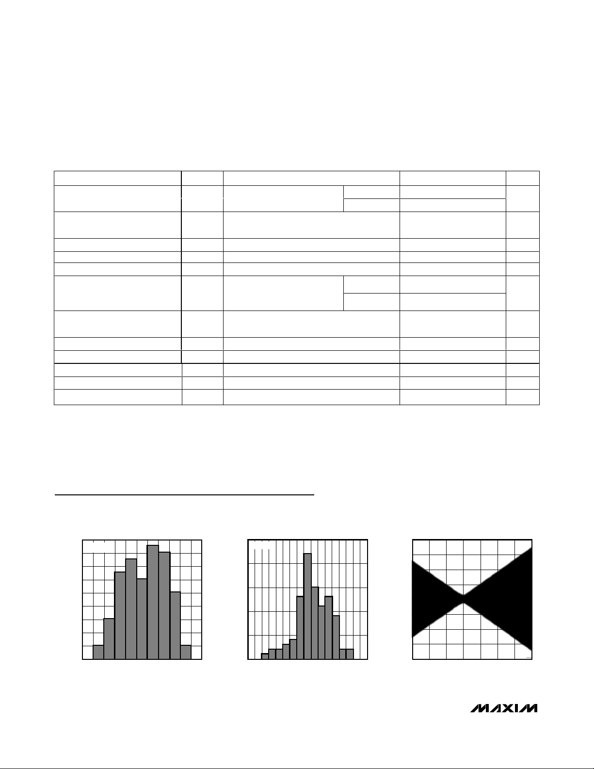
TCVOS DISTRIBUTION
0 0.5 1.0 1.5 2.0
-0.5
TCVOS (µV/°C)
MAX4236 toc02
OFFSET VOLTAGE vs. TEMPERATURE
80
60
40
20
0
-20
OFFSET VOLTAGE (µV)
-40
-60
-80
-50 0 25-25
TEMPERATURE (°C)
18
VOS DISTRIBUTION
VCC = 5V
16
14
12
10
8
6
PERCENT OF UNITS (%)
4
2
0
-10 -6 -4-8 -2 0 2 4 6 8 10
VOS (µV)
MAX 4236 toc01
PERCENT OF UNITS (%)
25
20
15
10
5
0
-
0.3 x V
50
V
CC
V
75 100 125
MAX4236 toc02

MAX4236/MAX4237
SOT23, Very High Precision, 3V/5V
Rail-To-Rail Op Amps
_______________________________________________________________________________________ 7
Typical Operating Characteristics (continued)
(VCC= +5V, VEE= 0, VCM= VCC/2, RL= 100kΩ to VCC/2, TA= +25°C, unless otherwise noted.)
COMMON-MODE REJECTION RATIO
vs. COMMON-MODE INPUT VOLTAGE
140
VCC = 3V
120
100
80
60
40
20
COMMON-MODE REJECTION RATIO (dB)
0
03.0
COMMON-MODE INPUT VOLTAGE (V)
2.0 2.51.51.00.5
MAX4236 toc04
COMMON-MODE REJECTION RATIO
140
vs. FREQUENCY (V
120
100
80
60
40
20
COMMON-MODE REJECTION RATIO (dB)
0
0.01 10 100 10000.1 1 10,000
FREQUENCY (kHz)
CC
= 3V)
MAX4236 toc07
COMMON-MODE REJECTION RATIO
vs. COMMON-MODE INPUT VOLTAGE
140
VCC = 5V
120
100
80
60
40
20
COMMON-MODE REJECTION RATIO (dB)
0
021345
COMMON-MODE INPUT VOLTAGE (V)
POWER-SUPPLY REJECTION RATIO
vs. FREQUENCY (V
120
100
80
60
PSSR (dB)
40
20
0
0.1 1 10 100 1000 10,000
MAX4236
OPEN-LOOP GAIN/PHASE
vs. FREQUENCY
140
120
100
GAIN
80
60
GAIN (dB)
40
VCC = 5V/3V
20
-20
= 15pF/200pF
C
L
0
0.001 10 10000.10.01 1 100 10,000
FREQUENCY (kHz)
MAX4236 toc10
PHASE
100
80
60
40
PHASE (DEGREES)
20
0
INPUT VOLTAGE NOISE vs. FREQUENCY
25
20
15
10
INPUT VOLTAGE NOISE (nV√Hz)
5
0
0.01 1 100.1 100
FREQUENCY (kHz)
FREQUENCY (kHz)
CC
= 5V)
COMMON-MODE REJECTION RATIO
vs. FREQUENCY (V
120
100
MAX4236 toc05
80
60
40
20
COMMON-MODE REJECTION RATIO (dB)
0
0.01 10 100 10000.1 1 10,000
OPEN-LOOP GAIN/PHASE
140
120
MAX4236 toc08
100
GAIN
80
60
GAIN (dB)
40
VCC = 5V/3V
20
-20
= 15pF/200pF
C
L
0
0.001 10 10000.10.01 1 100 10,000 100,000
TOTAL HARMONIC DISTORTION
PLUS NOISE vs. FREQUENCY
1
= 2Vp-p
V
OUT
MAX4236 toc11
0.1
0.01
THD + NOISE (%)
0.001
0.0001
10 100 10k 100k
FREQUENCY (kHz)
MAX4237
vs. FREQUENCY
FREQUENCY (kHz)
1k
FREQUENCY (Hz)
CC
= 5V)
MAX4236 toc09
PHASE
MAX4236 toc06
100
80
60
40
PHASE (DEGREES)
20
0
MAX4236 toc12

MAX4236/MAX4237
SOT23, Very High Precision, 3V/5V
Rail-To-Rail Op Amps
8 _______________________________________________________________________________________
Typical Operating Characteristics (continued)
(VCC= +5V, VEE= 0, VCM= VCC/2, RL= 100kΩ to VCC/2, TA= +25°C, unless otherwise noted.)
315
325
320
335
330
340
345
2.5 3.5 4.03.0 4.5 5.0 5.5
SUPPLY CURRENT vs. SUPPLY VOLTAGE
MAX4236 toc14
SUPPLY VOLTAGE (V)
SUPPLY CURRENT (µA)
TA = -40°C
TA = +25°C
T
A
= +85°C
T
A
= +125°C
60
80
100
120
LARGE-SIGNAL GAIN vs. TEMPERATURE
MAX4236 toc15
TEMPERATURE (°C)
GAIN (dB)
140
-50 25 50-25 0 75 100 125
VCC = 5V, RL to V
EE
VCC = 5V, RL to V
CC
VCC = 3V, RL to V
EE
VCC = 3V, RL to V
CC
RL = 1k
Ω
0
15
10
5
25
20
45
40
35
30
50
-50 -25 0 25 50 75 100 125
MINIMUM OUTPUT VOLTAGE
vs. TEMPERATURE
MAX4236 toc16
TEMPERATURE (°C)
MINIMUM OUTPUT VOLTAGE (mV)
VCC = 5V, RL = 1k
Ω
V
CC
= 3V, RL = 1k
Ω
VCC = 5V/3V, RL = 100k
Ω
0
60
40
20
100
80
180
160
140
120
200
-50 -25 0 25 50 75 100 125
MAXIMUM OUTPUT VOLTAGE
vs. TEMPERATURE
MAX4236 toc17
TEMPERATURE (°C)
MAXIMUM OUTPUT VOLTAGE (mV)
VCC = 5V, RL = 1k
Ω
V
CC
= 3V, RL = 1k
Ω
VCC = 5V/3V, RL = 100k
Ω
0
60
40
20
80
100
120
140
160
180
200
3.0 3.5 4.0 4.5 5.0
OUTPUT VOLTAGE
vs. SUPPLY VOLTAGE
MAX4236 toc18
SUPPLY VOLTAGE (V)
OUTPUT VOLTAGE (mV)
RL = 1k
Ω
VOL - V
EE, RL to VEE
VCC - V
OH, RL to VCC
0
0.5
1.0
1.5
2.0
2.5
3.0
3.5
4.0
3.0 3.5 4.0 4.5 5.0
OUTPUT VOLTAGE
vs. SUPPLY VOLTAGE
MAX4236 toc19
SUPPLY VOLTAGE (V)
OUTPUT VOLTAGE (mV)
VOL - V
EE
VCC - V
OH
RL = 100k
Ω
0
6
4
2
8
10
12
0 2.01.50.5 1.0 2.5 3.0 3.5 4.0 4.5 5.0
OUTPUT SOURCE CURRENT
vs. OUTPUT VOLTAGE
MAX4236 toc20
OUTPUT VOLTAGE (V)
OUTPUT SOURCE CURRENT (mA)
VCC = 5V
0
3
2
1
4
5
6
7
8
9
10
0 1.00.5 1.5 2.0 2.5 3.0
OUTPUT SOURCE CURRENT
vs. OUTPUT VOLTAGE
MAX4236 toc21
OUTPUT VOLTAGE (V)
OUTPUT SOURCE CURRENT (mA)
VCC = 3V
SUPPLY CURRENT vs. TEMPERATURE
400
390
380
370
360
350
340
330
SUPPLY CURRENT (µA)
320
310
300
+V = 5V
+V = 3V
-50 -25 0 25 50 75 100 125
TEMPERATURE (°C)
MAX4236 toc13

MAX4236/MAX4237
SOT23, Very High Precision, 3V/5V
Rail-To-Rail Op Amps
_______________________________________________________________________________________ 9
Typical Operating Characteristics (continued)
(VCC= +5V, VEE= 0, VCM= VCC/2, RL= 100kΩ to VCC/2, TA= +25°C, unless otherwise noted.)
SHORT-CIRCUIT CURRENT
vs. TEMPERATURE
MAX4236 toc25
0
5
15
10
30
35
25
20
40
SHORT-CIRCUIT CURRENT (mA)
-50 0 25-25
50
75 100 125
TEMPERATURE (°C)
VCC = 5V
VCC = 3V
SHORTED TO V
CC
(SINKING CURRENT)
-2.5
-1.0
-1.5
-2.0
-0.5
0
0.5
1.0
1.5
2.0
2.5
-100 -50 0 50 100
DC I/O TRANSFER CURVE
(R
LOAD
= 100kΩ)
MAX4236 toc26
DIFFERENTIAL INPUT VOLTAGE (µV)
OUTPUT VOLTAGE (V)
V
SUPPLY
= ±2.5V
-2.5
-1.0
-1.5
-2.0
-0.5
0
0.5
1.0
1.5
2.0
2.5
-100 -50 0 50 100
DC I/O TRANSFER CURVE
(R
LOAD
= 1kΩ)
MAX4236 toc27
DIFFERENTIAL INPUT VOLTAGE (µV)
OUTPUT VOLTAGE (V)
V
SUPPLY
= ±2.5V
1µs/div
MAX4236
NONINVERTING SMALL-SIGNAL RESPONSE
INPUT
10mV/div
OUTPUT
10mV/div
MAX4236 toc28
VCC = ±2.5V
R
L
= 1kΩ, CL = 15pF
A
V
= 1V/V
0
0
1µs/div
MAX4237
NONINVERTING SMALL-SIGNAL RESPONSE
INPUT
10mV/div
OUTPUT
50mV/div
MAX4236 toc29
VCC = ±2.5V
R
L
= 1kΩ, CL = 15pF
A
V
= 5V/V
0
0
OUTPUT SINK CURRENT
vs. OUTPUT VOLTAGE
80
70
60
50
40
30
20
OUTPUT SINK CURRENT (mA)
10
0
0 1.0 1.5 2.0 2.50.5 3.0 3.5 4.0 4.5 5.0
VCC = 5V
OUTPUT TO GND
60
MAX4236 toc22
50
40
30
20
OUTPUT SINK CURRENT (mA)
10
0
OUTPUT SINK CURRENT
vs. OUTPUT VOLTAGE
VCC = 3V
OUTPUT TO GND
0 1.0 1.50.5 2.0 2.5 3.0
OUTPUT VOLTAGE (V)
20
MAX4236 toc23
15
10
5
SHORT-CIRCUIT CURRENT (mA)
SHORTED TO V
(SOURCING CURRENT)
0
-50 25 50-25 0 75 100 125
SHORT-CIRCUIT CURRENT
vs. TEMPERATURE
MAX4236 toc24
VCC = 5V
VCC = 3V
EE
TEMPERATURE (°C)

MAX4236/MAX4237
SOT23, Very High Precision, 3V/5V
Rail-To-Rail Op Amps
10 ______________________________________________________________________________________
Typical Operating Characteristics (continued)
(VCC= +5V, VEE= 0, VCM= VCC/2, RL= 100kΩ to VCC/2, TA= +25°C, unless otherwise noted.)
NONINVERTING LARGE-SIGNAL RESPONSE
0
0
VCC = ±2.5V
= 1k
R
Ω,
L
= 5V/V
A
V
2µs/div
CL = 15pF
MAX4236 toc30
MAX4236
MAX4237
NONINVERTING LARGE-SIGNAL RESPONSE
0
MAX4236 toc32
INPUT
200mV/div
OUTPUT
1V/div
INPUT
1V/div
NONINVERTING LARGE-SIGNAL RESPONSE
0
0
VCC = ±2.5V
= 100k
R
L
= 5V/V
A
V
CL = 15pF
Ω,
1µs/div
MAX4236 toc31
MAX4236
MAX4237
NONINVERTING LARGE-SIGNAL RESPONSE
0
MAX4236 toc33
INPUT
200mV/div
OUTPUT
1V/div
INPUT
1V/div
OUTPUT
1V/div
0
VCC = ±2.5V
R
L
A
V
= 1k
= 1V/V
Ω,
4µs/div
CL = 15pF
0
VCC = ±2.5V
= 100k
R
L
= 1V/V
A
V
Ω,
4µs/div
CL = 15pF
OUTPUT
1V/div

MAX4236/MAX4237
SOT23, Very High Precision, 3V/5V
Rail-To-Rail Op Amps
______________________________________________________________________________________ 11
Detailed Description
The MAX4236/MAX4237 are high-precision op amps
with a CMOS input stage and an excellent set of DC
and AC features. The combination of tight maximum
voltage offset, low offset tempco and very low input
current make them ideal for use in high-precision DC
circuits. They feature low-voltage operation, low-power
consumption, high-current drive with rail-to-rail output
swing and high-gain bandwidth product.
High Accuracy
The MAX4236/MAX4237 maximum input offset voltage
is 20µV (5µV, typ) for grade A version and 50µV for
grade B version at +25°C. The maximum temperature
coefficient of the offset voltage for grade A and B are
guaranteed to be 2µV/°C and 4.5µV/°C respectively.
The parts have an input bias current of 1pA. Noise
characteristics are 14nV/√Hz, and a low frequency
noise (0.1Hz to 10Hz) of 0.2µVp-p. The CMRR is
102dB, and the PSRR is 120dB. The combination is
what is necessary for the design of circuits to process
signals while keeping high signal-to-noise ratios, as in
stages preceding high-resolution converters, or when
they are produced by sensors or transducers generating very small outputs.
Rail-to-Rail Outputs, Ground-Sensing Input
The input common-mode range extends from (VEE-
0.15V) to (VCC- 1.2V) with excellent common-mode
rejection. Beyond this range, the amplifier output is a
nonlinear function of the input, but does not undergo
phase reversal or latch-up (see Typical Operating
Characteristics).
The output swings to within 150mV of the power-supply
rails with a 1kΩ load. The input ground sensing and the
rail-to-rail output substantially increase the dynamic
range.
Power-Up and Shutdown Mode
The MAX4236/MAX4237 have a shutdown option.
When the shutdown pin (SHDN) is pulled low, the supply current drops to 0.1µA, and the amplifiers are disabled with the output in a high-impedance state. Pulling
SHDN high enables the amplifiers. The turn-on time for
the amplifiers to come out of shutdown is 4µs.
Applications Information
As described above, the characteristics of the
MAX4236/MAX4237 are excellent for high-precision/
accuracy circuitry, and the high impedance, low-current, low-offset, and noise specifications are very
attractive for piezoelectric transducers applications. In
these applications, the sensors generate an amount of
electric charge proportional to the changes in the
mechanical stress applied to them. These charges are
transformed into a voltage proportional to the applied
force by injecting them into a capacitance and then
amplifying the resulting voltage. The voltage is an
inverse function of the capacitance into which the
charges generated by the transducer/ sensor are
injected. This capacitance and the resistance that discharges it, define the low-frequency response of the
circuit. It is desirable, once the preferred low-frequency
response is known, to maintain the capacitance as low
as possible, because the amount of necessary
upstream amplification (and the signal-to-noise ratio
deterioration) is directly proportional to the capacitance
value. The MAX4236/MAX4237 high-impedance, low-
Pin Description
PIN
SOT23 SO/µMAX
1 6 OUT Amplifier Output
24V
3 3 IN+ Noninverting Amplifier Input
4 2 IN- Inverting Amplifier Input
58SHDN
67V
— 1, 5 N.C. No Connection. Not internally connected.
NAME FUNCTION
EE
CC
Negative Power Supply. Bypass with a 0.1µF capacitor to ground. Connect to GND
for single-supply operation.
Shutdown Input. Do not leave floating. Connect to V
to enter the shutdown mode.
Positive Supply Input. Bypass with a 0.1µF capacitor to ground.
for normal operation or GND
CC
MAX4236/MAX4237
SOT23, Very High Precision, 3V/5V
Rail-To-Rail Op Amps
12 ______________________________________________________________________________________
current, low-noise inputs allow a minimum of capacitance to be used.
Piezoresistive transducers applications require many of
the same qualities. For those applications the
MAX4236/MAX4237 high CMRR, PSRR, and offset stability are also a good match.
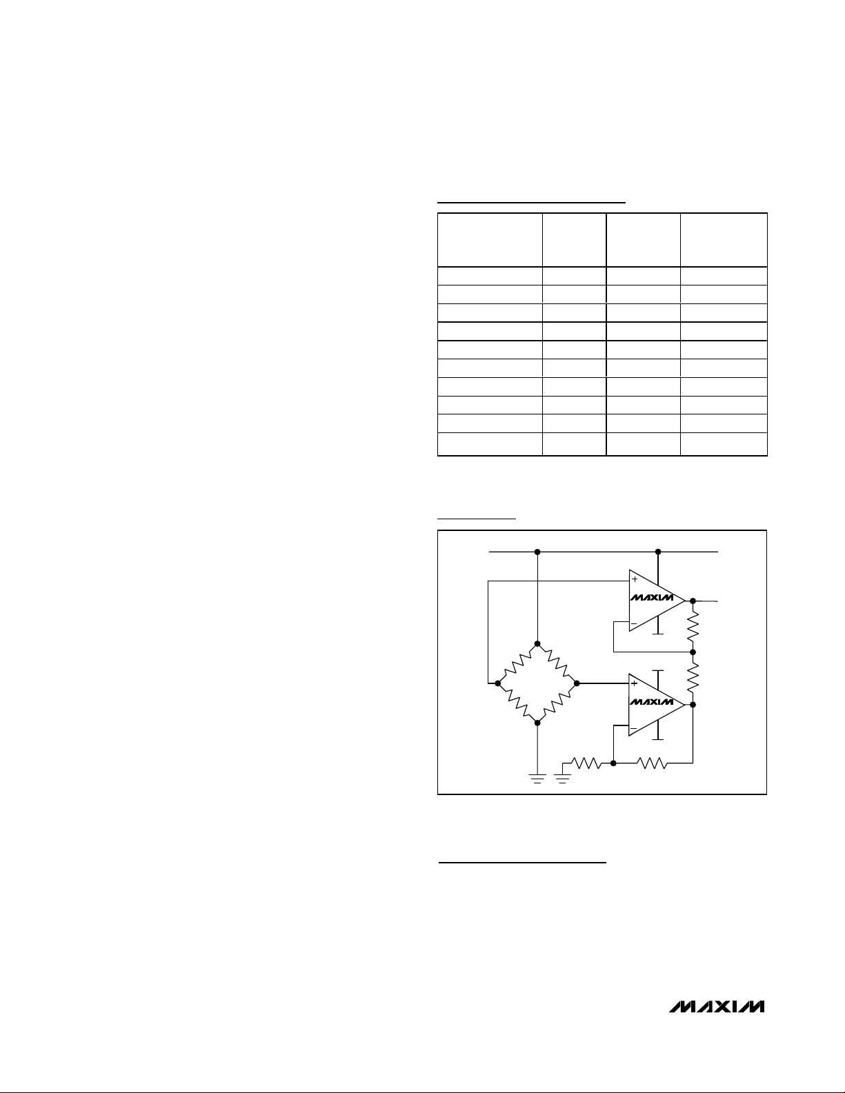
A typical application for a piezoresistive transducer
instrumentation amplifier design using the
MAX4236/MAX4237 is shown in the Typical Application
Circuit.
In general, the MAX4236/MAX4237 are good components for any application in which an amplifier with an
almost zero input current is required, including highprecision, long time-constant integrators and electrochemical sensors.
Power Supplies
The MAX4236/MAX4237 can operate from a single
+2.4V to +5.5V power supply, or from ±1.2V to ±2.75V
power supplies. The power supply pin(s) must be
bypassed to ground with a 0.1µF capacitor as close to
the pin as possible.
Layout and Physical Design
A good layout improves performance by decreasing
the amount of parasitic and stray capacitance, inductance and resistance at the amplifier’s inputs, outputs,
and power-supply connections. Since parasitics might
be unavoidable, minimize trace lengths, resistor leads,
and place external components as close to the pins as
possible.
In high impedance, low input current applications, input
lines guarding and shielding, special grounding, and
other physical design and layout techniques, are
mandatory if good results are expected.
The negative effects of crosstalk, EMI and other forms
of interference and noise (thermal, acoustic, etc.) must
be accounted for and prevented beforehand for good
performance in the type of sensitive circuitry in which
the MAX4236/MAX4237 are likely to be used.
Selector Guide
Typical Application Circuit
Chip Information
TRANSISTOR COUNTS: 224
PROCESS: BiCMOS
MINIMUM
PART GRADE
MAX4236EUT — 1 AAUV
MAX4236AEUA A 1 —
MAX4236BEUA B 1 —
MAX4236AESA A 1 —
MAX4236BESA B 1 —
MAX4237EUT — 5 AAUW
MAX4237AEUA A 5 —
MAX4237BEUA B 5 —
MAX4237AESA A 5 —
MAX4237BESA B 5 —
STABLE
GAIN
TOP MARK
+V
S
V
OUT
LOAD CELL
MAX4236
-V
+V
MAX4236
-V
S
S
S

MAX4236/MAX4237
SOT23, Very High Precision, 3V/5V
Rail-To-Rail Op Amps
______________________________________________________________________________________ 13
Package Information
6LSOT.EPS
8LUMAXD.EPS
MAX4236/MAX4237
SOT23, Very High Precision, 3V/5V
Rail-To-Rail Op Amps
Maxim cannot assume responsibility for use of any circuitry other than circuitry entirely embodied in a Maxim product. No circuit patent licenses are
implied. Maxim reserves the right to change the circuitry and specifications without notice at any time.
14 ____________________Maxim Integrated Products, 120 San Gabriel Drive, Sunnyvale, CA 94086 408-737-7600
© 2001 Maxim Integrated Products Printed USA is a registered trademark of Maxim Integrated Products.
Package Information (continued)
SOICN.EPS
 Loading...