

Datasheet MAX4228EUB, MAX4228ESD, MAX4226ESDB, MAX4225ESA, MAX4224EUT-T Datasheet (Maxim)
...
_______________General Description
The MAX4223–MAX4228 current-feedback amplifiers
combine ultra-high-speed performance, low distortion,
and excellent video specifications with low-power operation. The MAX4223/MAX4224/MAX4226/MAX4228
have a shutdown feature that reduces power-supply
current to 350µA and places the outputs into a highimpedance state. These devices operate with dual supplies ranging from ±2.85V to ±5.5V and provide a
typical output drive current of 80mA. The MAX4223/
MAX4225/MAX4226 are optimized for a closed-loop
gain of +1 (0dB) or more and have a -3dB bandwidth of
1GHz, while the MAX4224/MAX4227/MAX4228 are
compensated for a closed-loop gain of +2 (6dB) or
more, and have a -3dB bandwidth of 600MHz (1.2GHz
gain-bandwidth product).
The MAX4223–MAX4228 are ideal for professional video
applications, with differential gain and phase errors of
0.01% and 0.02°, 0.1dB gain flatness of 300MHz, and a
1100V/µs slew rate. Total harmonic distortion (THD) of
-60dBc (10MHz) and an 8ns settling time to 0.1% suit
these devices for driving high-speed analog-to-digital
inputs or for data-communications applications. The lowpower shutdown mode on the MAX4223/MAX4224/
MAX4226/MAX4228 makes them suitable for portable
and battery-powered applications. Their high output
impedance in shutdown mode is excellent for multiplexing applications.
The single MAX4223/MAX4224 are available in spacesaving 6-pin SOT23 packages. All devices are available
in the extended -40°C to +85°C temperature range.
________________________Applications
ADC Input Buffers Data Communications
Video Cameras Video Line Drivers
Video Switches Video Multiplexing
Video Editors XDSL Drivers
RF Receivers Differential Line Drivers
____________________________Features
♦ Ultra-High Speed and Fast Settling Time:
1GHz -3dB Bandwidth (MAX4223, Gain = +1)
600MHz -3dB Bandwidth (MAX4224, Gain = +2)
1700V/µs Slew Rate (MAX4224)
5ns Settling Time to 0.1% (MAX4224)
♦ Excellent Video Specifications (MAX4223):
Gain Flatness of 0.1dB to 300MHz
0.01%/0.02° DG/DP Errors
♦ Low Distortion:
-60dBc THD (f
c
= 10MHz)
42dBm Third-Order Intercept (f = 30MHz)
♦ 6.0mA Quiescent Supply Current (per amplifier)
♦ Shutdown Mode:
350µA Supply Current (per amplifier)
100kΩ Output Impedance
♦ High Output Drive Capability:
80mA Output Current
Drives up to 4 Back-Terminated 75Ω Loads to
±2.5V while Maintaining Excellent Differential
Gain/Phase Characteristics
♦ Available in Tiny 6-Pin SOT23 and 10-Pin µMAX
Packages
MAX4223–MAX4228
1GHz, Low-Power, SOT23,
Current-Feedback Amplifiers with Shutdown
________________________________________________________________
Maxim Integrated Products
1
V
EE
IN-
IN+
1
6
V
CC
5
SHDN
OUT
MAX4223
MAX4224
SOT23-6
TOP VIEW
2
3
4
_________________Pin Configurations
19-1230; Rev 2a; 6/97
PART
MAX4223EUT-T
MAX4223ESA -40°C to +85°C
-40°C to +85°C
TEMP. RANGE
PIN-
PACKAGE
6 SOT23
8 SO
EVALUATION KIT
AVAILABLE
______________Ordering Information
_____________________Selector Guide
Pin Configurations
continued at end
of data sheet.
Ordering Information continued at end of data sheet.
For free samples & the latest literature: http://www.maxim-ic.com, or phone 1-800-998-8800
For small orders, phone 408-737-7600 ext. 3468.
SOT
TOP MARK
AAAD
—
10 µMAX,
14 SO
8 SO
10 µMAX,
14 SO
8 SO
6 SOT23, 8 SO
6 SOT23, 8 SO
PIN-
PACKAGE
Yes
No
Yes
No
Yes
Yes
SHUTDOWN
MODE
2
2
2
2
1
1
AMPS
PER
PKG.
2
2MAX4227
MAX4228
1
PART
1MAX4225
MAX4226
2
1MAX4223
MAX4224
MIN.
GAIN
MAX4223–MAX4228
1GHz, Low-Power, SOT23,
Current-Feedback Amplifiers with Shutdown
2 _______________________________________________________________________________________
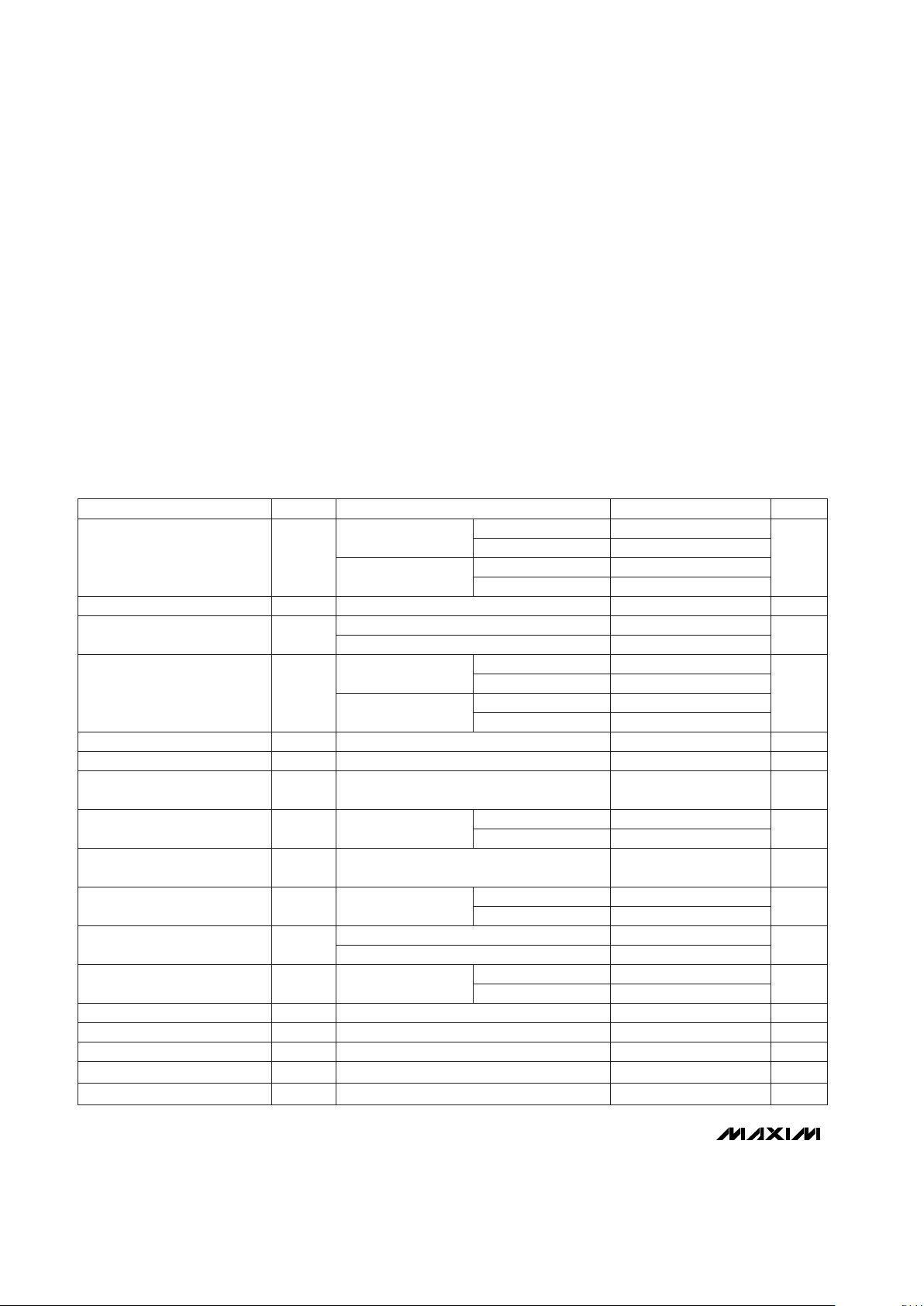
ABSOLUTE MAXIMUM RATINGS
DC ELECTRICAL CHARACTERISTICS
(VCC= +5V, VEE= -5V, SHDN = 5V, VCM= 0V, RL= ∞, TA= T
MIN
to T
MAX
, unless otherwise noted. Typical values are at
T
A
= +25°C.) (Note 1)
Stresses beyond those listed under “Absolute Maximum Ratings” may cause permanent damage to the device. These are stress ratings only, and functional
operation of the device at these or any other conditions beyond those indicated in the operational sections of the specifications is not implied. Exposure to
absolute maximum rating conditions for extended periods may affect device reliability.
Supply Voltage (VCCto VEE)..................................................12V
Analog Input Voltage .......................(V
EE
- 0.3V) to (VCC+ 0.3V)
Analog Input Current........................................................±25mA
SHDN Input Voltage.........................(V
EE
- 0.3V) to (VCC+ 0.3V)
Short-Circuit Duration
OUT to GND...........................................................Continuous
OUT to V
CC
or VEE............................................................5sec
Continuous Power Dissipation (T
A
= +70°C)
6-Pin SOT23 (derate 7.1mW/°C above +70°C).............571mW
8-Pin SO (derate 5.9mW/°C above +70°C)...................471mW
10-Pin µMAX (derate 5.6mW/°C above +70°C)............444mW
14-Pin SO (derate 8.3mW/°C above +70°C).................667mW
Operating Temperature Range ...........................-40°C to +85°C
Storage Temperature Range.............................-65°C to +150°C
Lead Temperature (soldering, 10sec).............................+300°C
CONDITIONS
±0.5 ±4
UNITSMIN TYP MAXSYMBOLPARAMETER
mV
±0.5 ±5
V
OS
Input Offset Voltage
±2 ±10
Input Bias Current
(Positive Input)
±7
TA= T
MIN
to T
MAX
µA
±15
TA= +25°C
Ω45R
IN-
Input Resistance (Negative Input)
kΩ700R
IN+
Input Resistance (Positive Input)
55 61
Inferred from CMRR test V±2.5 ±3.2V
CM
Input Common-Mode
Voltage Range
Inferred from PSRR test V±2.85 ±5.5VCC/V
EE
VCM= ±2.5V
Operating Supply Voltage
Range
68 74
dB
50
CMRRCommon-Mode Rejection Ratio
VCC= 2.85V to 5.5V,
VEE= -2.85V to -5.5V
dB
63
PSRRPower-Supply Rejection Ratio
Shutdown mode (SHDN = 0V)
mA
0.35 0.55
RL= 50Ω
I
SY
Quiescent Supply Current
(per Amplifier)
Normal mode (SHDN = 5V)
6.0 9.0
V±2.5 ±2.8V
OUT
Output Voltage Swing
V
OUT
= ±2.5V MΩ
0.3 0.8
T
R
Open-Loop Transresistance
V
OUT
= ±2.5V mA60 80I
OUT
Output Current (Note 2)
0.7 1.5
RL= short to ground mA140I
SC
Short-Circuit Output Current
V0.8V
IL
SHDN Logic Low
±4 ±20
TA= +25°C
µA
±4 ±25
I
B+
TA= +25°C
TA= T
MIN
to T
MAX
TA= +25°C
TA= T
MIN
to T
MAX
RL= ∞
RL= 50Ω
V2.0V
IH
SHDN Logic High
±6
TA= T
MIN
to T
MAX
MAX4223/MAX4224
MAX4223/MAX4224
MAX4225–MAX4228
µV/°C±2TCV
OS
Input Offset Voltage Drift
MAX4225–MAX4228
TA= T
MIN
to T
MAX
±30
Input Bias Current
(Negative Input)
±35
I
B-
TA= +25°C
MAX4223/MAX4224
MAX4225–MAX4228
MAX4223/MAX4224
MAX4225–MAX4228
MAX4223–MAX4228
1GHz, Low-Power, SOT23,
Current-Feedback Amplifiers with Shutdown
_______________________________________________________________________________________ 3
DC ELECTRICAL CHARACTERISTICS (continued)
(VCC= +5V, VEE= -5V, SHDN = 5V, VCM= 0V, RL= ∞, TA= T
MIN
to T
MAX
, unless otherwise noted. Typical values are at
T
A
= +25°C.) (Note 1)
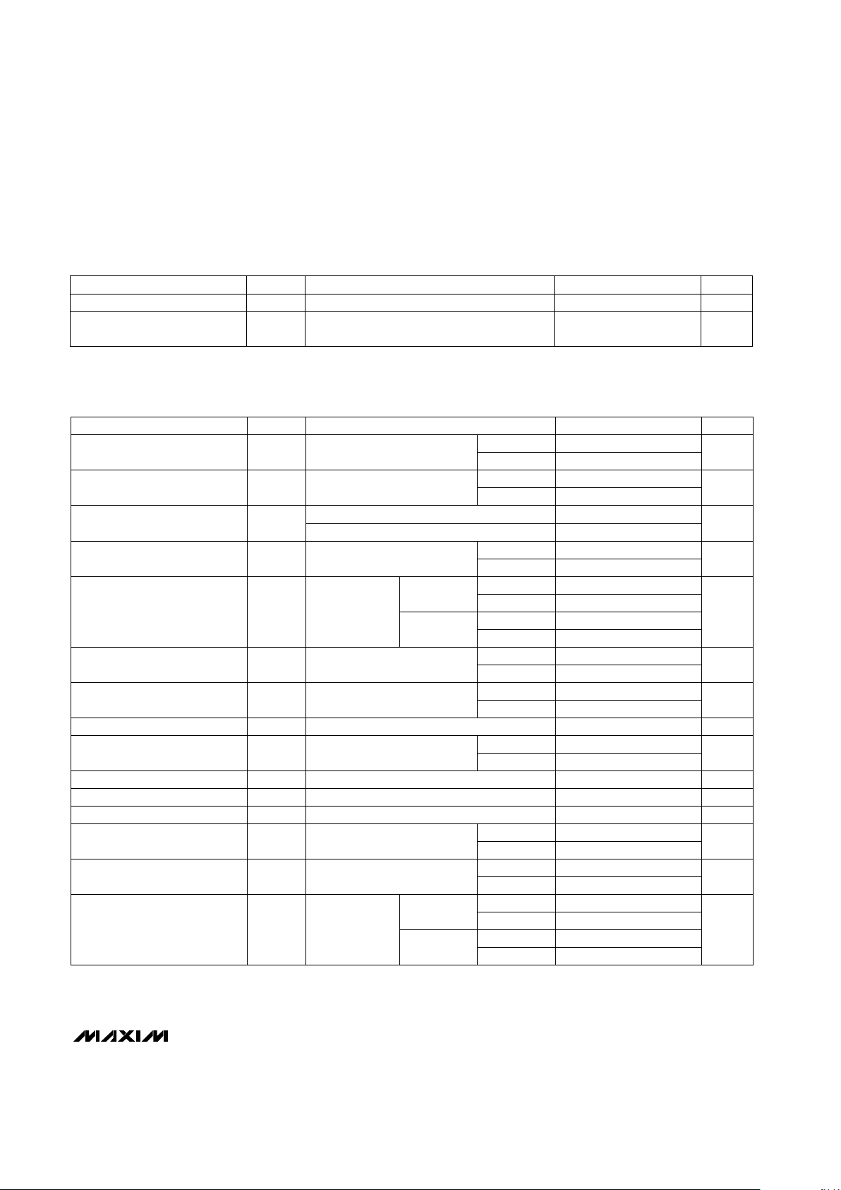
AC ELECTRICAL CHARACTERISTICS
(VCC= +5V, VEE= -5V, SHDN = 5V, VCM= 0V, AV= +1V/V for MAX4223/MAX4225/MAX4226, AV= +2V/V for MAX4224/MAX4227/
MAX4228, R
L
= 100Ω, TA= +25°C, unless otherwise noted.) (Note 4)
10 100
CONDITIONS
25 70
UNITSMIN TYP MAXSYMBOLPARAMETER
µAIIL/I
IH
SHDN Input Current SHDN = 0V or 5V
SHDN = 0V, V
OUT
= -2.5V to +2.5V
(Note 3)
Shutdown Mode Output
Impedance
kΩ
MAX4224/7/8
MAX4223/5/6
60 200
100 300
MAX4223/5/6
0.1
V
OUT
= 2V step
MAX4224/7/8
THD
850 1100
1.5
Total Harmonic Distortion
RL= 1kΩ
1400 1700
250
-65
V
OUT
= 4V step
625 800
dB
CONDITIONS
Gain Peaking
V
OUT
= 2Vp-p MHz
330
BW
LS
Large-Signal Bandwidth
MAX4223/4/6/8
V
OUT
= 2V step
RL= 100Ω
MAX4223/5/6
MAX4223/5/6
µs2
0.02
t
ON
Turn-On Time from Shutdown
SHDN = 0V, f = 10MHz, MAX4223/4/6/8
dB65Off Isolation
RL= 150Ω (Note 6)
0.01
degrees
0.01
VCC, VEE= 0V to ±5V step ns100t
UP
MAX4223/4/6/8
Power-Up Time
RL= 150Ω (Note 6) %
0.02
DGDifferential Gain Error
ns300t
OFF
Turn-Off Time to Shutdown
f = 30MHz,
RS= 50Ω
MAX4225/6
-60
325 600
dBc
-61
MAX4223/5/6
750 1000
MAX4224/7/8
-78
MAX4224/7/8
DPDifferential Phase Error
MAX4224/7/8
MAX4224/7/8
MAX4223/5/6
MAX4223/5/6
Rising edge
MAX4223/5/6
V
OUT
= 2Vp-p,
fC= 10MHz
MAX4224/7/8
MAX4223/5/6
1.0
Falling edge
1100 1400
V/µsSRSlew Rate (Note 5)
MAX4224/7/8
1.5
UNITSMIN TYP MAXSYMBOLPARAMETER
ns
MAX4224/7/8
tr, t
f
Rise and Fall Time
MAX4223/5/6
MAX4223/5/6
MAX4224/7/8
MAX4223/5/6
V
OUT
= 20mVp-p MHz
MAX4224/7/8
BW
0.1dB
Bandwidth for ±0.1dB
Gain Flatness (Note 5)
V
OUT
= 20mVp-p
-72
MAX4227/8
-68
8
dB
ns
5
X
TALK
t
S
Settling Time to 0.1%
Crosstalk
MHzBW
-3dB Small-Signal Bandwidth
(Note 5)
MAX4224/7/8

MAX4223–MAX4228
1GHz, Low-Power, SOT23,
Current-Feedback Amplifiers with Shutdown
4 _______________________________________________________________________________________
Note 1: The MAX422_EUT is 100% production tested at TA= +25°C. Specifications over temperature limits are guaranteed by design.
Note 2: Absolute Maximum Power Dissipation must be observed.
Note 3: Does not include impedance of external feedback resistor network.
Note 4: AC specifications shown are with optimal values of R
F
and RG. These values vary for product and package type, and are
tabulated in the
Applications Information
section of this data sheet.
Note 5: The AC specifications shown are not measured in a production test environment. The minimum AC specifications given are
based on the combination of worst-case design simulations along with a sample characterization of units. These minimum
specifications are for design guidance only and are not intended to guarantee AC performance (see
AC Testing/
Performance
). For 100% testing of these parameters, contact the factory.
Note 6: Input Test Signal: 3.58MHz sine wave of amplitude 40IRE superimposed on a linear ramp (0IRE to 100IRE). IRE is a unit of
video signal amplitude developed by the International Radio Engineers. 140IRE = 1V.
Note 7: Assumes printed circuit board layout similar to that of Maxim’s evaluation kit.
AC ELECTRICAL CHARACTERISTICS (continued)
(VCC= +5V, VEE= -5V, SHDN = 5V, VCM= 0V, AV= +1V/V for MAX4223/MAX4225/MAX4226, AV= +2V/V for MAX4224/MAX4227/
MAX4228, R
L
= 100Ω, TA= +25°C, unless otherwise noted.) (Note 4)
__________________________________________Typical Operating Characteristics
(VCC= +5V, VEE= -5V, RL= 100Ω, TA = +25°C, unless otherwise noted.)
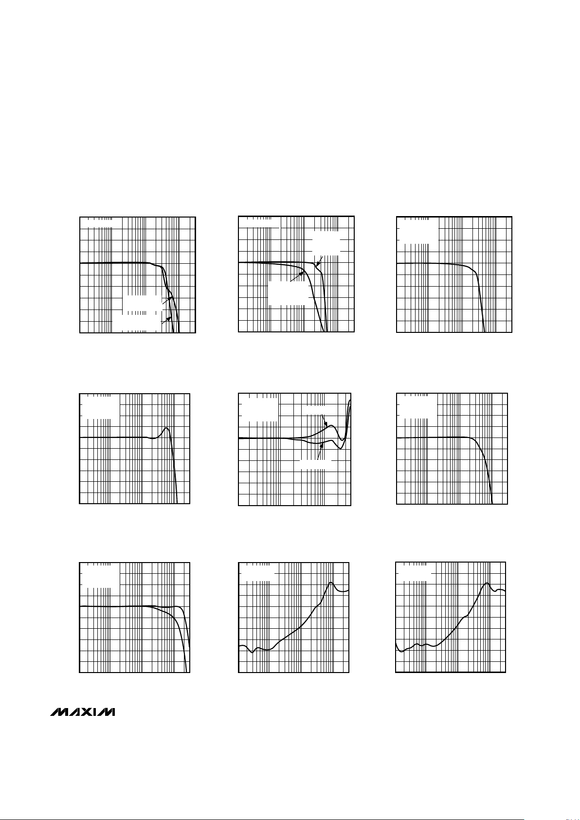
4
3
-6
1 100 100010
MAX4223
SMALL-SIGNAL GAIN vs. FREQUENCY
(A
VCL
= +1)
-4
-5
MAX4223-01
FREQUENCY (MHz)
GAIN (dB)
-2
-3
0
-1
2
1
VIN = 20mVp-p
SO-8 PACKAGE
R
F
= 560Ω
SOT23-6
R
F
= 470Ω
4
3
-6
1 100 100010
MAX4223
SMALL-SIGNAL GAIN vs. FREQUENCY
(A
VCL
= +2/+5)
-4
-5
MAX4223-02
FREQUENCY (MHz)
NORMALIZED GAIN (dB)
-2
-3
0
-1
2
1
VIN = 20mVp-p
AV = +2V/V
R
F
= RG = 200Ω
AV = +5V/V
R
F
= 100Ω
R
G
= 25Ω
4
3
-6
1 100 100010
MAX4223/MAX4225/MAX4226
LARGE-SIGNAL GAIN vs. FREQUENCY
(A
VCL
= +1)
-4
-5
MAX4223-03
FREQUENCY (MHz)
GAIN (dB)
-2
-3
0
-1
2
1
A
V
= +1V/V
R
F
= 560Ω
V
OUT
= 2Vp-p
PARAMETER SYMBOL MIN TYP MAX UNITS
Input Capacitance (Note 7) C
IN
0.8
42
Third-Order Intercept IP3
36
1.0
dBm
SO-8, SO-14
packages
f = 30kHz
fz= 30.1MHz
SOT23-6, 10-pin µMAX
packages
0.3
0.3
CONDITIONS
2Output Impedance Z
OUT
Ω
201dB Gain Compression
2
dBmf = 10kHz
f = 10kHz
3
Input Noise Current Density in+, in-
20
pA/√Hz
f = 10kHz
Input Noise Voltage Density
pF
e
n
nV/√Hz
f = 10kHz
MAX4223/5/6
MAX4224/7/8
-61
Spurious-Free Dynamic Range SFDR
-62
dBf = 10kHz
MAX4223/5/6
MAX4224/7/8
IN+
INPin to pin
Pin to GND
Pin to pin
Pin to GND
MAX4223–MAX4228
1GHz, Low-Power, SOT23,
Current-Feedback Amplifiers with Shutdown
_______________________________________________________________________________________
5
4
3
-6
1 100 100010
MAX4224
SMALL-SIGNAL GAIN vs. FREQUENCY
(A
VCL
= +2)
-4
-5
MAX4223-04
FREQUENCY (MHz)
NORMALIZED GAIN (dB)
-2
-3
0
-1
2
1
VIN = 20mVp-p
SO-8 PACKAGE
R
F
= RG = 470Ω
SOT23-6 PACKAGE
R
F
= RG = 470Ω
4
3
-6
1 100 100010
MAX4224
SMALL-SIGNAL GAIN vs. FREQUENCY
(A
VCL
= +5/+10)
-4
-5
MAX4223-05
FREQUENCY (MHz)
NORMALIZED GAIN (dB)
-2
-3
0
-1
2
1
VIN = 20mVp-p
A
VCL
= +5V/V
R
F
= 240Ω
R
G
= 62Ω
A
VCL
= +10V/V
R
F
= 130Ω
R
G
= 15Ω
4
3
-6
1 100 100010
MAX4224/MAX4227/MAX4228
LARGE-SIGNAL GAIN vs. FREQUENCY
(A
VCL
= +2)
-4
-5
MAX4223-06
FREQUENCY (MHz)
NORMALIZED GAIN (dB)
-2
-3
0
-1
2
1
A
VCL
= +2V/V
R
F
= RG = 470Ω
V
OUT
= 2Vp-p
4
3
-6
1 100 100010
MAX4225/MAX4226
SMALL-SIGNAL GAIN vs. FREQUENCY
(A
VCL
= +1)
-4
-5
MAX4223-07
FREQUENCY (MHz)
GAIN (dB)
-2
-3
0
-1
2
1
VIN = 20mVp-p
A
VCL
= +1V/V
R
F
= 560Ω
0.4
0.3
-0.6
0.1 10 1001
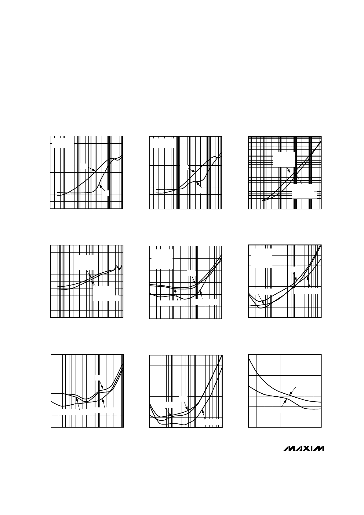
MAX4227/MAX4228
GAIN MATCHING vs. FREQUENCY
(A
VCL
= +2)
-0.4
-0.5
MAX4223-10
FREQUENCY (MHz)
NORMALIZED GAIN (dB)
-0.2
-0.3
0
-0.1
0.2
0.1
VIN = 20mVp-p
A
VCL
= +2V/V
R
F
= RG = 470Ω
10 100
MAX4225/MAX4226
GAIN MATCHING vs. FREQUENCY
(A
VCL
= +1)
MAX4223-08
FREQUENCY (MHz)
GAIN (dB)
1
AMPLIFIER A
0.4
0.3
-0.6
-0.4
-0.5
-0.2
-0.3
0
-0.1
0.2
0.1
VIN = 2OmVp-p
A
VCL
= +1V/V
R
F
= 560Ω
AMPLIFIER B
0
-10
-100
1 100 100010
MAX4225/MAX4226
CROSSTALK vs. FREQUENCY
-80
-90
MAX4223-11
FREQUENCY (MHz)
CROSSTALK (dB)
-60
-70
-40
-50
-20
-30
RS = 50Ω
V
OUT
= 2Vp-p
0
-10
-100
1 100 100010
MAX4227/MAX4228
CROSSTALK vs. FREQUENCY
-80
-90
MAX4223-12
FREQUENCY (MHz)
CROSSTALK (dB)
-60
-70
-40
-50
-20
-30
RS = 50Ω
V
OUT
= 2Vp-p
____________________________Typical Operating Characteristics (continued)
(VCC= +5V, VEE= -5V, RL= 100Ω, TA = +25°C, unless otherwise noted.)
4
3
-6
1 100 100010
MAX4227/MAX4228
SMALL-SIGNAL GAIN vs. FREQUENCY
(A
VCL
= +2)
-4
-5
MAX4223-09
FREQUENCY (MHz)
NORMALIZED GAIN (dB)
-2
-3
0
-1
2
1
VIN = 20mVp-p
A
VCL
= +2V/V
R
F
= RG = 470Ω
MAX4223–MAX4228
1GHz, Low-Power, SOT23,
Current-Feedback Amplifiers with Shutdown
6 _______________________________________________________________________________________
____________________________Typical Operating Characteristics (continued)
(VCC= +5V, VEE= -5V, RL= 100Ω, TA = +25°C, unless otherwise noted.)
10
0
-90
0.01 1 10 1000.1
MAX4223/MAX4225/MAX4226
POWER-SUPPLY REJECTION RATIO
vs. FREQUENCY (A
VCL
= +1)
-70
-80
MAX4223-13
FREQUENCY (MHz)
PSRR (dB)
-50
-60
-30
-40
-10
-20
A
VCL
= +1V/V
R
F
= 560Ω
V
CC
V
EE
10
0
-90
0.01 1 10 1000.1
MAX4224/MAX4227/MAX4228
POWER-SUPPLY REJECTION RATIO
vs. FREQUENCY (A
VCL
= +2)
-70
-80
MAX4223-14
FREQUENCY (MHz)
PSRR (dB)
-50
-60
-30
-40
-10
-20
A
VCL
= +2V/V
R
F
= RG = 470Ω
V
CC
V
EE
0.01
0.01 0.1 1 10 100
OUTPUT IMPEDANCE vs. FREQUENCY
0.1
MAX4223-15
FREQUENCY (MHz)
OUTPUT IMPEDANCE (Ω)
1
10
100
MAX4224/7/8
A
VCL
= +2V/V
R
F
= RG = 470Ω
MAX4223/5/6
A
VCL
= +1V/V
R
F
= 560Ω
20
-180
0.01 10 1000.1 1 1000
SHUTDOWN MODE OUTPUT ISOLATION
vs. FREQUENCY
-140
-160
MAX4223-16
FREQUENCY (MHz)
SHUTDOWN MODE OUTPUT ISOLATION (dB)
-100
-120
-60
-20
0
-40
-80
MAX4224/7/8
A
VCL
= +2V/V
R
F
= RG = 470Ω
MAX4223/5/6
A
VCL
= +1V/V
R
F
= 560Ω
-30
-90
0.1 10 100
MAX4224/MAX4227/MAX4228
TOTAL HARMONIC DISTORTION
vs. FREQUENCY (R
L
= 150Ω)
-70
-50
-40
-60
-80
MAX4223-19
FREQUENCY (MHz)
THD (dBc)
1
3RD HARMONIC
2ND HARMONIC
THD
-30
-90
0.1 10 100
MAX4223/MAX4225/MAX4226
TOTAL HARMONIC DISTORTION
vs. FREQUENCY (R
L
= 150Ω)
-70
-50
-40
-60
-80
MAX4223-17
FREQUENCY (MHz)
THD (dBc)
1
A
VCL
= +1V/V
R
L
= 150Ω
R
F
= 560Ω
V
OUT
= 2Vp-p
3RD HARMONIC
2ND HARMONIC
THD
-30
-100
0.1 10 100
MAX4223/MAX4225/MAX4226
TOTAL HARMONIC DISTORTION
vs. FREQUENCY (R
L
= 1kΩ)
-80
-60
-40
-70
-50
-90
MAX4223-18
FREQUENCY (MHz)
THD (dBc)
1
A
VCL
= +1V/V
R
L
= 1kΩ
R
F
= 560Ω
V
OUT
= 2Vp-p
2ND HARMONIC
3RD HARMONIC
THD
-30
-100
0.1 10 100
MAX4224/MAX4227/MAX4228
TOTAL HARMONIC DISTORTION
vs. FREQUENCY (R
L
= 1kΩ)
-80
-60
-40
-70
-50
-90
MAX4223-20
FREQUENCY (MHz)
THD (dBc)
1
2ND HARMONIC
3RD HARMONIC
THD
20
30
25
40
35
50
45
55
10 30 4020 50 60 70 80 90 100
TWO-TONE THIRD-ORDER INTERCEPT
vs. FREQUENCY
MAX4223-21
FREQUENCY (MHz)
THIRD-ORDER INTERCEPT (dBm)
MAX4224/7/8
MAX4223/5/6

MAX4223–MAX4228
1GHz, Low-Power, SOT23,
Current-Feedback Amplifiers with Shutdown
_______________________________________________________________________________________
7
____________________________Typical Operating Characteristics (continued)
(VCC= +5V, VEE= -5V, RL= 100Ω, TA = +25°C, unless otherwise noted.)
+100mV
-100mV
INPUT
+100mV
-100mV
OUTPUT
GND
GND
TIME (10ns/div)
MAX4223/MAX4225/MAX4226
SMALL-SIGNAL PULSE RESPONSE
(A
VCL
= +1)
MAX4223-22
+100mV
-100mV
INPUT
+100mV
-100mV
OUTPUT
GND
GND
TIME (10ns/div)
MAX4223/MAX4225/MAX4226
SMALL-SIGNAL PULSE RESPONSE
(A
VCL
= +1, CL = 25pF)
MAX4223-23
+50mV
-50mV
INPUT
+100mV
-100mV
OUTPUT
GND
GND
TIME (10ns/div)
MAX4224/MAX4227/MAX4228
SMALL-SIGNAL PULSE RESPONSE
(A
VCL
= +2)
MAX4223-24
+50mV
-50mV
INPUT
+100mV
-100mV
OUTPUT
GND
GND
TIME (10ns/div)
MAX4224/MAX4227/MAX4228
SMALL-SIGNAL PULSE RESPONSE
(A
VCL
= +2, CL = 10pF)
MAX4223-25
+1V
-1V
INPUT
+2V
-2V
OUTPUT
GND
GND
TIME (10ns/div)
MAX4224/MAX4227/MAX4228
LARGE-SIGNAL PULSE RESPONSE
(A
VCL
= +2)
MAX4223-28
+2V
-2V
INPUT
+2V
-2V
OUTPUT
GND
GND
TIME (10ns/div)
MAX4223/MAX4225/MAX4226
LARGE-SIGNAL PULSE RESPONSE
(A
VCL
= +1)
MAX4223-26
+2V
-2V
INPUT
+2V
-2V
OUTPUT
GND
GND
TIME (10ns/div)
MAX4223/MAX4225/MAX4226
LARGE-SIGNAL PULSE RESPONSE
(A
VCL
= +1, CL = 25pF)
MAX4223-27
+1V
-1V
INPUT
+2V
-2V
OUTPUT
GND
GND
TIME (10ns/div)
MAX4224/MAX4227/MAX4228
LARGE-SIGNAL PULSE RESPONSE
(A
VCL
= +2,CL = 10pF)
MAX4223-29
+400mV
-400mV
INPUT
+2V
-2V
OUTPUT
GND
GND
TIME (10ns/div)
MAX4224/MAX4227/MAX4228
LARGE-SIGNAL PULSE RESPONSE
(A
VCL
= +5)
MAX4223-30

MAX4223–MAX4228
1GHz, Low-Power, SOT23,
Current-Feedback Amplifiers with Shutdown
8 _______________________________________________________________________________________
0
1
2
3
4
5
6
7
8
-50 0-25 25 50 75 100
POWER-SUPPLY CURRENT PER AMPLIFIER
vs. TEMPERATURE
MAX4223-31
TEMPERATURE (°C)
CURRENT (mA)
NORMAL
MODE
SHUTDOWN
MODE
0
1
3
2
4
5
-50
0
-25
25 50 75 100
INPUT BIAS CURRENT
vs. TEMPERATURE
MAX4223-32
TEMPERATURE (°C)
CURRENT (µA)
I
B-
I
B+
120
130
150
140
160
170
100
SHORT-CIRCUIT OUTPUT CURRENT
vs. TEMPERATURE
MAX4223-33
TEMPERATURE (°C)
CURRENT (mA)
-50
0
-25
25 50 75 100
SOURCING
SINKING
1.0
2.0
1.5
3.0
2.5
4.0
3.5
4.5
-50 0 25-25 50 75 100
POSITIVE OUTPUT SWING
vs. TEMPERATURE
MAX4223-34
TEMPERATURE (°C)
POSITIVE OUTPUT SWING (V)
RL = OPEN
RL = 50Ω
-4.5
-3.5
-4.0
-2.5
-3.0
-1.5
-2.0
-1.0
-50 0 25-25 50 75 100
NEGATIVE OUTPUT SWING
vs. TEMPERATURE
MAX4223-35
TEMPERATURE (°C)
NEGATIVE OUTPUT SWING (V)
RL = OPEN
RL = 50Ω
____________________________Typical Operating Characteristics (continued)
(VCC= +5V, VEE= -5V, RL= 100Ω, TA = +25°C, unless otherwise noted.)

MAX4223–MAX4228
1GHz, Low-Power, SOT23,
Current-Feedback Amplifiers with Shutdown
_______________________________________________________________________________________ 9
FUNCTION
______________________________________________________________Pin Description
— —
— — 9— 6
SHDNB
Amplifier B Shutdown Input.
Connect to +5V for normal
operation. Connect to GND for
low-power shutdown mode.
13
6
7 9
— 5
— —
OUTB Amplifier B Output
SHDNA
— —
Amplifier A Shutdown Input.
Connect to +5V for normal
operation. Connect to GND for
low-power shutdown mode.
— — 11
12
5 7
6 8
INB+ Amplifier B Noninverting Input
INB-— — Amplifier B Inverting Input
2
3
2 2
3 3
INA- Amplifier A Inverting Input
INA+— — Amplifier A Noninverting Input
4 2
6 7 14
1
8 10
1 1
V
CC
Positive Power-Supply
Voltage. Connect to +5V.
OUTA— — Amplifier A Output
—
—
— —
— —
IN- Amplifier Inverting Input
SHDN
5 8
Amplifier Shutdown. Connect
to +5V for normal operation.
Connect to GND for lowpower shutdown.
2 4 4
—
4 4
— —
V
EE
Negative Power-Supply
Voltage. Connect to -5V.
IN+3 3 Amplifier Noninverting Input
—— — OUT Amplifier Output1 6
5, 7, 8, 10— — N.C.
No Connect. Not internally
connected. Tie to GND for
optimum AC performance.
— 1, 5
MAX4225
MAX4227
SOµMAXSOSOSOT23
MAX4223/MAX4224 MAX4226/MAX4228
PIN
NAME FUNCTION

MAX4223–MAX4228
1GHz, Low-Power, SOT23,
Current-Feedback Amplifiers with Shutdown
10 ______________________________________________________________________________________
_______________Detailed Description
The MAX4223–MAX4228 are ultra-high-speed, lowpower, current-feedback amplifiers featuring -3dB
bandwidths up to 1GHz, 0.1dB gain flatness up to
300MHz, and very low differential gain and phase
errors of 0.01% and 0.02°, respectively. These devices
operate on dual ±5V or ±3V power supplies and
require only 6mA of supply current per amplifier. The
MAX4223/MAX4225/MAX4226 are optimized for
closed-loop gains of +1 (0dB) or more and have -3dB
bandwidths of 1GHz. The MAX4224/MAX4227/
MAX4228 are optimized for closed-loop gains of +2
(6dB) or more, and have -3dB bandwidths of 600MHz
(1.2GHz gain-bandwidth product).
The current-mode feedback topology of these amplifiers allows them to achieve slew rates of up to
1700V/µs with corresponding large signal bandwidths
up to 330MHz. Each device in this family has an output
that is capable of driving a minimum of 60mA of output
current to ±2.5V.
Theory of Operation
Since the MAX4223–MAX4228 are current-feedback
amplifiers, their open-loop transfer function is
expressed as a transimpedance:
The frequency behavior of this open-loop transimpedance is similar to the open-loop gain of a voltage-feedback amplifier. That is, it has a large DC value and
decreases at approximately 6dB per octave.
Analyzing the current-feedback amplifier in a gain configuration (Figure 1) yields the following transfer function:
At low gains, (G x R
IN-
) << RF. Therefore, unlike traditional voltage-feedback amplifiers, the closed-loop
bandwidth is essentially independent of the closedloop gain. Note also that at low frequencies, TZ>> [(G
x R
IN-
) + RF], so that:
Low-Power Shutdown Mode
The MAX4223/MAX4224/MAX4226/MAX4228 have a
shutdown mode that is activated by driving the SHDN
input low. When powered from ±5V supplies, the SHDN
input is compatible with TTL logic. Placing the amplifier
in shutdown mode reduces quiescent supply current to
350µA typical, and puts the amplifier output into a highimpedance state (100kΩ typical). This feature allows
these devices to be used as multiplexers in wideband
systems. To implement the mux function, the outputs of
multiple amplifiers can be tied together, and only the
amplifier with the selected input will be enabled. All of
the other amplifiers will be placed in the low-power
shutdown mode, with their high output impedance presenting very little load to the active amplifier output. For
gains of +2 or greater, the feedback network impedance of all the amplifiers used in a mux application
must be considered when calculating the total load on
the active amplifier output.
__________Applications Information
Layout and Power-Supply Bypassing
The MAX4223–MAX4228 have an extremely high bandwidth, and consequently require careful board layout,
including the possible use of constant-impedance
microstrip or stripline techniques.
V
V
G
R
R
OUT
IN
F
G
= = + 1
.
V
V
G x
T S
T S G x R R
where G A
R
R
OUT
IN
Z
Z IN F
V
F
G
=
( )
( )
+ +
= = +
−
1
∆∆V
I
or T
OUT
INZ−
MAX4223
MAX4224
MAX4225
MAX4226
MAX4227
MAX4228
R
G
IN-
T
Z
R
IN-
OUT
+1
IN+
V
IN
R
F
+1
Figure 1. Current-Feedback Amplifier

MAX4223–MAX4228
1GHz, Low-Power, SOT23,
Current-Feedback Amplifiers with Shutdown
______________________________________________________________________________________ 11
To realize the full AC performance of these high-speed
amplifiers, pay careful attention to power-supply
bypassing and board layout. The PC board should
have at least two layers: a signal and power layer on
one side and a large, low-impedance ground plane on
the other. The ground plane should be as free of voids
as possible, with one exception: the inverting input pin
(IN-) should have as low a capacitance to ground as
possible. This means that there should be no ground
plane under IN- or under the components (RFand RG)
connected to it. With multilayer boards, locate the
ground plane on a layer that incorporates no signal or
power traces.
Whether or not a constant-impedance board is used, it
is best to observe the following guidelines when
designing the board:
1) Do not use wire-wrapped boards (they are too
inductive) or breadboards (they are too capacitive).
2) Do not use IC sockets. IC sockets increase reactance.
3) Keep signal lines as short and straight as possible.
Do not make 90° turns; round all corners.
4) Observe high-frequency bypassing techniques to
maintain the amplifier’s accuracy and stability.
5) In general, surface-mount components have shorter
bodies and lower parasitic reactance, giving better
high-frequency performance than through-hole components.
The bypass capacitors should include a 10nF ceramic,
surface-mount capacitor between each supply pin and
the ground plane, located as close to the package as
possible. Optionally, place a 10µF tantalum capacitor
at the power-supply pins’ point of entry to the PC board
to ensure the integrity of incoming supplies. The powersupply trace should lead directly from the tantalum
capacitor to the VCCand VEEpins. To minimize parasitic inductance, keep PC traces short and use surfacemount components. The N.C. pins should be
connected to a common ground plane on the PC board
to minimize parasitic coupling.
If input termination resistors and output back-termination resistors are used, they should be surface-mount
types, and should be placed as close to the IC pins as
possible. Tie all N.C. pins to the ground plane to minimize parasitic coupling.
Choosing Feedback and Gain Resistors
As with all current-feedback amplifiers, the frequency
response of these devices depends critically on the
value of the feedback resistor RF. RFcombines with an
internal compensation capacitor to form the dominant
pole in the feedback loop. Reducing RF’s value
increases the pole frequency and the -3dB bandwidth,
but also increases peaking due to interaction with other
nondominant poles. Increasing RF’s value reduces
peaking and bandwidth.
Table 1 shows optimal values for the feedback resistor
(RF) and gain-setting resistor (RG) for the MAX4223–
MAX4228. Note that the MAX4224/MAX4227/MAX4228
offer superior AC performance for all gains except unity
gain (0dB). These values provide optimal AC response
using surface-mount resistors and good layout techniques. Maxim’s high-speed amplifier evaluation kits
provide practical examples of such layout techniques.
Stray capacitance at IN- causes feedback resistor
decoupling and produces peaking in the frequencyresponse curve. Keep the capacitance at IN- as low as
possible by using surface-mount resistors and by
avoiding the use of a ground plane beneath or beside
these resistors and the IN- pin. Some capacitance is
unavoidable; if necessary, its effects can be counteracted by adjusting RF. Use 1% resistors to maintain
consistency over a wide range of production lots.
Table 1. Optimal Feedback Resistor
Networks
MAX4223/MAX4225/MAX4226
2 6 200 200 380 115
GAIN
(dB)
R
G
(Ω)
R
F
(Ω)
0.1dB
BW
(MHz)
GAIN
(V/V)
-3dB
BW
(MHz)
5 14 100 25 235 65
2 6 470 470 600 200
5 14 240 62 400 90
10 20 130 15 195 35
MAX4224/MAX4227/MAX4228
*
For the MAX4223EUT, this optimal value is 470Ω.
1 0 560* Open 1000 300

MAX4223–MAX4228
1GHz, Low-Power, SOT23,
Current-Feedback Amplifiers with Shutdown
12 ______________________________________________________________________________________
DC and Noise Errors
The MAX4223–MAX4228 output offset voltage, V
OUT
(Figure 2), can be calculated with the following equation:
where:
VOS= input offset voltage (in volts)
1 + RF / RG= amplifier closed-loop gain (dimensionless)
IB+= input bias current (in amps)
IB-= inverting input bias current (in amps)
RG= gain-setting resistor (in Ω)
RF= feedback resistor (in Ω)
RS= source resistor (in Ω)
The following equation represents output noise density:
where:
i
n
= input noise current density (in pA/√Hz)
en= input noise voltage density (in nV/√Hz)
The MAX4223–MAX4228 have a very low, 2nV/√Hz
noise voltage. The current noise at the noninverting
input (in+) is 3pA/√Hz, and the current noise at the
inverting input (in-) is 20pA/√Hz.
An example of DC-error calculations, using the
MAX4224 typical data and the typical operating circuit
with RF= RG= 470Ω (RF || RG= 235Ω) and RS= 50Ω,
gives:
V
OUT
= [5 x 10-4x (1 + 1)] + [2 x 10-6x 50 x (1 + 1)] +
[4 x 10-6x 470]
V
OUT
= 3.1mV
Calculating total output noise in a similar manner yields
the following:
With a 600MHz system bandwidth, this calculates to
250µV
RMS
(approximately 1.5mVp-p, using the six-
sigma calculation).
Communication Systems
Nonlinearities of components used in a communication
system produce distortion of the desired output signal.
Intermodulation distortion (IMD) is the distortion that
results from the mixing of two input signals of different
frequencies in a nonlinear system. In addition to the
input signal frequencies, the resulting output signal
contains new frequency components that represent the
sum and difference products of the two input frequencies. If the two input signals are relatively close in frequency, the third-order sum and difference products
will fall close to the frequency of the desired output and
will therefore be very difficult to filter. The third-order
intercept (IP3) is defined as the power level at which
the amplitude of the largest third-order product is equal
to the power level of the desired output signal. Higher
third-order intercept points correspond to better linearity of the amplifier. The MAX4223–MAX4228 have a typical IP3 value of 42dBm, making them excellent choices
for use in communications systems.
ADC Input Buffers
Input buffer amplifiers can be a source of significant
errors in high-speed ADC applications. The input buffer
is usually required to rapidly charge and discharge the
ADC’s input, which is often capacitive (see the section
Driving Capacitive Loads
). In addition, a high-speed
ADC’s input impedance often changes very rapidly
during the conversion cycle, requiring an amplifier with
e x
x x
x x x
e nV Hz
n OUT
n OUT
( )
−
− −
( )
= +
( )
+
+
=
. /
1 1
3 10 50
20 10 235 2 10
10 2
12
12
2
9
2
2
e
R
R
x
i x R i x R R e
n OUT
F
G
n S n F G n
( )
+ −
= +
( )
+
( )
[ ]
+
( )
||
1
2
2
2
V V x 1 R /R I x R
x 1
R
R
I x R
OUT OS F G B S
F
G
B F
= +
( )
+
+
+
+
−
MAX4223
MAX4224
MAX4225
MAX4226
MAX4227
MAX4228
R
G
IN-
I
B-
I
B+
IN+
V
OUT
OUT
R
S
R
F
Figure 2. Output Offset Voltage

MAX4223–MAX4228
1GHz, Low-Power, SOT23,
Current-Feedback Amplifiers with Shutdown
______________________________________________________________________________________ 13
very low output impedance at high frequencies to maintain measurement accuracy. The combination of high
speed, fast slew rate, low noise, and low distortion
makes the MAX4223–MAX4228 ideally suited for use as
buffer amplifiers in high-speed ADC applications.
Video Line Driver
The MAX4223–MAX4228 are optimized to drive coaxial
transmission lines when the cable is terminated at both
ends, as shown in Figure 3. Note that cable frequency
response may cause variations in the signal’s flatness.
Driving Capacitive Loads
A correctly terminated transmission line is purely resistive and presents no capacitive load to the amplifier.
Although the MAX4223–MAX4228 are optimized for AC
performance and are not designed to drive highly
capacitive loads, they are capable of driving up to
25pF without excessive ringing. Reactive loads
decrease phase margin and may produce excessive
ringing and oscillation (see
Typical Operating
Characteristics
). Figure 4’s circuit reduces the effect of
large capacitive loads. The small (usually 5Ω to 20Ω)
isolation resistor R
ISO
, placed before the reactive load,
prevents ringing and oscillation at the expense of a
small gain error. At higher capacitive loads, AC performance is limited by the interaction of load capacitance
with the isolation resistor.
Maxim’s High-Speed
Evaluation Board Layout
Figures 7 and 8 show a suggested layout for Maxim’s
high-speed, single-amplifier evaluation boards. These
boards were developed using the techniques described
above. The smallest available surface-mount resistors
were used for the feedback and back-termination resistors to minimize the distance from the IC to these resistors, thus reducing the capacitance associated with
longer lead lengths.
SMA connectors were used for best high-frequency
performance. Because distances are extremely short,
performance is unaffected by the fact that inputs and
outputs do not match a 50Ω line. However, in applications that require lead lengths greater than 1/4 of the
wavelength of the highest frequency of interest, constant-impedance traces should be used.
Fully assembled evaluation boards are available for the
MAX4223 in an SO-8 package.
MAX4223
MAX4224
MAX4225
MAX4226
MAX4227
MAX4228
R
G
IN-
IN+
OUT
R
T
75Ω
R
T
75Ω
R
T
75Ω
75Ω CABLE
75Ω CABLE
R
F
Figure 3. Video Line Driver
MAX4223
MAX4224
MAX4225
MAX4226
MAX4227
MAX4228
R
G
IN-
IN+
R
ISO
OUT
R
F
C
L
R
L
Figure 4. Using an Isolation Resistor (R
ISO
) for High
Capacitive Loads

MAX4223–MAX4228
1GHz, Low-Power, SOT23,
Current-Feedback Amplifiers with Shutdown
14 ______________________________________________________________________________________
AC Testing/Performance
AC specifications on high-speed amplifiers are usually
guaranteed without 100% production testing. Since
these high-speed devices are sensitive to external parasitics introduced when automatic handling equipment
is used, it is impractical to guarantee AC parameters
through volume production testing. These parasitics
are greatly reduced when using the recommended PC
board layout (like the Maxim evaluation kit).
Characterizing the part in this way more accurately represents the amplifier’s true AC performance. Some
manufacturers guarantee AC specifications without
clearly stating how this guarantee is made. The
MAX4223–MAX4228 AC specifications are derived
from worst-case design simulations combined with a
sample characterization of 100 units. The AC performance distributions along with the worst-case simulation limits are shown in Figures 5 and 6. These
distributions are repeatable provided that proper board
layout and power-supply bypassing are used (see
Layout
and Power-Supply Bypassing
section).
0
10
30
20
40
50
0–600
650–700
750–800
850–900
950–1000
1050–1100
1150–1200
1250–1300
1350–1400
1450–1500
MAX4223-fig5a
-3dB BANDWIDTH (MHz)
NUMBER OF UNITS
100 UNITS
SIMULATION
LOWER LIMIT
Figure 5a. MAX4223 -3dB Bandwidth Distribution
0
10
30
20
40
50
0–60
80–100
120–140
160–180
200–220
240–260
280–300
320–340
360–380
400–420
MAX4223-fig5b
±0.1dB BANDWIDTH (MHz)
NUMBER OF UNITS
100 UNITS
SIMULATION
LOWER LIMIT
Figure 5b. MAX4223 ±0.1dB Bandwidth Distribution
0
10
30
20
40
50
0–800
825–850
875–900
925–950
975–1000
1025–1050
1075–1100
1125–1150
1175–1200
1225–1250
MAX4223-fig5c
RISING-EDGE SLEW RATE (V/µs)
NUMBER OF UNITS
100 UNITS
SIMULATION
LOWER LIMIT
Figure 5c. MAX4223 Rising-Edge Slew-Rate Distribution
0
10
30
20
40
50
0–500
525–550
575–600
625–650
675–700
725–750
775–800
825–850
875–900
925–950
MAX4223-fig5d
FALLING-EDGE SLEW RATE (V/µs)
NUMBER OF UNITS
100 UNITS
SIMULATION
LOWER LIMIT
Figure 5d. MAX4223 Falling-Edge Slew-Rate Distribution

MAX4223–MAX4228
1GHz, Low-Power, SOT23,
Current-Feedback Amplifiers with Shutdown
______________________________________________________________________________________ 15
0
10
30
20
40
50
0–200
250–300
350–400
450–500
550–600
650–700
750–800
850–900
950–1000
1050–1100
MAX4223-fig6a
-3dB BANDWIDTH (MHz)
NUMBER OF UNITS
100 UNITS
SIMULATION
LOWER LIMIT
Figure 6a. MAX4224 -3dB Bandwidth Distribution
0
10
30
20
40
50
0–40
60–80
100–120
140–160
180–200
220–240
260–280
300–320
340–360
380–400
MAX4223-fig6b
±0.1dB BANDWIDTH (MHz)
NUMBER OF UNITS
100 UNITS
SIMULATION
LOWER LIMIT
Figure 6b. MAX4224 ±0.1dB Bandwidth Distribution
0
10
30
20
40
50
0–1400
1425–1450
1475–1500
1525–1550
1575–1600
1625–1650
1675–1700
1725–1750
1775–1800
1825–1850
MAX4223-fig6c
RISING-EDGE SLEW RATE (V/µs)
NUMBER OF UNITS
100 UNITS
SIMULATION
LOWER LIMIT
Figure 6c. MAX4224 Rising-Edge Slew-Rate Distribution
0
10
30
20
40
50
0–1100
1125–1150
1175–1200
1225–1250
1275–1300
1325–1350
1375–1400
1425–1450
1475–1500
1525–1550
MAX4223-fig6d
FALLING-EDGE SLEW RATE (V/µs)
NUMBER OF UNITS
100 UNITS
SIMULATION
LOWER LIMIT
Figure 6d. MAX4224 Falling-Edge Slew-Rate Distribution

MAX4223–MAX4228
1GHz, Low-Power, SOT23,
Current-Feedback Amplifiers with Shutdown
16 ______________________________________________________________________________________
Figure 7a. Maxim SOT23 High-Speed Evaluation Board
Component Placement Guide—Component Side
Figure 7c. Maxim SOT23 High-Speed Evaluation Board
PC Board Layout—Back Side
Figure 7b. Maxim SOT23 High-Speed Evaluation Board
PC Board Layout—Component Side

MAX4223–MAX4228
1GHz, Low-Power, SOT23,
Current-Feedback Amplifiers with Shutdown
______________________________________________________________________________________ 17
Figure 8a. Maxim SO-8 High-Speed Evaluation Board
Component Placement Guide—Component Side
Figure 8c. Maxim SO-8 High-Speed Evaluation Board
PC Board Layout—Back Side
Figure 8b. Maxim SO-8 High-Speed Evaluation Board
PC Board Layout—Component Side

MAX4223–MAX4228
1GHz, Low-Power, SOT23,
Current-Feedback Amplifiers with Shutdown
18 ______________________________________________________________________________________
_____________________________________________Pin Configurations (continued)
OUT
N.C.
V
EE
1
2
87SHDN
V
CC
IN-
IN+
N.C.
SO
TOP VIEW
3
4
6
5
MAX4223
MAX4224
MAX4226
MAX4228
MAX4226
MAX4228
INB-
INB+
V
EE
1
2
87V
CC
OUTB
INA-
INA+
OUTA
SO
3
4
6
5
MAX4225
MAX4227
1
2
3
4
5
10
9
8
7
6
V
CC
OUTB
INBINB+V
EE
INA+
INA-
OUTA
µMAX
SHDNBSHDNA
14
13
12
11
10
9
8
1
2
3
4
5
6
7
V
CC
OUTB
INBINB+V
EE
INA+
INA-
OUTA
N.C.
SHDNB
N.C.N.C.
SHDNA
N.C.
SO

MAX4223–MAX4228
1GHz, Low-Power, SOT23,
Current-Feedback Amplifiers with Shutdown
______________________________________________________________________________________ 19
MAX4223/MAX4224 TRANSISTOR COUNT: 87
MAX4225–MAX4228 TRANSISTOR COUNT: 171
SUBSTRATE CONNECTED TO V
EE
PART
MAX4224EUT-T
MAX4224ESA
SOT
TOP MARK
AAAE
-40°C to +85°C
-40°C to +85°C
TEMP. RANGE
PIN-
PACKAGE
6 SOT23
8 SO —
_Ordering Information (continued) ___________________Chip Information
MAX4225ESA
MAX4226EUB
—
-40°C to +85°C
-40°C to +85°C 8 SO
10 µMAX —
MAX4226ESD —-40°C to +85°C 14 SO
MAX4227ESA
-40°C to +85°C 8 SO —
MAX4228EUB
MAX4228ESD—-40°C to +85°C
-40°C to +85°C 10 µMAX
14 SO —

Maxim cannot assume responsibility for use of any circuitry other than circuitry entirely embodied in a Maxim product. No circuit patent licenses are
implied. Maxim reserves the right to change the circuitry and specifications without notice at any time.
20
__________________Maxim Integrated Products, 120 San Gabriel Drive, Sunnyvale, CA 94086 (408) 737-7600
© 1997 Maxim Integrated Products Printed USA is a registered trademark of Maxim Integrated Products.
MAX4223–MAX4228
1GHz, Low-Power, SOT23,
Current-Feedback Amplifiers with Shutdown
________________________________________________________Package Information
10LUMAXB.EPS
6LSOT.EPS
 Loading...