

_______________General Description
The MAX4111/MAX4121/MAX4221 wideband video
switches are optimized for high-definition, broadcastquality, composite (HDTV, NTSC, PAL, SECAM, and
RGB) video switching arrays. Their open-loop buffer
amplifiers offer 0.1dB gain flatness to 150MHz. They
operate from ±5V supplies and feature differential
phase and gain error of only 0.01°/0.01%, respectively.
The ultra-low switching glitch (13mV) is positive to
avoid confusion with any sync pulse.
Ideal as building blocks in large arrays, these devices
feature a constant, high input impedance and a disable
function that puts the outputs into a high-impedance
state and reduces the operating current to only 250µA.
The open-loop architecture allows the outputs to drive
capacitive loads without oscillation. Other key features
include -92dB crosstalk and -78dB isolation (MAX4121).
The MAX4111/MAX4121/MAX4221 are offered in narrow plastic DIP and SO packages. See the table below
for key features:
________________________Applications
Video-Router and Crosspoint Arrays
Broadcast/HDTV-Quality Color Signal Multiplexing
RF and IF Routing
Graphics Color-Signal Routing
Telecom Routing
Data Acquisition
____________________________Features
♦ -3dB Bandwidth of 330MHz
♦ 0.1dB Gain Flatness of 150MHz
♦ 700V/µs Slew Rate
♦ 0.01°/0.01% Differential Phase/Gain
♦ Low Power: 5.5mA Max
♦ -92dB Crosstalk and -78dB Off Isolation at 30MHz
♦ High-Z Outputs when Disabled
♦ 3pF Input Capacitance
♦ Ultra-Low Switching Glitch
♦ On-Board Control Logic
MAX4111/MAX4121/MAX4221
330MHz Buffered Video Switches/
Crosspoint Building Blocks
________________________________________________________________
Maxim Integrated Products
1
1
2
3
4
8
7
6
5
EN
V
CC
OUT
V
EE
N.C.
GND
IN
GND
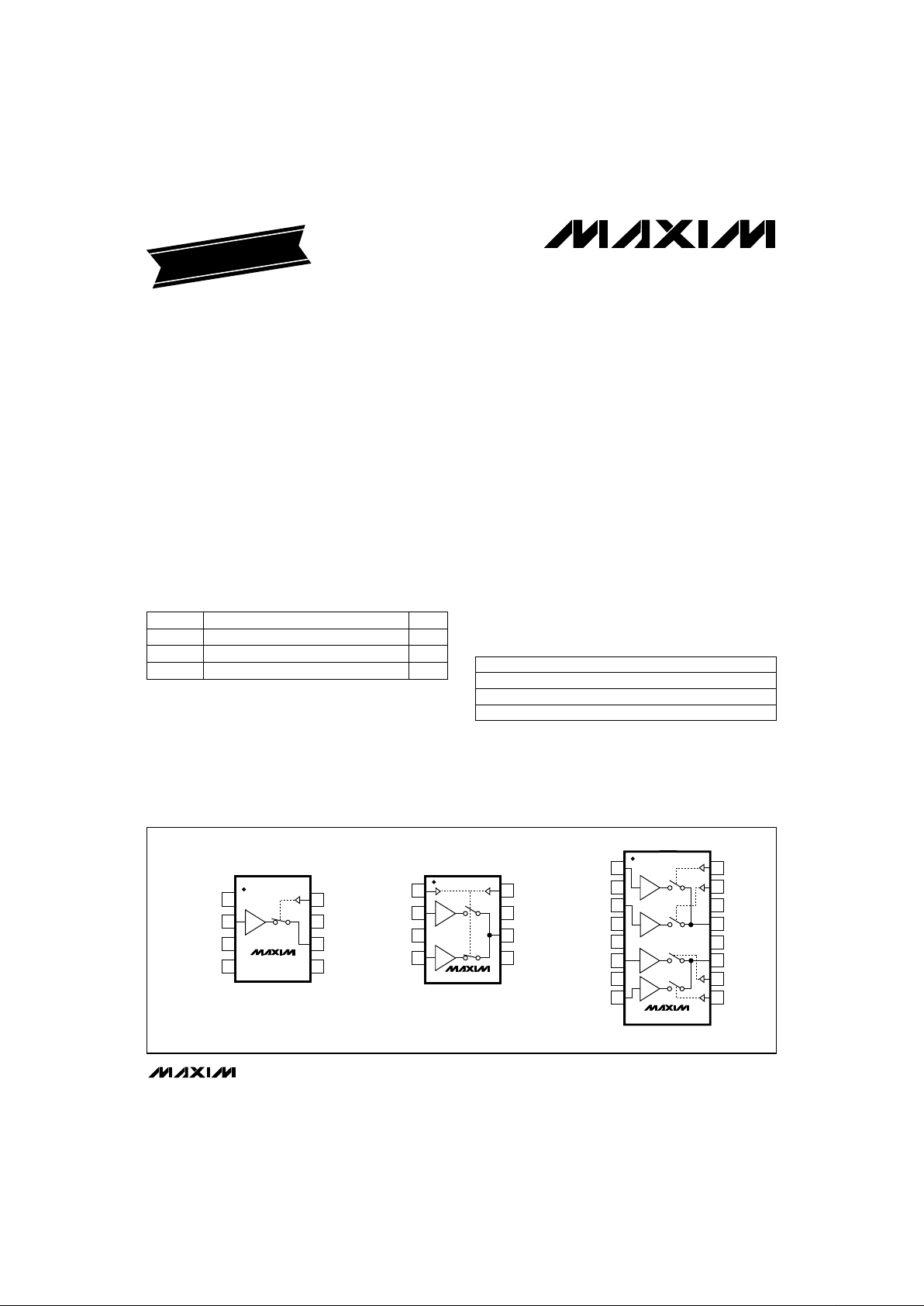
MAX4111
TOP VIEW
SO
16
15
14
13
12
11
10
9
1
2
3
4
5
6
7
8
SEL0
SEL1
V
CC
OUT0
GND
IN1
GND
IN0
MAX4221
V
EE
OUT1
SEL2
SEL3
IN3
GND
IN2
GND
Narrow SO
1
2
3
4
8
7
6
5
EN
V
CC
OUT
V
EE
IN1
GND
IN0
A0
MAX4121
SO
___________________________________Pin Configurations/Functional Diagrams
Call toll free 1-800-998-8800 for free samples or literature.
19-0402; Rev 0; 6/95
PART
MAX4111CSA
MAX4121CSA
MAX4221CSE
0°C to +70°C
0°C to +70°C
0°C to +70°C
TEMP. RANGE PIN-PACKAGE
8 SO
8 SO
16 Narrow SO
EVALUATION KIT
AVAILABLE
______________Ordering Information
PART DESCRIPTION PINS
MAX4111 SPST, single-input, single-output switch 8
MAX4121 SPDT, 2-input, single-output switch 8
MAX4221 Dual, SPDT, 2-input, single-output switch 16
MAX4111/MAX4121/MAX4221
330MHz Buffered Video Switches/
Crosspoint Building Blocks
2 _______________________________________________________________________________________
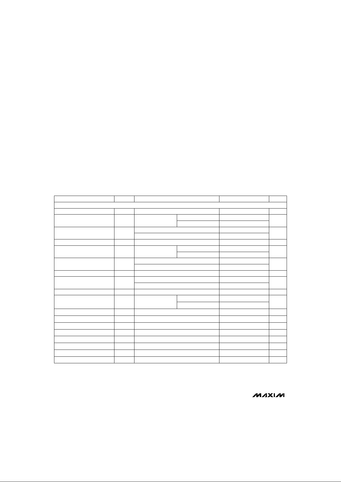
ABSOLUTE MAXIMUM RATINGS
ELECTRICAL CHARACTERISTICS
(VS= ±5V, -2.5V ≤ VIN≤ +2.5V, RL= 5kΩ, CL≤ 5pF, TA= 0°C to +70°C, unless otherwise noted. Typical values are at TA= +25°C.)
Stresses beyond those listed under “Absolute Maximum Ratings” may cause permanent damage to the device. These are stress ratings only, and functional
operation of the device at these or any other conditions beyond those indicated in the operational sections of the specifications is not implied. Exposure to
absolute maximum rating conditions for extended periods may affect device reliability.
Supply Voltages
V
CC
....................................................................................+6V
V
EE
......................................................................................-6V
V
CC-VEE
...........................................................................+12V
Analog Input Voltage .......................(V
EE
- 0.3V) to (VCC+ 0.3V)
Digital Input Voltage...................................-0.3V to (V
CC
+ 0.3V)
Duration of Short Circuit to Ground............................Continuous
Continuous Power Dissipation (T
A
= +70°C)
8-Pin SO (derate 5.88mW/°C above +70°C)................471mW
16-Pin Narrow SO (derate 8.70mW/°C above +70°C) ...696mW
Operating Temperature Range...............................0°C to +70°C
Storage Temperature Range.............................-65°C to +160°C
Junction Temperature......................................................+150°C
Lead Temperature (soldering, 10sec).............................+300°C
VS= ±4.5V to ±5.5V
VS= ±4.5V to ±5.5V
Channel selected
V
OUT
= 0V
f = DC to 50MHz
VIN= ±2.5V
V
VS= ±4.5V to ±5.5V
VS= ±4.5V to ±5.5V
Channel disabled
TA= T
MIN
to T
MAX
Channel selected
VIN= 0V
Per channel
TA= +25°C
VS= ±4.5V to ±5.5V
VIN= 0V, channel enabled or disabled
CONDITIONS
V0.8V
INL
Logic Input Low Voltage
V2.0V
INH
Logic Input High Voltage
pF5C
OUT(OFF)
Disabled Output Capacitance
MΩ30R
OUT(OFF)
Disabled Output Resistance
nA10I
OUT(OFF)
Disabled Output Current
Ω20R
OUT
Output Resistance
V/V
0.97 1.0
A
V
Voltage Gain
0.98 1.0TA= +25°C
dB50PSRRPower-Supply Rejection Ratio
TA= T
MIN
to T
MAX
µA
mV
±15
V
OS
Output Offset Voltage
±5 ±10
10I
INL
pFC
IN
Input Capacitance
4.0 5.5TA= +25°C
TA= T
MIN
to T
MAX
±4.5 ±5.0 ±5.5V
S
3
Operating Supply Voltage
Logic Input Low Current
µA
MΩ
100
R
IN
Input Resistance
0.4
10I
INH
µA
±0.02
I
B
Input Bias Current
6.5
150 200
V±2.5V
IN
Input Voltage Range
±2.5 ±4.0
Channel disabled
Logic Input High Current
UNITSMIN TYP MAXSYMBOLPARAMETER
mAI
CC, IEE
Operating Supply Current
MAX4111/MAX4121
µA
250 350
I
CC, IEE
Disabled Supply Current
DC PARAMETERS
MAX4221
dB
MAX4111/MAX4121/MAX4221
330MHz Buffered Video Switches/
Crosspoint Building Blocks
_______________________________________________________________________________________ 3
ELECTRICAL CHARACTERISTICS
(VS= ±5V, -2.5V ≤ VIN≤ +2.5V, RL= 5kΩ, CL≤ 5pF, TA= 0°C to +70°C, unless otherwise noted. Typical values are at TA= +25°C.)
Note 1: Full-Power Bandwidth is inferred from Slew Rate (SR) testing by the equation SR = ωEP, where EPis the peak output
voltage and ω =2πf.
Note 2: Differential Gain and Phase are tested using a modulated ramp, 100IRE (0.714V).
VIN= 1.4Vp-p
f = 30MHz, VIN= 1.4Vp-p
f = 30MHz, VIN= 1.4Vp-p
V
OUT
= 5Vp-p
Chip-to-chip, f = 3.58MHz
f = 3.58MHz
VIN= 5Vp-p
VIN= 0.1Vp-p
DC to 30MHz
DC to 150MHz
f = 3.58MHz
CONDITIONS
dBc-70Third Harmonic
dBc-65Second Harmonic
degrees±0.2Input-Output Delay Matching
ps860Group Delay
mVp-p13Switching Transient
ns500t
ON
Channel Switching On Time
µs1.0t
OFF
Channel Switching Off Time
-92
degrees0.01DPDifferential Phase (Note 2)
110
700
%0.01DGDifferential Gain (Note 2)
dB0.08Gain Peaking
MHz
45
FPBW
Full-Power Bandwidth
(Note 1)
MHz330f
3dB
-3dB Bandwidth
0.02
dB
0.1
Gain Flatness
UNITSMIN TYP MAXSYMBOLPARAMETER
VIN= 1Vp-p,
f = 30MHz
dB
-70
All-Hostile Crosstalk
VIN= 1Vp-p,
f = 30MHz, see test
circuit
dB
86
Off Isolation
MAX4121
MAX4221
MAX4111
V
OUT
= 1.4Vp-p
V/µs
500
SRSlew Rate
VIN= 0.1Vp-p ps950tr/t
f
Small-Signal Rise Time
MAX4121
84MAX4221
78
AC PARAMETERS
MAX4111/MAX4121/MAX4221
330MHz Buffered Video Switches/
Crosspoint Building Blocks
4 _______________________________________________________________________________________
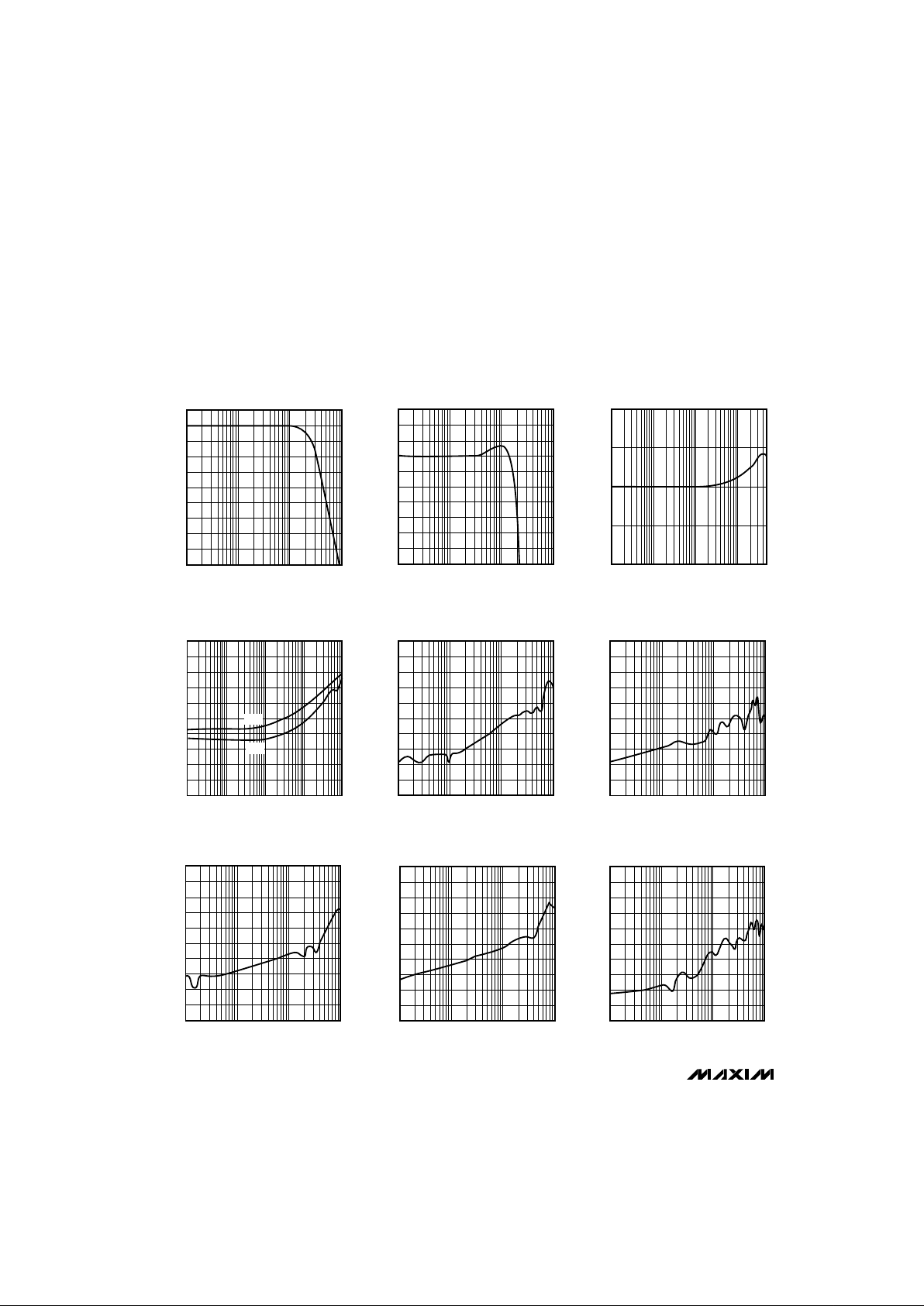
__________________________________________Typical Operating Characteristics
(VS= ±5V, RL= 5kΩ, CL≤ 5pF, TA = +25°C, unless otherwise noted.)
-2
1 10 1000
GAIN vs. FREQUENCY
-10
-6
0
2
-8
-4
-12
-16
-18
-14
MAX4111 TOC-01
FREQUENCY (MHz)
GAIN (dB)
100
-0.1
1 10 100
GAIN FLATNESS
-0.3
0
-0.4
-0.2
-0.6
-0.7
-0.5
0.1
0.2
0.3
MAX4111 TOC-02
FREQUENCY (MHz)
GAIN (dB)
1000
0.1 1 100 500
OUTPUT RESISTANCE vs. FREQUENCY
40
10
0
20
30
MAX4111 TOC-03
FREQUENCY (MHz)
OUTPUT RESISTANCE (Ω)
10
0
10k 100k 10M 100M
POWER-SUPPLY REJECTION RATIO
vs. FREQUENCY
40
20
-10
30
10
50
60
70
80
90
MAX4111 TOC-04
FREQUENCY (Hz)
AMPLITUDE (dB)
1M
V
CC
V
EE
-40
1 100 1000
MAX4111
OFF ISOLATION vs. FREQUENCY
40
0
20
-20
60
140
160
100
120
80
MAX4111 TOC-07
FREQUENCY (MHz)
AMPLITUDE (dB)
10
40
1 100 1000
MAX4121 ALL-HOSTILE CROSSTALK
vs. FREQUENCY
-40
0
-20
20
-60
-140
-160
-100
-120
-80
MAX4111 TOC-05
FREQUENCY (MHz)
AMPLITUDE (dB)
10
40
1 10 1000
MAX4221 ALL-HOSTILE CROSSTALK
vs. FREQUENCY
-40
0
60
-20
20
-60
-140
-100
-120
-80
MAX4111 TOC-06
FREQUENCY (MHz)
AMPLITUDE (dB)
100
-40
1 100 1000
MAX4121
OFF ISOLATION vs. FREQUENCY
40
0
20
-20
60
140
160
100
120
80
MAX4111 TOC-08
FREQUENCY (MHz)
AMPLITUDE (dB)
10
-40
1 10 1000
MAX4221
OFF ISOLATION vs. FREQUENCY
40
0
-60
20
-20
60
140
100
120
80
MAX4111 TOC-09
FREQUENCY (MHz)
AMPLITUDE (dB)
100

MAX4111/MAX4121/MAX4221
330MHz Buffered Video Switches/
Crosspoint Building Blocks
_______________________________________________________________________________________
5
MAX14111 TOC-10
TIME (5ns/div)
VOLTS
(100mV/div)
IN
GND
GND
OUT
SMALL-SIGNAL PULSE RESPONSE
(RL = 5kΩ)
MAX14111 TOC-11
TIME (5ns/div)
OUT
(1V/div)
IN
(2.5V/div)
GND
GND
LARGE-SIGNAL PULSE RESPONSE
(RL = 5kΩ)
VOLTS
MAX14111 TOC-12
TIME (5ns/div)
VOLTS
(100mV/div)
IN
GND
GND
OUT
SMALL-SIGNAL PULSE RESPONSE
(CL = 47pF, RL = open)
MAX14111 TOC-14
TIME (1µs/div)
1V/div
2V/div
ENABLE/DISABLE DELAY TIME
(INPUT = 1.1V)
OUTPUT
ENABLE
OUT
GND
MAX14111 TOC-13
TIME (10ns/div)
OUT
(1V/div)
IN
2.5V/div
GND
GND
LARGE-SIGNAL PULSE RESPONSE
(CL = 47pF, RL = open)
VOLTS
MAX14111 TOC-15
TIME (1µs/div)
10mV/div
2V/div
OUTPUT GLITCH AMPLITUDE
AMPLITUDE
OUTPUT
A0
____________________________Typical Operating Characteristics (continued)
(VS= ±5V, RL= 5kΩ, CL≤ 5pF, TA = +25°C, unless otherwise noted.)

MAX4111/MAX4121/MAX4221
330MHz Buffered Video Switches/
Crosspoint Building Blocks
6 _______________________________________________________________________________________
____________________________Typical Operating Characteristics (continued)
(VS= ±5V, RL= 5kΩ, CL≤ 5pF, TA = +25°C, unless otherwise noted.)
1 100 1M
10G
100M
NOISE VOLTAGE
vs. FREQUENCY
3
100
30
10
1
MAX4111 TOC-16
FREQUENCY (Hz)
NOISE VOLTAGE (nV √
Hz
)
10k
3.4
070
SUPPLY CURRENT
vs. TEMPERATURE
5.0
MAX4111 TOC-17
TEMPERATURE (°C)
SUPPLY CURRENT (mA)
30
4.2
3.8
10 20 60
4.6
3.6
4.4
4.0
4.8
40
50
I
EE
I
CC
-0.110
-3
GAIN vs. INPUT VOLTAGE
AND TEMPERATURE
MAX4111 TOC-18
INPUT VOLTAGE (V)
GAIN (dB)
-0.105
-0.100
-0.095
-0.090
-0.085
-2 -1 0 1 2 3
TA = +25°C
TA = 0°C
TA = +70°C
0
0
BANDWIDTH vs.
LOAD CAPACITANCE
MAX4111 TOC-19
LOAD CAPACITANCE (pF)
BANDWIDTH (MHz)
50
100
150
200
250
300
350
20 40 60 80 100
RL = OPEN
-3dB BW
-0.1dB BW
-1.6
0
GAIN vs.
LOAD RESISTANCE
MAX4111 TOC-20
RL(kΩ)
GAIN (dB)
-1.4
-1.2
-1.0
-0.8
-0.6
-0.4
-0.2
0
12345

MAX4111/MAX4121/MAX4221
330MHz Buffered Video Switches/
Crosspoint Building Blocks
_______________________________________________________________________________________ 7
_______________Detailed Description
The MAX4111/MAX4121/MAX4221 video switches are
manufactured with Maxim’s proprietary, ultra-high frequency, complementary bipolar process that yields
high bandwidth and low capacitance. Make-beforebreak switching is used to reduce noise and glitches,
even when switching from part to part in large arrays.
The input buffers provide a constant high input impedance, and prevent the make-before-break action from
feeding back to the input.
The design of the switching mechanism limits the
inevitable glitch to less than 13mVp-p. In addition, the
glitch pulse is positive to avoid confusion with negative
sync pulses.
Unity-gain buffers isolate other inputs from the switching action of large multiplex arrays. These buffers can
drive 5kΩ resistive loads. In addition, these devices
drive capacitive loads without oscillation. Load capacitance is limited only by system bandwidth requirements.
The MAX4111/MAX4121/MAX4221 do not contain
buffer latches. The digital inputs are transparent.
______________________________________________________________Pin Description
MAX4221
MAX4121
MAX4111
15, 16
11, 13
9, 10
—
14
12
—
6, 8
—
1, 3
—
—
2, 4, 5, 7
PIN
—
—
—
8
7
5
6
—
—
2, 4
—
1
3
Logic Inputs. Channel Selection Bits for OUT0 of the dual 2x1 (MAX4221). See
Table 3.
SEL1,
SEL0
—
Signal Outputs
OUT1,
OUT0
—
Logic Inputs. Channel Selection Bits for OUT1 of the dual 2x1 (MAX4221).
See Table 3.
SEL3,
SEL2
—
Logic Input. Output Enable for the 1x1, 2x1 switches. A logic high on this
pin enables the output. A logic low causes the output to assume a highimpedance state, and reduces supply current.
EN8
Positive Power-Supply Voltage. Connect to +5V. Decouple to power ground.V
CC
7
Negative Power-Supply Voltage. Connect to -5V. Decouple to power ground.V
EE
5
Signal OutputOUT6
Signal Inputs for the dual 2x1 switchIN2, IN3—
Signal InputIN2
Signal InputIN0, IN1—
No Connect—not internally connectedN.C.4
Logic Input. Channel Selection Bit for the 2x1. See Table 2.A0—
Analog (signal) ground. Since inputs are isolated by these grounds, GND
should be as noise-free as possible.
GND1, 3
FUNCTIONNAME

MAX4111/MAX4121/MAX4221
330MHz Buffered Video Switches/
Crosspoint Building Blocks
8 _______________________________________________________________________________________
__________Applications Information
Grounding, Bypassing,
and PC Board Layout
To obtain the full 330MHz bandwidth of these switches,
Microstrip and Stripline techniques are recommended.
To ensure your PC board does not degrade the
switch’s performance, it’s wise to design the board for
a frequency greater than 1GHz. Even with very short
runs, it’s good practice to use this technique at critical
points such as inputs and outputs.
Use the following guidelines when designing the board:
• Do not use wire-wrap boards, because they are too
inductive.
• Do not use IC sockets. They increase parasitic
capacitance and inductance.
• In general, surface-mount components have shorter
leads and lower parasitic reactance, and give better
high-frequency performance than through-hole components.
• The PC board should have at least two layers, with
one side a signal side and the other a ground plane.
• Keep signal lines as short and straight as possible.
Do not make 90° turns; round all corners.
• The ground plane should be as free from voids as
possible.
Bypass Components—Capacitors
Surface-mount ceramic capacitors are recommended
to achieve good high-frequency bypassing. A 0.1µF
capacitor in parallel with a 1000pF capacitor should be
used for each supply. The capacitors should be located as close to the ICs supply pins as possible, with the
smaller value capacitor being closer to the IC than the
other.
Creating Larger Arrays
The MAX4111/MAX4121/MAX4221 were designed as
building blocks for larger arrays. The single-pole switch
allows the system designer much greater control over
crosstalk than multiple switches in a single IC. For this
reason, cable drivers have not been included in the
switch design because of the high-power drive
required (see Figure 6).
Even though the stability of these devices is not worsened by adding capacitance, you may want to limit the
number of switches connected together. The
MAX4111/MAX4121/MAX4221 have a finite input capacitance of about 3pF and a dynamic output resistance
of about 20Ω. This causes a pole at a little more than
2.7GHz. However, in a large array with many switch
inputs, the total capacitance is N x 3pF, where “N” is
the number of switches connected in parallel. The pole
will be located at:
C
STRAY
= Stray capacitance at the interconnect
If the maximum number of switches that may be connected while still maintaining bandwidth is less than
your system requirements, use a unity-gain buffer
amplifier to isolate the switch from the remainder of the
inputs.
1
23 20π ( ) xNx pF C x
MHz
STRAY
+Ω
Table 1. MAX4111 Truth Table
Table 2. MAX4121 Truth Table
Table 3. MAX4221 Truth Table
EN OUT
0 High-Z
1 IN
A0 EN OUT
X 0 High-Z
0 1 IN0
1 1 IN1
Note: SEL0 = SEL1 = 1 and/or SEL2 = SEL3 = 1 is not
allowed. Enabling these states will not damage the device,
but may cause excessive supply currents and distortion.
NA11
IN310
IN201
High-Z00
OUT1SEL3SEL2
NA11
IN110
IN001
High-Z00
OUT0SEL1SEL0

MAX4111/MAX4121/MAX4221
330MHz Buffered Video Switches/
Crosspoint Building Blocks
_______________________________________________________________________________________ 9
_________________________________________________________________Test Circuits
MAX4111
NETWORK
ANALYZER
* 20Ω RESISTOR USED TO SIMULATE THE OUTPUT OF AN ON SWITCH.
IN THIS WAY, OPERATION IN AN ARRAY IS SIMULATED.
50Ω 20Ω∗
MAX4121
HIGH-IMPEDANCE
PROBE
NETWORK
ANALYZER
MAX4121
HIGH-IMPEDANCE
PROBE
NETWORK
ANALYZER
* 20Ω RESISTOR USED TO SIMULATE THE OUTPUT OF AN ON SWITCH.
IN THIS WAY, OPERATION IN AN ARRAY IS SIMULATED.
20Ω∗
Figure 1. MAX4111 Off Isolation
Figure 2. MAX4121 All-Hostile Crosstalk
Figure 3. MAX4121 Off Isolation

MAX4111/MAX4121/MAX4221
330MHz Buffered Video Switches/
Crosspoint Building Blocks
10 ______________________________________________________________________________________
MAX4221
NETWORK
ANALYZER
HIGH-IMPEDANCE
PROBE
50Ω
50Ω
50Ω
50Ω
MAX4221
NETWORK
ANALYZER
* 20Ω RESISTOR USED TO SIMULATE THE OUTPUT OF AN ON SWITCH.
IN THIS WAY, OPERATION IN AN ARRAY IS SIMULATED.
20Ω∗
50Ω
50Ω
50Ω
50Ω
HIGH-IMPEDANCE
PROBE
Figure 5. MAX4221 Off IsolationFigure 4. MAX4221 All-Hostile Crosstalk

MAX4111/MAX4121/MAX4221
330MHz Buffered Video Switches/
Crosspoint Building Blocks
______________________________________________________________________________________ 11
16
15
14
13
12
11
10
9
1
2
3
4
5
6
7
8
SEL0A
SEL1A
V
CC
OUTA
MAX4221
V
EE
OUTB
SEL0B
SEL1B
IN0A
75Ω
75Ω
75Ω
75Ω
IN1A
IN0B
IN1B
16
15
14
13
12
11
10
9
1
2
3
4
5
6
7
8
SEL2A
SEL3A
V
CC
MAX4221
V
EE
SEL2B
SEL3B
IN2A
75Ω
75Ω
75Ω
75Ω
IN3A
IN2B
IN3B
16
15
14
13
12
11
10
9
1
2
3
4
5
6
7
8
SEL4A
SEL5A
V
CC
MAX4221
V
EE
SEL4B
SEL5B
IN4A
75Ω
75Ω
75Ω
75Ω
IN5A
IN4B
IN5B
16
15
14
13
12
11
10
9
1
2
3
4
5
6
7
8
SEL6A
= SIGNAL GROUND
POWER- SUPPLY BYPASSING NOT SHOWN.
SEL7A
V
CC
MAX4221
V
EE
SEL6B
SEL7B
IN6A
75Ω
75Ω
75Ω
75Ω
IN7A
IN6B
IN7B
Figure 6. 8x2 Multiplexer Using MAX4221

Maxim cannot assume responsibility for use of any circuitry other than circuitry entirely embodied in a Maxim product. No circuit patent licenses are
implied. Maxim reserves the right to change the circuitry and specifications without notice at any time.
12
__________________Maxim Integrated Products, 120 San Gabriel Drive, Sunnyvale, CA 94086 (408) 737-7600
© 1995 Maxim Integrated Products Printed USA is a registered trademark of Maxim Integrated Products.
MAX4111/MAX4121/MAX4221
330MHz Buffered Video Switches/
Crosspoint Building Blocks
________________________________________________________Package Information
DIM
A
A1
B
C
E
e
H
L
MIN
0.053
0.004
0.014
0.007
0.150
0.228
0.016
MAX
0.069
0.010
0.019
0.010
0.157
0.244
0.050
MIN
1.35
0.10
0.35
0.19
3.80
5.80
0.40
MAX
1.75
0.25
0.49
0.25
4.00
6.20
1.27
INCHES MILLIMETERS
21-0041A
Narrow SO
SMALL-OUTLINE
PACKAGE
(0.150 in.)
DIM
D
D
D
MIN
0.189
0.337
0.386
MAX
0.197
0.344
0.394
MIN
4.80
8.55
9.80
MAX
5.00
8.75
10.00
INCHES MILLIMETERS
PINS
8
14
16
1.270.050
L
0°-8°
HE
D
e
A
A1
C
0.101mm
0.004in.
B
 Loading...