Maxim MAX4218ESD, MAX4216ESA, MAX4213EUA, MAX4213ESA, MAX4212EUK Datasheet
...
General Description
The MAX4212/MAX4213 single, MAX4216 dual,
MAX4218 triple, and MAX4220 quad op amps are
unity-gain-stable devices that combine high-speed performance with rail-to-rail outputs. The MAX4213/
MAX4218 have a disable feature that reduces powersupply current to 400µA and places the outputs into a
high-impedance state. These devices operate from a
+3.3V to +10V single supply or from ±1.65V to ±5V
dual supplies. The common-mode input voltage range
extends beyond the negative power-supply rail (ground
in single-supply applications).
These devices require only 5.5mA of quiescent supply
current while achieving a 300MHz -3dB bandwidth and
a 600V/µs slew rate. Input voltage noise is only
10nV/√Hz and input current noise is only 1.3pA/√Hz for
either the inverting or noninverting input. These parts
are an excellent solution in low-power/low-voltage systems that require wide bandwidth, such as video, communications, and instrumentation. In addition, when
disabled, their high output impedance makes them
ideal for multiplexing applications.
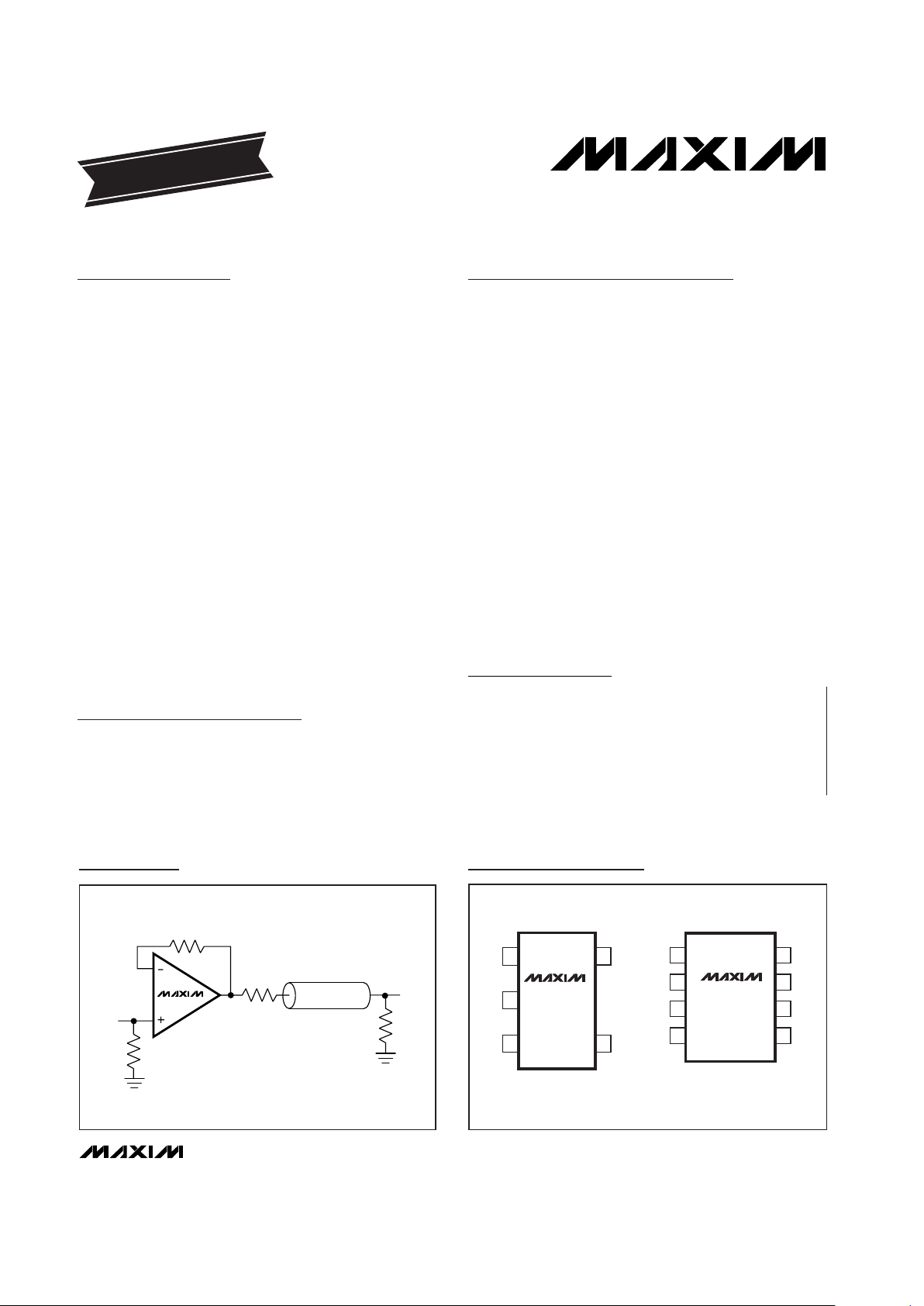
The MAX4212 comes in a miniature 5-pin SOT23 package, while the MAX4213/MAX4216 come in 8-pin µMAX
and SO packages. The MAX4218/MAX4220 are available in a space-saving 16-pin QSOP, as well as a
14-pin SO.
Applications
Battery-Powered Instruments
Video Line Driver
Analog-to-Digital Converter Interface
CCD Imaging Systems
Video Routing and Switching Systems
Features
♦ High Speed:
300MHz -3dB Bandwidth (MAX4212/13)
200MHz -3dB Bandwidth (MAX4216/18/20)
50MHz 0.1dB Gain Flatness (MAX4212/13)
600V/µs Slew Rate
♦ Single 3.3V/5.0V Operation
♦ Rail-to-Rail Outputs
♦ Input Common-Mode Range Extends Beyond V
EE
♦ Low Differential Gain/Phase: 0.02%/0.02°
♦ Low Distortion at 5MHz:
-78dBc SFDR
-75dB Total Harmonic Distortion
♦ High Output Drive: ±100mA
♦ 400µA Shutdown Capability (MAX4213/18)
♦ High Output Impedance in Off State (MAX4213/18)
♦ Space-Saving SOT23-5, µMAX, or QSOP Packages
MAX4212/MAX4213/MAX4216/MAX4218/MAX4220
Miniature, 300MHz, Single-Supply,
Rail-to-Rail Op Amps with Enable
________________________________________________________________
Maxim Integrated Products
1
V
EE
IN-
IN+
1
5
V
CC
OUT
MAX4212
SOT23-5
TOP VIEW
2
3
4
OUT
N.C.
V
EE
1
2
8
7
EN
V
CC
IN-
IN+
N.C.
µMAX/SO
3
4
6
5
MAX4213
Pin Configuration
R
O
50Ω
IN
V
OUT
ZO = 50Ω
UNITY-GAIN LINE DRIVER
(R
L
= RO + RTO)
R
F
24Ω
R
TO
50Ω
R
TIN
50Ω
MAX4212
Typical Operating Circuit
19-1178; Rev 1; 6/98
EVALUATION KIT MANUAL
FOLLOWS DATA SHEET
Ordering Information
Ordering Information continued at end of data sheet.
Pin Configurations continued at end of data sheet.
For free samples & the latest literature: http://www.maxim-ic.com, or phone 1-800-998-8800.
For small orders, phone 1-800-835-8769.
—-40°C to +85°C
MAX4213ESA
8 SO
—
ABAF
SOT
TOP
MARK
-40°C to +85°CMAX4213EUA
-40°C to +85°C
MAX4212EUK
8 µMAX
5 SOT23-5
PIN-
PACKAGE
TEMP.
RANGE
PART
MAX4212/MAX4213/MAX4216/MAX4218/MAX4220
Miniature, 300MHz, Single-Supply,
Rail-to-Rail Op Amps with Enable
2 _______________________________________________________________________________________
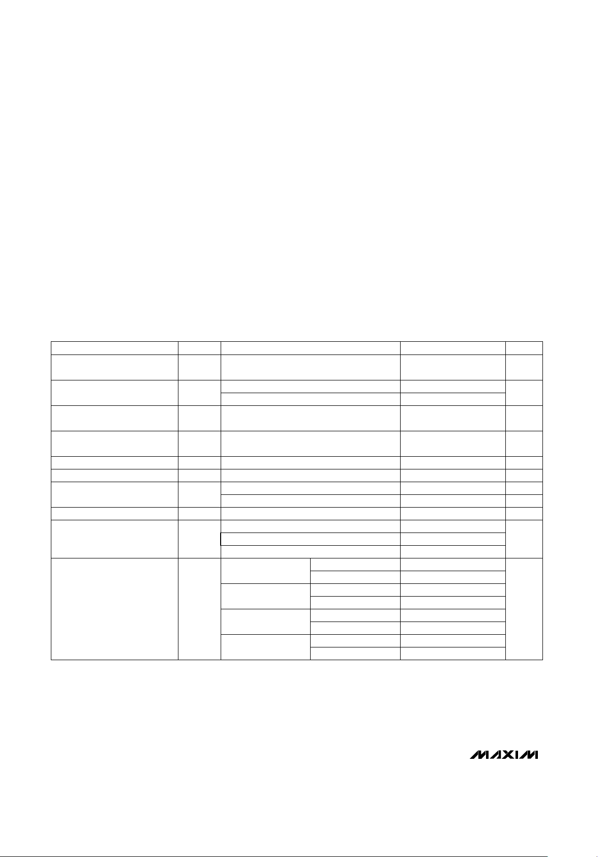
ABSOLUTE MAXIMUM RATINGS
DC ELECTRICAL CHARACTERISTICS
(VCC= +5V, VEE= 0V, EN_ = +5V, RL= 2kΩ to VCC/ 2, V
OUT
= VCC/ 2, TA= T
MIN
to T
MAX
, unless otherwise noted. Typical values
are at T
A
= +25°C.)
Supply Voltage (V
CC
to VEE)................................................+12V
IN_-, IN_+, OUT_, EN_.....................(V
EE
- 0.3V) to (VCC+ 0.3V)
Output Short-Circuit Duration to V
CC
or VEE............. Continuous
Continuous Power Dissipation (T
A
= +70°C)
5-Pin SOT23 (derate 7.1mW/°C above +70°C)...........571mW
8-Pin SO (derate 5.9mW/°C above +70°C).................471mW
8-Pin µMAX (derate 4.5mW/°C above +70°C) ............221mW
14-Pin SO (derate 8.3mW/°C above +70°C)...............667mW
16-Pin QSOP (derate 8.3mW/°C above +70°C)..........667mW
Operating Temperature Range ...........................-40°C to +85°C
Storage Temperature Range.............................-65°C to +150°C
Lead Temperature (soldering, 10sec).............................+300°C
Stresses beyond those listed under “Absolute Maximum Ratings” may cause permanent damage to the device. These are stress ratings only, and functional
operation of the device at these or at any other conditions beyond those indicated in the operational sections of the specifications is not implied. Exposure
to absolute maximum rating conditions for extended periods may affect device reliability.
VOL- V
EE
VCC- V
OH
VOL- V
EE
VCC- V
OH
VOL- V
EE
VCC- V
OH
VOL- V
EE
VCC- V
OH
0.60
0.70
RL= 50Ω
0.30 0.50
0.30 0.50
RL= 150Ω
0.06 0.20
0.06 0.20
RL= 2kΩ
0.05
Output Voltage Swing V
OUT
V
0.05
RL= 10kΩ
57
1.0V ≤ V
OUT
≤ 4V, RL= 50Ω
52 59
0.5V ≤ V
OUT
≤ 4.5V, RL= 150Ω
55 61
0.25V ≤ V
OUT
≤ 4.75V, RL= 2kΩ
3
MΩ
Common mode (-0.2V ≤ VCM≤ +2.75V)
49MAX42_ _ES_, MAX42_ _EEE
PARAMETER SYMBOL MIN TYP MAX UNITS
Input Resistance R
IN
70
kΩ
Input Offset Current I
OS
0.1 1.0 µA
Input Bias Current I
B
5.4 9.0 µA
Input Offset Voltage Matching ±1 mV
Common-Mode Rejection Ratio CMRR 70 100 dB
Open-Loop Gain (Note 1) A
VOL
dB
Input Offset Voltage (Note 1)
Input Common-Mode
Voltage Range
V
CM
VEE-V
CC
-
0.20 2.25
V
V
OS
412
mV
Input Offset Voltage
Temperature Coefficient
TC
VOS
8 µV/°C
CONDITIONS
Differential mode (-1V ≤ VIN≤ +1V)
(Note 1)
(Note 1)
Any channels for MAX4216/MAX4218/
MAX4220
(V
EE
- 0.2V) ≤ V
CM
≤ (V
CC
- 2.25V)
Guaranteed by CMRR test
MAX4212EUK, MAX421_EUA
MAX4212/MAX4213/MAX4216/MAX4218/MAX4220
Miniature, 300MHz, Single-Supply,
Rail-to-Rail Op Amps with Enable
_______________________________________________________________________________________ 3
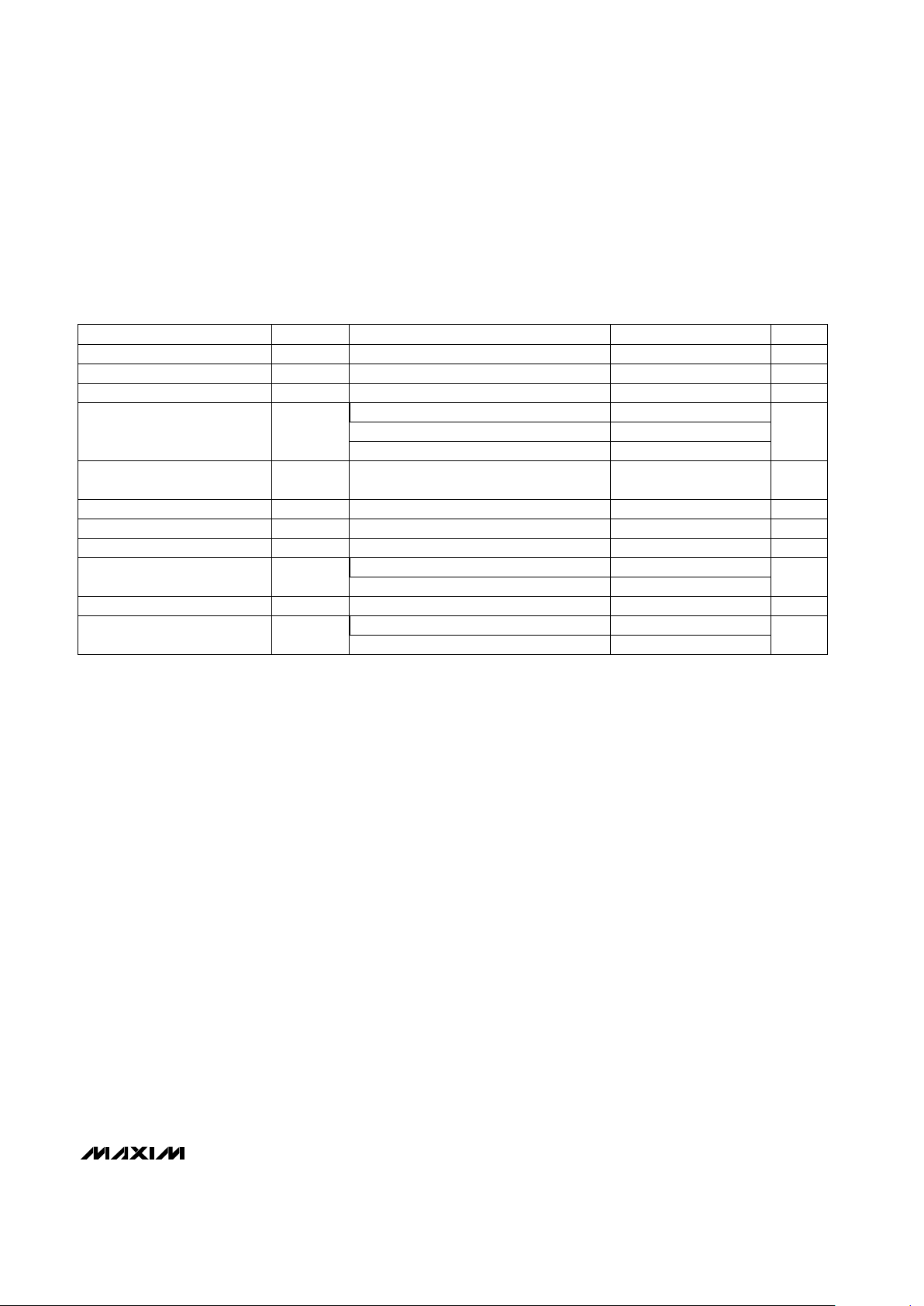
DC ELECTRICAL CHARACTERISTICS (continued)
(VCC= +5V, VEE= 0V, EN_ = +5V, RL= 2kΩ to VCC/ 2, V
OUT
= VCC/ 2, TA= T
MIN
to T
MAX
, unless otherwise noted. Typical values
are at T
A
= +25°C.)
EN_ = 0V
EN_ Logic Input Low Current I
IL
200 300
µA
(VEE+ 0.2V) ≤ EN_ ≤ V
CC
Output Current I
OUT
±100 ±120 mA
RL= 20Ω to VCCor V
EE
0.40 0.55Disabled (EN_ = 0V)
Quiescent Supply Current
(per Amplifier)
I
S
5.5 7.0
mA
Enabled
EN_ Logic Input High Current I
IH
0.5 10 µAEN_ = 5V
0.5
EN_ Logic-High Threshold V
IH
V
CC
- 1.6 V
EN_ Logic-Low Threshold V
IL
VCC- 2.6 V
Disabled Output Resistance R
OUT (OFF)
20 35
kΩ
EN_ = 0V, 0V ≤ V
OUT
≤ 5V (Note 3)
45VCC= 3.3V, VEE= 0V, VCM= +0.90V
PARAMETER SYMBOL MIN TYP MAX UNITS
Operating Supply-Voltage
Range
V
S
3.15 11.0 V
60 66
Power-Supply Rejection Ratio
(Note 2)
PSRR
52 57
dB
Output Short-Circuit Current I
SC
±150 mA
Open-Loop Output Resistance R
OUT
8
Ω
CONDITIONS
VCCto V
EE
VCC= 5V, VEE= -5V, VCM= 0V
VCC= 5V, VEE= 0V, VCM= +2.0V
Sinking or sourcing
MAX4212/MAX4213/MAX4216/MAX4218/MAX4220
Miniature, 300MHz, Single-Supply,
Rail-to-Rail Op Amps with Enable
4 _______________________________________________________________________________________
Note 1: Tested with VCM= +2.5V.
Note 2: PSR for single +5V supply tested with V
EE
= 0V, VCC= +4.5V to +5.5V; for dual ±5V supply with VEE= -4.5V to -5.5V,
V
CC
= +4.5V to +5.5V; and for single +3.3V supply with VEE= 0V, VCC= +3.15V to +3.45V.
Note 3: Does not include the external feedback network’s impedance.
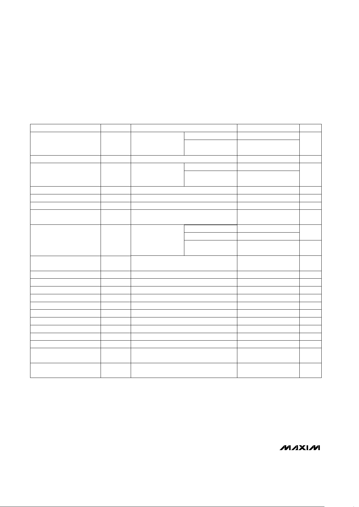
AC ELECTRICAL CHARACTERISTICS
(VCC= +5V, VEE= 0V, VCM= 2.5V, EN_ = +5V, RF= 24Ω, RL= 100Ω to VCC/ 2, V
OUT
= VCC/ 2, A
VCL
= +1, TA= +25°C, unless
otherwise noted.)
MAX4216/MAX4218/MAX4220,
f = 10MHz, V
OU
T
= 2Vp-p
dB-95X
TALK
Amplifier Crosstalk
MAX4216/MAX4218/MAX4220,
f = 10MHz, V
OUT
= 20mVp-p
dB0.1Amplifier Gain Matching
µs1t
OFF
Amplifier Disable Time
fC= 5MHz, V
OUT
= 2Vp-p dBc-78SFDR
Spurious-Free Dynamic
Range
Total harmonic
distortion
3rd harmonic
2nd harmonic
MAX4216/MAX4218/
MAX4220
MAX4212/MAX4213
MAX4216/MAX4218/
MAX4220
MAX4212/MAX4213
f = 10MHz
EN_ = 0V
f = 10kHz
f = 10kHz
V
OUT
= 20mVp-p
NTSC, RL= 150Ω
NTSC, RL= 150Ω
fC= 10MHz, A
VCL
= +2
fC= 5MHz,
V
OUT
= 2Vp-p
V
OUT
= 100mVp-p
f1 = 10.0MHz, f2 = 10.1MHz, V
OUT
= 1Vp-p
V
OUT
= 2V step
V
OUT
= 2V step
V
OUT
= 2Vp-p
V
OUT
= 20mVp-p
CONDITIONS
ns100t
ON
Amplifier Enable Time
Ω
6Z
OUT
Output Impedance
pF2C
OUT (OFF)
Disabled Output Capacitance
pF1C
IN
Input Capacitance
pA/√Hz
1.3i
n
Input Noise-Current Density
nV/√Hz
10e
n
Input Noise-Voltage Density
%0.02DGDifferential Gain Error
degrees0.02DPDifferential Phase Error
dBm11Input 1dB Compression Point
dBc35IP3
Two-Tone, Third-Order
Intermodulation Distortion
dB-75
-82
HDHarmonic Distortion
200
MHz
300
BW
SS
Small-Signal -3dB Bandwidth
dBc
-78
ns1tR, t
F
Rise/Fall Time
ns45t
S
Settling Time to 0.1%
V/µs600SRSlew Rate
MHz180BW
LS
Large-Signal -3dB Bandwidth
MHz
50
BW
0.1dB
Bandwidth for 0.1dB Gain
Flatness
35
UNITSMIN TYP MAXSYMBOLPARAMETER
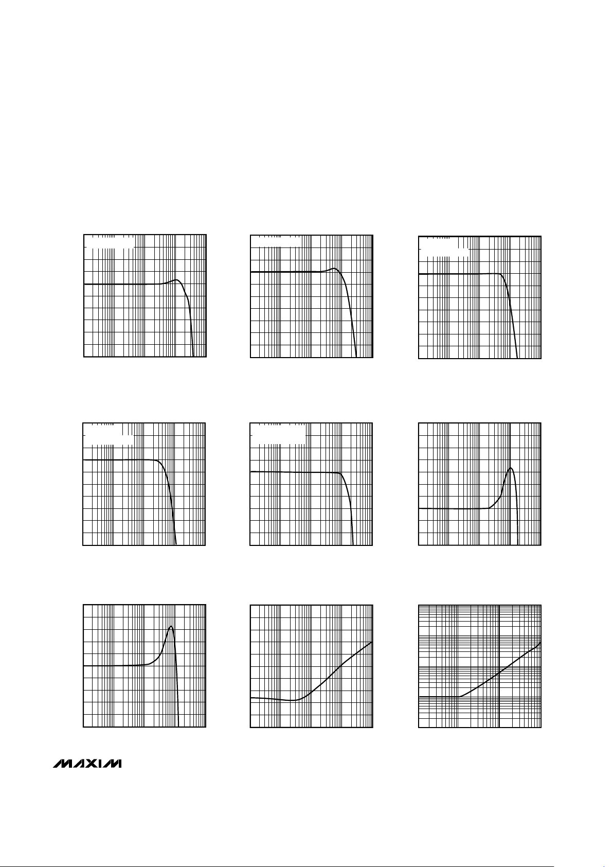
MAX4212/MAX4213/MAX4216/MAX4218/MAX4220
Miniature, 300MHz, Single-Supply,
Rail-to-Rail Op Amps with Enable
_______________________________________________________________________________________
5
4
-6
100k 1M 10M 100M 1G
MAX4212/13
SMALL-SIGNAL GAIN vs. FREQUENCY
-4
MAX4212/3/6/8/20-01
FREQUENCY (Hz)
GAIN (dB)
-2
0
2
3
-5
-3
-1
1
V
OUT
= 20mVp-p
3
-7
100k 1M 10M 100M 1G
MAX4216/18/20
SMALL-SIGNAL GAIN vs. FREQUENCY
-5
MAX4212/3/6/8/20-02
FREQUENCY (Hz)
GAIN (dB)
-3
-1
1
2
-6
-4
-2
0
V
OUT
= 20mVp-p
9
-1
100k 1M 10M 100M 1G
MAX4212/13
SMALL-SIGNAL GAIN vs. FREQUENCY
1
MAX4212/3/6/8/20-03
FREQUENCY (Hz)
GAIN (dB)
3
5
7
8
0
2
4
6
A
VCL
= +2
V
OUT
= 20mVp-p
9
-1
100k 1M 10M 100M 1G
MAX4216/18/20
SMALL-SIGNAL GAIN vs. FREQUENCY
1
MAX4212/3/6/8/20-04
FREQUENCY (Hz)
GAIN (dB)
3
5
7
8
0
2
4
6
A
VCL
= +2
V
OUT
= 20mVp-p
0.5
-0.5
0.1M 1M 10M 100M 1G
MAX4216/18/20
GAIN FLATNESS vs. FREQUENCY
-0.3
MAX4212/3/6/8/20-07
FREQUENCY (Hz)
GAIN (dB)
-0.1
0.1
0.3
0.4
-0.4
-0.2
0
0.2
4
-6
100k 1M 10M 100M 1G
LARGE-SIGNAL GAIN vs. FREQUENCY
-4
MAX4212/3/6/8/20-05
FREQUENCY (Hz)
GAIN (dB)
-2
0
2
3
-5
-3
-1
1
V
OUT
= 2Vp-p
V
OUT BIAS
= 1.75V
0.7
-0.3
0.1M 1M 10M 100M 1G
MAX4212/13
GAIN FLATNESS vs. FREQUENCY
-0.1
MAX4212/3/6/8/20-06
FREQUENCY (Hz)
GAIN (dB)
0.1
0.3
0.5
0.6
-0.2
0
0.2
0.4
50
-150
100k 1M 10M 100M 1G
MAX4216/18/20
CROSSTALK vs. FREQUENCY
-110
MAX4212/3/6/8/20-08
FREQUENCY (Hz)
CROSSTALK (dB)
-70
-30
10
30
-130
-90
-50
-10
1000
0.1
0.1M 1M 10M 100M
CLOSED-LOOP OUTPUT IMPEDANCE
vs. FREQUENCY
MAX4212/3/6/8/20-09
FREQUENCY (Hz)
IMPEDANCE (Ω)
100
1
10
__________________________________________Typical Operating Characteristics
(VCC= +5V, VEE= 0V, A
VCL
= +1, RF= 24Ω, RL= 100Ω to VCC/ 2, TA = +25°C, unless otherwise noted.)
 Loading...