MAXIM MAX4214, MAX4215, MAX4217, MAX4219, MAX4222 Technical data
For pricing, delivery, and ordering information, please contact Maxim/Dallas Direct! at
1-888-629-4642, or visit Maxim’s website at www.maxim-ic.com.
_________________General Description
The MAX4214/MAX4215/MAX4217/MAX4219/MAX4222
are precision, closed-loop, gain of +2 (or -1) buffers
featuring high slew rates, high output current drive, and
low differential gain and phase error. They operate with
a single 3.15V to 11V supply or with ±1.575V to ±5.5V
dual supplies. The input common-mode voltage range
extends 100mV beyond the negative power-supply rail,
and the output swings Rail-to-Rail®.
These devices require only 5.5mA of quiescent supply
current while achieving a 230MHz -3dB bandwidth and
a 600V/µs slew rate. In addition, the MAX4215/
MAX4219 have a disable feature that reduces the supply current to 400µA per buffer. Input voltage noise is
only 10nV/√Hz, and input current noise is only
1.3pA/√Hz. This buffer family is ideal for low-power/lowvoltage applications requiring wide bandwidth, such as
video, communications, and instrumentation systems.
For space-sensitive applications, the MAX4214 comes
in a miniature 5-pin SOT23 package.
________________________Applications
Battery-Powered Instruments
Video Line Drivers
Analog-to-Digital Converter Interface
CCD Imaging Systems
Video Routing and Switching Systems
Video Multiplexing Applications
____________________________Features
♦ Internal Precision Resistors for Closed-Loop
Gains of +2V/V or -1V/V
♦ High Speed
230MHz -3dB Bandwidth
90MHz 0.1dB Gain Flatness
(MAX4219/MAX4222)
600V/µs Slew Rate
♦ Single 3.3V/5.0V Operation
♦ Outputs Swing Rail-to-Rail
♦ Input Common-Mode Range Extends Beyond V
EE
♦ Low Differential Gain/Phase Error: 0.03%/0.04°
♦ Low Distortion at 5MHz
-72dBc SFDR
-71dB Total Harmonic Distortion
♦ High Output Drive: ±120mA
♦ Low 5.5mA Supply Current
♦ 400µA Shutdown Supply Current
(MAX4215/MAX4219)
♦ Space-Saving SOT23, µMAX, or QSOP Packages
MAX4214/MAX4215/MAX4217/MAX4219/MAX4222
High-Speed, Single-Supply, Gain of 2,
Closed-Loop, Rail-to-Rail Buffers with Enable
________________________________________________________________ Maxim Integrated Products 1
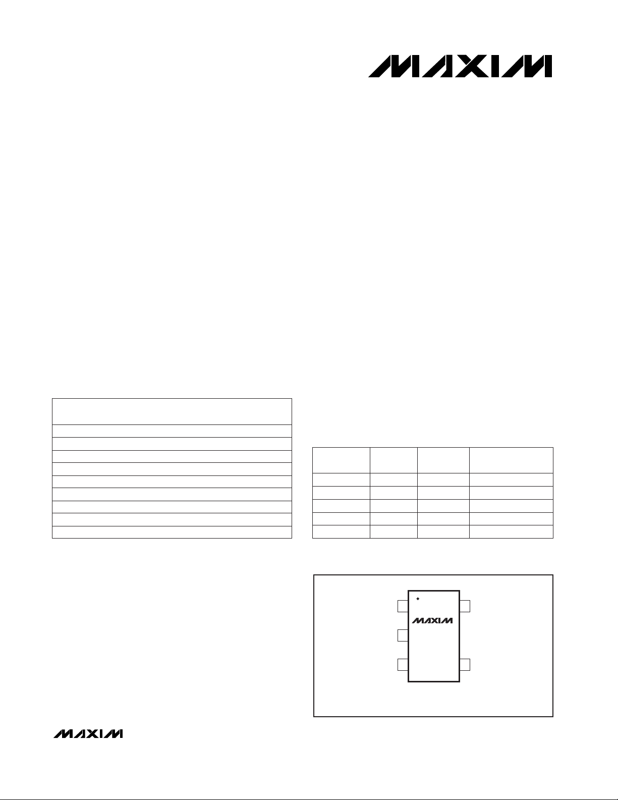
V
EE
IN-
IN+
1
5
V
CC
OUT
MAX4214
SOT23-5
TOP VIEW
2
3
4
19-4754; Rev 1; 8/01
PART
MAX4214EUK-T
MAX4215ESA
MAX4215EUA -40°C to +85°C
-40°C to +85°C
-40°C to +85°C
TEMP RANGE
PINPACKAGE
5 SOT23-5
8 SO
8 µMAX
Typical Application Circuit appears at end of data sheet.
Rail-to-Rail is a registered trademark of Nippon Motorola, Ltd.
Pin Configurations continued at end of data sheet.
NO. OF
AMPS
ENABLE
MAX4214 1 No
MAX4215 1 Yes
PART PIN-PACKAGE
5 SOT23
8 SO/µMAX
MAX4217 2 No
MAX4219 3 Yes
8 SO/µMAX
14 SO, 16 QSOP
MAX4222 4 No 14 SO, 16 QSOP
TOP
MARK
ABAH
—
—
__________________Pin Configurations
_______________Ordering Information
______________________Selector Guide
MAX4217ESA
MAX4217EUA -40°C to +85°C
-40°C to +85°C 8 SO
8 µMAX
—
—
MAX4219ESD
MAX4219EEE -40°C to +85°C
-40°C to +85°C 14 SO
16 QSOP
—
—
MAX4222ESD
MAX4222EEE -40°C to +85°C
-40°C to +85°C 14 SO
16 QSOP
—
—
MAX4214/MAX4215/MAX4217/MAX4219/MAX4222
High-Speed, Single-Supply, Gain of 2,
Closed-Loop, Rail-to-Rail Buffers with Enable
2 _______________________________________________________________________________________
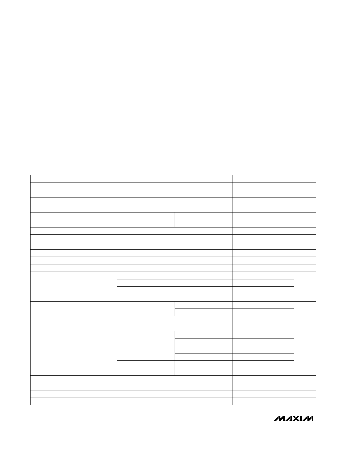
ABSOLUTE MAXIMUM RATINGS
DC ELECTRICAL CHARACTERISTICS
(VCC= 5V, VEE= 0, IN_- = 0, EN_ = 5V, RL= ∞ to 0, V
OUT
= VCC/2, noninverting configuration, TA= T
MIN
to T
MAX
, unless
otherwise noted. Typical values are at T
A
= +25°C.) (Note 1)
Stresses beyond those listed under “Absolute Maximum Ratings” may cause permanent damage to the device. These are stress ratings only, and functional
operation of the device at these or any other conditions beyond those indicated in the operational sections of the specifications is not implied. Exposure to
absolute maximum rating conditions for extended periods may affect device reliability.
Supply Voltage (VCCto VEE)..................................................12V
IN_-, IN_+, OUT_, EN_ ....................(V
EE
- 0.3V) to (VCC+ 0.3V)
Output Short-Circuit Duration to V
CC
or VEE..............Continuous
Continuous Power Dissipation (T
A
= +70°C)
5-Pin SOT23 (derate 7.1mW/°C above +70°C).............571mW
8-Pin SO (derate 5.9mW/°C above +70°C)...................471mW
8-Pin µMAX (derate 4.1mW/°C above +70°C) .............330mW
14-Pin SO (derate 8.3mW/°C above +70°C)................667mW
16-Pin QSOP (derate 8.3mW/°C above +70°C)...........667mW
Operating Temperature Range ...........................-40°C to +85°C
Storage Temperature Range .............................-65°C to +150°C
Lead Temperature (soldering, 10s) .................................+300°C
VCCto VEE, guaranteed by PSRR tests
RL= 50Ω
3.15 11.0
±150
0.04 0.075
IN_-
SOT23-5, µMAX
VEE- 0.1 VCC+ 0.1
SO, QSOP
VCC- V
OH
IN_+
V
VEE- 0.1 VCC- 2.25
Operating Supply Voltage
Range
Sinking or sourcing
VOL- V
EE
VCC- V
OH
VOL- V
EE
VCC- V
OH
IN_+, over input voltage range MΩ3
CONDITIONS
Between any two channels for
MAX4217/MAX4219/MAX4222
410
Input Resistance
IN_+ µA5.4 12I
B
Input Bias Current
mV1
Input Offset Voltage
Matching
V
IN
55 58
Input Voltage Range
µV/°C
45
RL≥ 50Ω, (VEE+ 0.5V) ≤ V
OUT
≤ (VCC- 2.0V)
VCC= 5V, VEE= 0, V
OUT
= 2.0V
60 66
VOL- V
EE
RL= 150Ω
0.04 0.075
RL= 2kΩ
0.06
VCC= 3.3V, VEE= 0, V
OUT
= 0.90V
V
0.06
25
Power-Supply
Rejection Ratio
(Note 2)
V/V1.9 2 2.1
R
IN
MAX4215/MAX4219 VVCC- 2.6V
IL
EN_ Logic Low Threshold
A
V
Voltage Gain
8TCV
OS
Input Offset Voltage Drift
VCC- 1.6
MAX4215/MAX4219, EN_ = 0, 0 ≤ V
OUT
≤ 5V
mV
415
V
OS
Input Offset Voltage
VCC= 5V, VEE= -5V, V
OUT
= 0
f = DCR
OUT
PSRR
Output Resistance
MAX4215/MAX4219
mΩ
VV
IH
EN_ Logic High Threshold
dB
kΩ1
R
OUT(OFF)
Disabled Output
Resistance
UNITSMIN TYP MAXSYMBOLPARAMETER
1.60 1.90
RL= 50Ω
mA
0.75 1.00
I
SC
Short-Circuit Output
Current
±70 ±120
V
OUT
Output Voltage Swing V
RL= 20Ω to VCCor V
EE
mA
±60
I
OUT
Output Current
TA= +25°C
TA= T
MIN
to T
MAX
MAX4214/MAX4215/MAX4217/MAX4219/MAX4222
High-Speed, Single-Supply, Gain of 2,
Closed-Loop, Rail-to-Rail Buffers with Enable
_______________________________________________________________________________________ 3
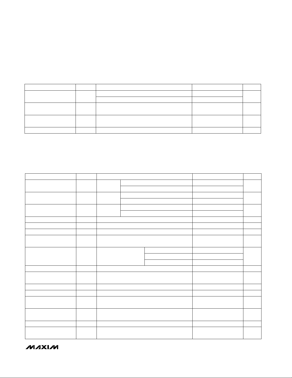
DC ELECTRICAL CHARACTERISTICS (continued)
(VCC= 5V, VEE= 0, IN_- = 0, EN_ = 5V, RL= ∞ to 0, V
OUT
= VCC/2, noninverting configuration, TA= T
MIN
to T
MAX
, unless
otherwise noted. Typical values are at T
A
= +25°C.) (Note 1)
AC ELECTRICAL CHARACTERISTICS
(VCC= 5V, VEE= 0, IN_- = 0, EN_ = 5V, RL= 100Ω to VCC/2, noninverting configuration, TA= T
MIN
to T
MAX
, unless otherwise noted.
Typical values are at T
A
= +25°C.)
CONDITIONS
mA5.5 7.0I
CC
Quiescent Supply
Current (per Buffer)
200 350MAX4215/MAX4219, EN_ = V
EE
0.5 10
0.5
UNITSMIN TYP MAXSYMBOLPARAMETER
µA
µA
MAX4215/MAX4219, EN_ = V
CC
MAX4215/MAX4219, (VEE+ 0.2V) ≤ EN_ ≤ V
CC
I
IH
I
IL
EN_ Logic Input High
Current
EN_ Logic Input Low
Current
MAX4214/MAX4215/MAX4217
230
0.04
10
V
OUT
=
2V
P-P
MHz
220
f = 10MHz
FPBW
Full-Power -3dB
Bandwidth
MAX4214/MAX4215/MAX4217
200
NTSC, RL= 150Ω
MAX4214/MAX4215/MAX4217
MAX4219/MAX4222
MAX4219/MAX4222
MAX4219/MAX4222
V
OUT
= 100mV
P-P
ns1
CONDITIONS
V
OUT
= 2V step
200
Rise/Fall Time
V
OUT
= 2V step ns45t
S
Settling Time to 0.1%
V/µs600SRSlew Rate
V
OUT
=
100mV
P-P
BW
-3dB
-72
dBc
Second harmonic
Small-Signal -3dB
Bandwidth
MHz
-71
fC= 5MHz, V
OUT
= 2V
P-P
V
OUT
= 2V
P-P
,
fC= 5MHz
-77
pF1
MAX4215/MAX4219, EN_ = 0
Third harmonic
2
C
IN
Input Capacitance
Total harmonic distortion
35
dBc-72
tR, t
F
SFDR
Spurious-Free Dynamic
Range
90
V
OUT
=
100mV
P-P
50
BW
0.1dB
Bandwidth for 0.1dB Gain
Flatness
MHz
f = 10MHzIP3
HD
Third-Order Intercept
Harmonic Distortion
dBm
C
OUT(OFF)
UNITSMIN TYP MAXSYMBOLPARAMETER
Disabled Output
Capacitance
pF
0.03
f = 10kHz
degrees
1.3
DPDifferential Phase Error
dBm11
Input 1dB Compression
Point
NTSC, RL= 150Ω
f = 10kHzi
n
e
n
DG
Input Noise-Current
Density
Input Noise-Voltage
Density
Differential Gain Error
pA/√Hz
nV/√Hz
%
MAX4215/MAX4219, disabled (EN_ = VEE) µA400 550I
SD
Shutdown Supply Current
Note 1: The MAX421_EU_ is 100% production tested at TA= 25°C. Specifications over temperature limits are guaranteed by design.
Note 2: PSRR for single 5V supply tested with V
EE
= 0, VCC= 4.5V to 5.5V; for dual ±5V supply with VEE= -4.5V to -5.5V,
V
CC
= 4.5V to 5.5V; and for single 3V supply with VEE= 0, VCC= 3.15V to 3.45V.
MAX4214/MAX4215/MAX4217/MAX4219/MAX4222
High-Speed, Single-Supply, Gain of 2,
Closed-Loop, Rail-to-Rail Buffers with Enable
4 _______________________________________________________________________________________
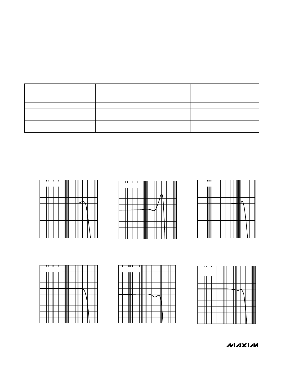
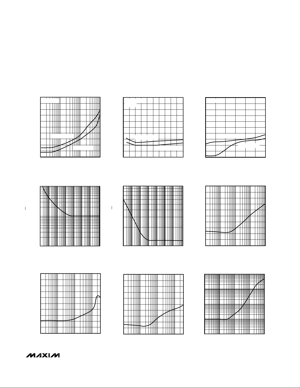
__________________________________________Typical Operating Characteristics
(VCC= 5V, VEE= 0, A
VCL
= 2V/V, RL= 100Ω to VCC/2, TA= +25°C, unless otherwise noted.)
10
0
100k 1M 10M 100M 1G
MAX4214/MAX4215/MAX4217
SMALL-SIGNAL GAIN vs. FREQUENCY
2
MAX4214 toc01
FREQUENCY (Hz)
GAIN (dB)
4
6
8
9
1
3
5
7
V
OUT
= 100mV
P-P
5.5
100k 1M 10M 100M 1G
MAX4214/MAX4215/MAX4217
GAIN FLATNESS vs. FREQUENCY
FREQUENCY (Hz)
5.6
6.5
5.7
MAX4214 toc02
GAIN (dB)
5.9
6.1
6.3
6.4
5.8
6.0
6.2
V
OUT
= 100mV
P-P
10
0
100k 1M 10M 100M 1G
MAX4214/MAX4215/MAX4217
LARGE-SIGNAL GAIN vs. FREQUENCY
2
MAX4214 toc03
FREQUENCY (Hz)
GAIN (dB)
4
6
8
9
1
3
5
7
V
OUT
= 2V
P-P
10
0
100k 1M 10M 100M 1G
MAX4219/MAX4222
SMALL-SIGNAL GAIN vs. FREQUENCY
2
MAX4214 toc04
FREQUENCY (Hz)
GAIN (dB)
4
6
8
9
1
3
5
7
V
OUT
= 100mV
P-P
5.5
100k 1M 10M 100M 1G
MAX4219/MAX4222
GAIN FLATNESS vs. FREQUENCY
FREQUENCY (Hz)
5.6
6.5
5.7
MAX4214 toc05
GAIN (dB)
5.9
6.1
6.3
6.4
5.8
6.0
6.2
V
OUT
= 100mV
P-P
10
0
100k 1M 10M 100M 1G
MAX4219/MAX4222
LARGE-SIGNAL GAIN vs. FREQUENCY
2
MAX4214 toc06
FREQUENCY (Hz)
GAIN (dB)
4
6
8
9
1
3
5
7
V
OUT
= 2V
P-P
RL = 100Ω
AC ELECTRICAL CHARACTERISTICS (continued)
(VCC= 5V, VEE= 0, IN_- = 0, EN_ = 5V, RL= 100Ω to VCC/2, noninverting configuration, TA= T
MIN
to T
MAX
, unless otherwise noted.
Typical values are at T
A
= +25°C.)
All-Hostile Crosstalk X
TALK
MAX4217/MAX4219/MAX4222, f = 10MHz,
V
OUT
= 2V
P-P
dB
PARAMETER SYMBOL MIN TYP MAX UNITS
Buffer Enable Time t
ON
100 ns
-95
Buffer Gain Matching dB
MAX4217/MAX4219/MAX4222, f = 10MHz,
V
OUT
= 100mV
P-P
MAX4215/MAX4219
0.1
Buffer Disable Time t
OFF
1 µsMAX4215/MAX4219
Output Impedance Z
OUT
200 mΩf = 10MHz
CONDITIONS
0
-100
100k 1M 10M 100M
HARMONIC DISTORTION
vs. FREQUENCY
-80
MAX4214 toc07
FREQUENCY (Hz)
HARMONIC DISTORTION (dBc)
-60
-40
-20
-10
-90
-70
-50
-30
V
OUT
= 2V
P-P
2ND HARMONIC
3RD HARMONIC
0
-100
0 100 200 300 400 500 600 700 800 900 1k
HARMONIC DISTORTION
vs. RESISTIVE LOAD
-80
MAX4214 toc08
RESISTIVE LOAD (Ω)
HARMONIC DISTORTION (dBc)
-60
-40
-20
-10
-90
-70
-50
-30
V
OUT
= 2V
P-P
f = 5MHz
2ND HARMONIC
3RD HARMONIC
0
-100
0.5 1.0 1.5 2.0 2.5 3.0 3.5
HARMONIC DISTORTION
vs. VOLTAGE SWING
-80
MAX4214 toc09
VOLTAGE SWING (Vp-p)
HARMONIC DISTORTION (dBc)
-60
-40
-20
-10
-90
-70
-50
-30
f = 5MHz
2ND HARMONIC
3RD HARMONIC
MAX4214/MAX4215/MAX4217/MAX4219/MAX4222
High-Speed, Single-Supply, Gain of 2,
Closed-Loop, Rail-to-Rail Buffers with Enable
_______________________________________________________________________________________ 5
100
10
1
1 10 1k 10M1M
VOLTAGE-NOISE DENSITY
vs. FREQUENCY
MAX4214 toc10
FREQUENCY (Hz)
NOISE (nV/√Hz)
100 10k 100k
10
1
1 10 1k 10M1M
CURRENT-NOISE DENSITY
vs. FREQUENCY
FREQUENCY (Hz)
NOISE (pA/ √Hz)
100 10k 100k
MAX4214 toc11
50
-150
100k 1M 10M 100M 1G
MAX4217/MAX4219/MAX4222
CROSSTALK vs. FREQUENCY
-110
MAX4214 toc12
FREQUENCY (Hz)
CROSSTALK (dB)
-70
-30
10
30
-130
-90
-50
-10
_____________________________Typical Operating Characteristics (continued)
(VCC= 5V, VEE= 0, A
VCL
= 2V/V, RL= 100Ω to VCC/2, TA= +25°C, unless otherwise noted.)
20
-80
100k 1M 10M 100M
POWER-SUPPLY REJECTION
vs. FREQUENCY
-60
MAX4214 toc13
FREQUENCY (Hz)
POWER-SUPPLY REJECTION (dB)
-40
-20
0
10
-70
-50
-30
-10
10
-90
100k 10M 100M1M
MAX4215/MAX4219
OFF-ISOLATION vs. FREQUENCY
-80
MAX4214 toc14
FREQUENCY (Hz)
OFF-ISOLATION (dB)
-70
-60
-50
-40
-30
-20
-10
0
100
0.01
100k 1M 10M 100M 1G
CLOSED-LOOP OUTPUT IMPEDANCE
vs. FREQUENCY
MAX4214 toc15
FREQUENCY (Hz)
IMPEDANCE (Ω)
10
0.1
1
 Loading...