

Page 1
________________General Description
The MAX4200–MAX4205 are ultra-high-speed, openloop buffers featuring high slew rate, high output current, low noise, and excellent capacitive-load-driving
capability. The MAX4200/MAX4201/MAX4202 are single buffers, while the MAX4203/MAX4204/MAX4205 are
dual buffers. The MAX4201/MAX4204 have integrated
50Ω termination resistors, making them ideal for driving 50Ω transmission lines. The MAX4202/MAX4205
include 75Ω back-termination resistors for driving 75Ω transmission lines. The MAX4200/MAX4203
have no internal termination resistors.
The MAX4200–MAX4205 use a proprietary architecture
to achieve up to 780MHz -3dB bandwidth, 280MHz
0.1dB gain flatness, 4200V/µs slew rate, and ±90mA
output current drive capability. They operate from ±5V
supplies and draw only 2.2mA of quiescent current.
These features, along with low-noise performance, make
these buffers suitable for driving high-speed analog-todigital converter (ADC) inputs or for data-communications applications.
________________________Applications
High-Speed DAC Buffers
Wireless LANs
Digital-Transmission Line Drivers
High-Speed ADC Input Buffers
IF/Communications Systems
____________________________Features
♦ 2.2mA Supply Current
♦ High Speed
780MHz -3dB Bandwidth (MAX4201/MAX4202)
280MHz 0.1dB Gain Flatness (MAX4201/MAX4202)
4200V/µs Slew Rate
♦ Low 2.1nV/√Hz Voltage-Noise Density
♦ Low 0.8pA/√Hz Current-Noise Density
♦ High ±90mA Output Drive (MAX4200/MAX4203)
♦ Excellent Capacitive-Load-Driving Capability
♦ Available in Space-Saving SOT23 or µMAX
®
Packages
MAX4200–MAX4205
Ultra-High-Speed, Low-Noise, Low-Power,
SOT23 Open-Loop Buffers
________________________________________________________________ Maxim Integrated Products 1
19-1338; Rev 3; 3/07
_______________Ordering Information
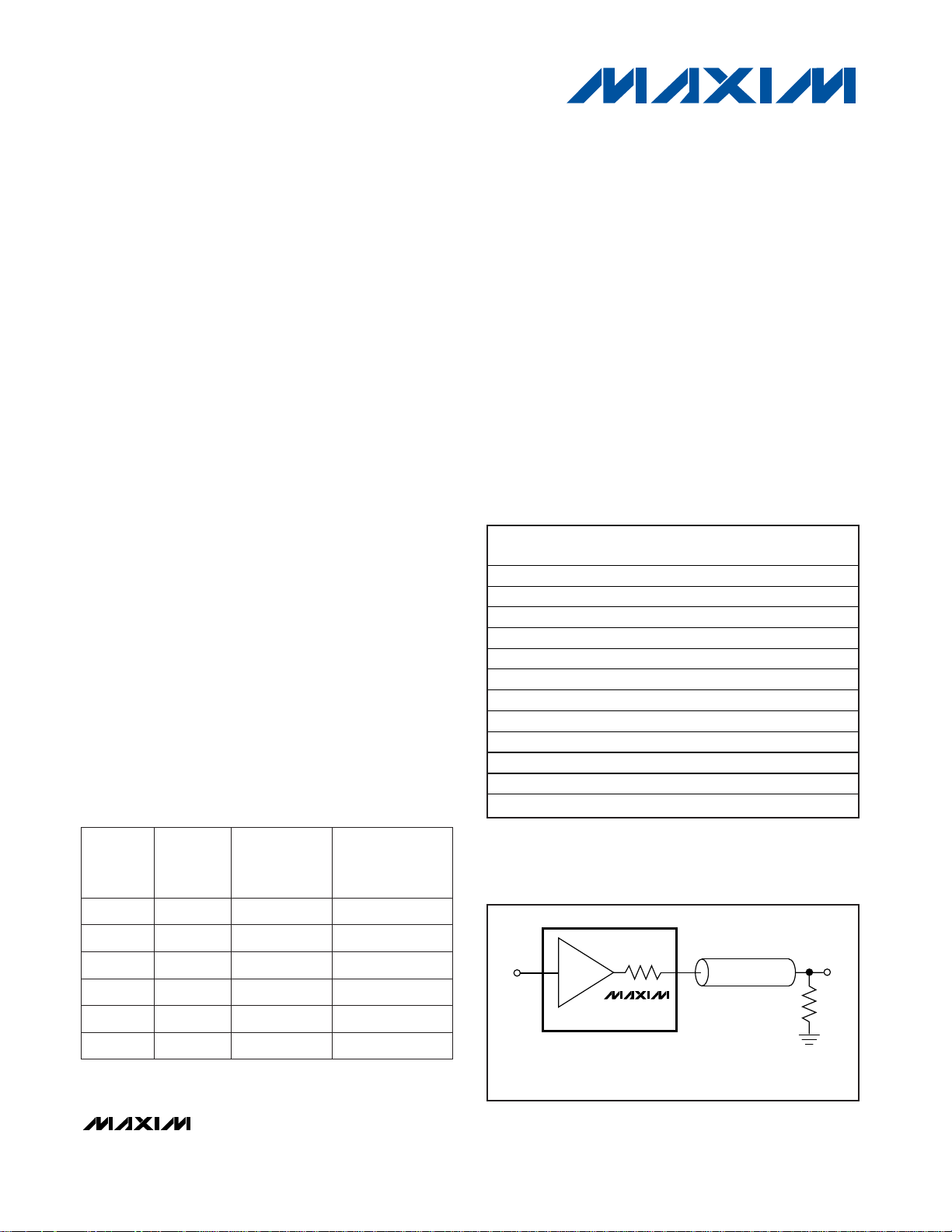
___________Typical Application Circuit
MAX4201
R
EXT
*
50Ω
*R
L
= RT + R
EXT
R
T
*
50Ω
50Ω CABLE
OUTIN
COAXIAL CABLE DRIVER
PART
NO. OF
BUFFERS
INTERNAL
OUTPUT
TERMINATION
(Ω)
PIN-PACKAGE
MAX4204 2 50 8 SO/µMAX
MAX4200 1 — 8 SO, 5 SOT23
MAX4201 1 50 8 SO, 5 SOT23
MAX4205 2 75 8 SO/µMAX
MAX4202 1 75 8 SO, 5 SOT23
MAX4203 2 — 8 SO/µMAX
___________________________Selector Guide
Pin Configurations appear at end of data sheet.
For pricing, delivery, and ordering information, please contact Maxim/Dallas Direct! at
1-888-629-4642, or visit Maxim’s website at www.maxim-ic.com.
µMAX is a registered trademark of Maxim Integrated Products, Inc.
Note: All devices are specified over the -40°C to +85°C operating
temperature range.
PART PIN-PACKAGE
MAX4200ESA 8 SO — S8-2
MAX4200EUK-T 5 SOT23-5 AABZ U5-1
MAX4201ESA 8 SO — S8-2
MAX4201EUK-T 5 SOT23-5 ABAA U5-1
MAX4202ESA 8 SO — S8-2
MAX4202EUK-T 5 SOT23-5 ABAB U5-1
MAX4203ESA 8 SO — S8-2
MAX4203EUA-T 8 µMAX-8 — U8-1
MAX4204ESA 8 SO — S8-2
MAX4204EUA-T 8 µMAX-8 — U8-1
MAX4205ESA 8 SO — S8-2
MAX4205EUA-T 8 µMAX-8 — U8-1
TOP
MARK
PKG
CODE
Page 2
MAX4200–MAX4205
Ultra-High-Speed, Low-Noise, Low-Power,
SOT23 Open-Loop Buffers
2 _______________________________________________________________________________________
ABSOLUTE MAXIMUM RATINGS
DC ELECTRICAL CHARACTERISTICS
(VCC= +5V, VEE= -5V, RL= ∞, TA= T
MIN
to T
MAX
, unless otherwise noted. Typical values are at TA= +25°C.)
Stresses beyond those listed under “Absolute Maximum Ratings” may cause permanent damage to the device. These are stress ratings only, and functional
operation of the device at these or any other conditions beyond those indicated in the operational sections of the specifications is not implied. Exposure to
absolute maximum rating conditions for extended periods may affect device reliability.
Supply Voltage (VCCto VEE)................................................+12V
Voltage on Any Pin to GND..............(V
EE
- 0.3V) to (VCC+ 0.3V)
Output Short-Circuit Duration to GND........................Continuous
Continuous Power Dissipation (T
A
= +70°C)
5-Pin SOT23 (derate 7.1mW/°C above +70°C).............571mW
8-Pin µMAX (derate 4.1mW/°C above +70°C) ..............330mW
8-Pin SO (derate 5.9mW/°C above +70°C)...................471mW
Operating Temperature Range ...........................-40°C to +85°C
Storage Temperature Range .............................-65°C to +150°C
Lead Temperature (soldering, 10s) .................................+300°C
V
IN
= 0V
Sinking or sourcing
Per buffer, VIN= 0V
Guaranteed by PSR test
RL= 30Ω
VS= ±4V to ±5.5V
-3.0V ≤
V
OUT
≤
3.0V
f = DC
VIN= 0V
MAX4203/MAX4204/MAX4205
(Note 1)
CONDITIONS
mA
75
I
SC
Short-Circuit Output
Current
90
150
mA
±44
I
OUT
Output Current ±52
±90
Ω
75
R
OUT
Output Resistance 50
8
mV115V
OS
Input Offset Voltage
mA2.2 4I
S
V±4 ±5.5V
S
Operating Supply Voltage
Quiescent Supply Current
dB55 72PSRPower-Supply Rejection
V/V
0.41 0.50 0.59
A
V
Voltage Gain
0.42 0.50 0.58
0.9 0.96 1.1
µV/°C20TCV
OS
Input Offset Voltage Drift
mV0.4
Input Offset Voltage
Matching
µA0.8 10I
B
Input Bias Current
kΩ500R
IN
Input Resistance
UNITSMIN TYP MAXSYMBOLPARAMETER
MAX4200/MAX4203, R
EXT
= 150Ω
MAX4201/MAX4204, R
EXT
= 50Ω
MAX4202/MAX4205, R
EXT
= 75Ω
MAX4200/MAX4203
MAX4201/MAX4204
MAX4202/MAX4205
MAX4200/MAX4203
MAX4201/MAX4204
MAX4202/MAX4205
MAX4200/MAX4203
MAX4201/MAX4204
MAX4202/MAX4205
MAX4200/MAX4203
RL= 150Ω
VV
OUT
Output-Voltage Swing
±3.3 ±3.8
RL= 100Ω ±3.2 ±3.7
RL= 37.5Ω ±3.3
MAX4201/MAX4204 RL= 50Ω ±1.9 ±2.1
MAX4202/MAX4205 RL= 75Ω ±2.0 ±2.3
Page 3
V
OUT
= 2Vp-p
MAX4200–MAX4205
Ultra-High-Speed, Low-Noise, Low-Power,
SOT23 Open-Loop Buffers
_______________________________________________________________________________________ 3
V
OUT
=
2V
P-P
V
OUT
≤ 100mV
RMS
V
OUT
≤ 100mV
RMS
V
OUT
= 2V step
CONDITIONS
dBc
-32
SFDR
Spurious-Free Dynamic
Range
-44
-47
-34
-45
-48
ns12t
S
Settling Time to 0.1%
ps405Group Delay Time
530
780
660
MHz
310
FPBWFull-Power Bandwidth
490
MHz
230
BW
(0.1dB)
0.1dB Bandwidth
MHz
720
BW
(-3dB)
-3dB Bandwidth
220
280
130
UNITSMIN TYP MAXSYMBOLPARAMETER
AC ELECTRICAL CHARACTERISTICS
(VCC= +5V, VEE= -5V, RL= 100Ω for MAX4200/MAX4201/MAX4203/MAX4204, RL= 150Ω for MAX4202/MAX4205, TA= T
MIN
to
T
MAX
, unless otherwise noted. Typical values are at TA= +25°C.)
f = 1MHz
MAX4200/MAX4201/
MAX4202, f = 500kHz,
V
OUT
= 2V
P-P
pA/√Hz
0.8i
n
Input Current-Noise Density
-48
-48
-72
pF2C
IN
Input Capacitance
V
OUT
= 2V
P-P
f = 10MHz
-65
X
TALK
Amplifier Crosstalk dB
-87
Ω6Z
OUT
Output Impedance
MAX4200
MAX4201/MAX4202
MAX4203
MAX4204/MAX4205
MAX4200
MAX4201/MAX4202
MAX4203
MAX4204/MAX4205
MAX4200/MAX4201/MAX4202
MAX4200/MAX4201/
MAX4202
f = 5MHz
f = 20MHz
f = 100MHz
f = 5MHz
f = 20MHz
f = 100MHz
MAX4203/MAX4204/
MAX4205
V
OUT
≤ 2V
P-P
V
OUT
= 2V step V/µs4200SRSlew Rate
MAX4203/MAX4204/MAX4205
f = 1MHz
NTSC, RL= 150Ω
NTSC, RL= 150Ω
nV/√Hz
2.1e
n
Input Voltage-Noise Density
degrees0.15DPDifferential Phase Error
%1.3DGDifferential Gain Error
Second harmonic
Third harmonic
Total harmonic
Second harmonic
Third harmonic
Total harmonic
MAX4203/MAX4204/|
MAX4205, f = 500kHz,
V
OUT
= 2V
P-P
dBc
-47
HDHarmonic Distortion
-47
-83
f = 10MHz
f = 100MHz
Note 1: Tested with no load; increasing load will decrease input impedance.
Page 4
MAX4200–MAX4205
Ultra-High-Speed, Low-Noise, Low-Power,
SOT23 Open-Loop Buffers
4 _______________________________________________________________________________________
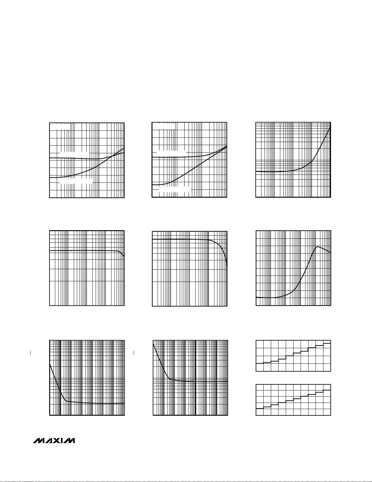
__________________________________________Typical Operating Characteristics
(VCC= +5V, VEE= -5V, RL= 100Ω for MAX4200/MAX4201/MAX4203/MAX4204, RL= 150Ω for MAX4202/MAX4205, unless
otherwise noted.)
4
-6
100k 1M 10M 100M 1G
MAX4200
SMALL-SIGNAL GAIN vs. FREQUENCY
-4
-5
-3
MAX4200/25-01
FREQUENCY (Hz)
NORMALIZED GAIN (dB)
-2
-1
0
2
1
3
V
OUT
= 100mV
P-P
4
-6
100k
1M
10M 100M 1G
MAX4201/MAX4202
SMALL-SIGNAL GAIN vs. FREQUENCY
-4
-5
-3
MAX4200/25-02
FREQUENCY (Hz)
NORMALIZED GAIN (dB)
-2
-1
0
2
1
3
V
OUT
= 100mV
P-P
4
-6
100k
1M
10M 100M 1G
MAX4200/MAX4201/MAX4202
LARGE-SIGNAL GAIN vs. FREQUENCY
-4
-5
-3
MAX4200/25-03
FREQUENCY (Hz)
NORMALIZED GAIN (dB)
-2
-1
0
2
1
3
V
OUT
= 2V
P-P
4
-6
100k 1M 10M
100M
1G
MAX4203
SMALL-SIGNAL GAIN vs. FREQUENCY
-4
-5
-3
MAX4200/25-04
FREQUENCY (Hz)
NORMALIZED GAIN (dB)
-2
-1
0
2
1
3
V
OUT
= 100mV
P-P
5
-5
100k 1M 10M 100M 1G 10G
GROUP DELAY vs. FREQUENCY
-3
-4
-2
MAX4200/25-07
FREQUENCY (Hz)
GROUP DELAY (ns)
-1
0
1
3
2
4
4
-6
100k 1M 10M 100M 1G 10G
MAX4204/MAX4205
SMALL-SIGNAL GAIN vs. FREQUENCY
-4
-5
-3
MAX4200/25-05
FREQUENCY (Hz)
NORMALIZED GAIN (dB)
-2
-1
0
2
1
3
V
OUT
= 100mV
P-P
4
-6
100k 1M 10M 100M 1G
MAX4203/MAX4204/MAX4205
LARGE-SIGNAL GAIN vs. FREQUENCY
-4
-5
-3
MAX4200/25-06
FREQUENCY (Hz)
NORMALIZED GAIN (dB)
-2
-1
0
2
1
3
V
OUT
= 2V
P-P
0
-100
100k 1M 10M 100M 1G 10G
POWER-SUPPLY REJECTION
vs. FREQUENCY
-80
-90
-70
MAX4200/25-08
FREQUENCY (Hz)
PSR (dB)
-60
-50
-40
-20
-30
-10
9000
0
0 1.0 3.02.5 5.0
SLEW RATE vs. OUTPUT VOLTAGE
3000
2000
1000
4000
7000
8000
MAX4200/4205-09
OUTPUT VOLTAGE (Vp-p)
SLEW RATE (V/µs)
1.5 2.00.5 3.5
5000
6000
4.0 4.5
Page 5
MAX4200–MAX4205
Ultra-High-Speed, Low-Noise, Low-Power,
SOT23 Open-Loop Buffers
_______________________________________________________________________________________ 5
0
-10
-100
100k 100M10M1M
MAX4200/MAX4201/MAX4202
HARMONIC DISTORTION vs. FREQUENCY
-60
-70
-80
-90
-30
-40
-50
-20
MAX4200/4205-10
FREQUENCY (Hz)
HARMONIC DISTORTION (dBc)
THIRD HARMONIC
SECOND HARMONIC
VIN = 2Vp-p
0
-10
-100
100k 100M10M1M
MAX4203/MAX4204/MAX4205
HARMONIC DISTORTION vs. FREQUENCY
-60
-70
-80
-90
-30
-40
-50
-20
MAX4200/4205-11
FREQUENCY (Hz)
HARMONIC DISTORTION (dBc)
THIRD HARMONIC
SECOND HARMONIC
V
OUT
= 2Vp-p
100
1
100k 10M 100M1M 1G
MAX4200/MAX4203
OUTPUT IMPEDANCE vs. FREQUENCY
MAX4200/4205-12
FREQUENCY (Hz)
OUTPUT IMPEDANCE (Ω)
10
100
10
100k 10M 100M1M 1G
MAX4201/MAX4204
OUTPUT IMPEDANCE vs. FREQUENCY
MAX4200/4205-13
FREQUENCY (Hz)
OUTPUT IMPEDANCE (Ω)
100
1
1 10 100 1k 10k 100k 1M 10M
INPUT VOLTAGE-NOISE DENSITY
vs. FREQUENCY
MAX4200/4205-16
FREQUENCY (Hz)
VOLTAGE NOISE DENSITY (nV/√Hz)
10
100
10
100k 10M 100M1M 1G
MAX4202/MAX4205
OUTPUT IMPEDANCE vs. FREQUENCY
MAX4200/4205-14
FREQUENCY (Hz)
OUTPUT IMPEDANCE (Ω)
0
-100
100k 1M 10M 100M 1G 10G
MAX4203/MAX4204/MAX4205
CROSSTALK vs. FREQUENCY
-80
-90
MAX4200/4205-15
FREQUENCY (Hz)
CROSSTALK (dB)
-60
-70
-40
-50
-20
-30
-10
10
0.1
1 10 100 1k 10k 100k 1M 10M
INPUT CURRENT-NOISE DENSITY
vs. FREQUENCY
MAX4200/4205-17
FREQUENCY (Hz)
CURRENT NOISE DENSITY (pA/√Hz)
1.0
-0.05
0 100
0100
DIFFERENTIAL GAIN AND PHASE
(R
L
= 150Ω)
-0.5
0
0
0.05
0.5
0.10
1.0
0.20
0.15
1.5
IRE
DIFF PHASE (deg)
DIFF GAIN (%)
MAX4200/4205-18
_________________________________Typical Operating Characteristics (continued)
(VCC= +5V, VEE= -5V, RL= 100Ω for MAX4200/MAX4201/MAX4203/MAX4204, RL= 150Ω for MAX4202/MAX4205, unless
otherwise noted.)
Page 6

MAX4200–MAX4205
Ultra-High-Speed, Low-Noise, Low-Power,
SOT23 Open-Loop Buffers
6 _______________________________________________________________________________________
_________________________________Typical Operating Characteristics (continued)
(VCC= +5V, VEE= -5V, RL= 100Ω for MAX4200/MAX4201/MAX4203/MAX4204, RL= 150Ω for MAX4202/MAX4205, unless
otherwise noted.)
0
4
2
8
6
12
10
14
-5 -3 -2-4 -1012345
GAIN ERROR vs. INPUT VOLTAGE
MAX4200-19
INPUT VOLTAGE (V)
GAIN ERROR (%)
RL = 100Ω
RL = 150Ω
1
3
2
6
5
4
9
8
7
10
0 150 20050 100 250 300 350 400
OUTPUT VOLTAGE SWING vs.
EXTERNAL LOAD RESISTANCE
MAX4200-20
EXTERNAL LOAD RESISTANCE (Ω)
OUTPUT VOLTAGE SWING (V
p-p
)
MAX4200/4203
MAX4201/4204
MAX4202/4205
IN
VOLTAGE
50mV/div
OUT
GND
GND
TIME (5ns/div)
SMALL-SIGNAL PULSE RESPONSE
MAX4200-21
IN
VOLTAGE
50mV/div
OUT
GND
GND
TIME (5ns/div)
MAX4200/MAX4203
SMALL-SIGNAL PULSE RESPONSE
MAX4200-22
C
LOAD
= 15pF
IN
VOLTAGE
50mV/div
OUT
GND
GND
TIME (5ns/div)
MAX4201/MAX4202/MAX4204/MAX4205
SMALL-SIGNAL PULSE RESPONSE
MAX4200-23
C
LOAD
= 22pF
IN
VOLTAGE
1V/div
OUT
GND
GND
TIME (5ns/div)
LARGE-SIGNAL PULSE RESPONSE
MAX4200-24
Page 7

MAX4200–MAX4205
Ultra-High-Speed, Low-Noise, Low-Power,
SOT23 Open-Loop Buffers
_______________________________________________________________________________________ 7
-5
-2
-3
-4
-1
0
1
2
3
4
5
-40 10-15 356085
INPUT OFFSET VOLTAGE
vs. TEMPERATURE
MAX4200-28
TEMPERATURE (°C)
INPUT OFFSET VOLTAGE (mV)
-5
-2
-3
-4
-1
0
1
2
3
4
5
-40 10-15 356085
INPUT BIAS CURRENT
vs. TEMPERATURE
MAX4200-29
TEMPERATURE (°C)
INPUT BIAS CURRENT (µA)
3.0
3.2
3.6
3.4
3.8
4.0
-40 10-15 356085
MAX4200/MAX4203
OUTPUT VOLTAGE SWING
vs. TEMPERATURE
MAX4200-30
TEMPERATURE (°C)
VOLTAGE SWING (Vp-p)
RL = 100Ω
RL = 150Ω
_________________________________Typical Operating Characteristics (continued)
(VCC= +5V, VEE= -5V, RL= 100Ω for MAX4200/MAX4201/MAX4203/MAX4204, RL= 150Ω for MAX4202/MAX4205, unless
otherwise noted.)
IN
VOLTAGE
1V/div
OUT
GND
GND
TIME (5ns/div)
MAX4200/MAX4203
LARGE-SIGNAL PULSE RESPONSE
MAX4200-25
C
LOAD
= 15pF
IN
VOLTAGE
1V/div
OUT
GND
GND
TIME (5ns/div)
MAX4201/MAX4202/MAX4204/MAX4205
LARGE-SIGNAL PULSE RESPONSE
MAX4200-26
C
LOAD
= 22pF
1.0
2.0
1.5
3.0
2.5
3.5
4.0
-40 10-15 356085
SUPPLY CURRENT (PER BUFFER)
vs. TEMPERATURE
MAX4200-27
TEMPERATURE (°C)
SUPPLY CURRENT (mA)
Page 8

_______________Detailed Description
The MAX4200–MAX4205 wide-band, open-loop buffers
feature high slew rates, high output current, low
2.1nV√Hz voltage-noise density, and excellent capacitive-load-driving capability. The MAX4200/MAX4203
are single/dual buffers with up to 660MHz bandwidth,
230MHz 0.1dB gain flatness, and a 4200V/µs slew rate.
The MAX4201/MAX4204 single/dual buffers with integrated 50Ω output termination resistors, up to 780MHz
bandwidth, 280MHz gain flatness, and a 4200V/µs slew
rate, are ideally suited for driving high-speed signals
over 50Ω cables. The MAX4202/MAX4205 provide
bandwidths up to 720MHz, 230MHz gain flatness,
4200V/µs slew rate, and integrated 75Ω output termination resistors for driving 75Ω cables.
With an open-loop gain that is slightly less than +1V/V,
these devices do not have to be compensated with the
internal dominant pole (and its associated phase shift)
that is present in voltage-feedback devices. This feature allows the MAX4200–MAX4205 to achieve a nearly
constant group delay time of 405ps over their full frequency range, making them well suited for a variety of
RF and IF signal-processing applications.
These buffers operate with ±5V supplies and consume
only 2.2mA of quiescent supply current per buffer while
providing up to ±90mA of output current drive capability.
__________Applications Information
Power Supplies
The MAX4200–MAX4205 operate with dual supplies
from ±4V to ±5.5V. Both V
CC
and VEEshould be
bypassed to the ground plane with a 0.1µF capacitor
located as close to the device pin as possible.
Layout Techniques
Maxim recommends using microstrip and stripline techniques to obtain full bandwidth. To ensure that the PC
board does not degrade the amplifier’s performance,
design it for a frequency greater than 6GHz. Pay careful attention to inputs and outputs to avoid large parasitic capacitance. Whether or not you use a
constant-impedance board, observe the following
guidelines when designing the board:
• Do not use wire-wrap boards, because they are too
inductive.
• Do not use IC sockets, because they increase para-
sitic capacitance and inductance.
MAX4200–MAX4205
Ultra-High-Speed, Low-Noise, Low-Power,
SOT23 Open-Loop Buffers
8 _______________________________________________________________________________________
______________________________________________________________Pin Description
No Connection. Not Internally ConnectedN.C.1 1, 2, 5, 8 —
Buffer InputIN3 3 —
Buffer 1 InputIN1— — 1
Buffer 1 OutputOUT1— — 2
Negative Power SupplyV
EE
2 4 —
Negative Power Supply for Buffer 1V
EE1
— — 3
Negative Power Supply for Buffer 2V
EE2
— — 4
Buffer 2 InputIN2— — 5
Buffer 2 OutputOUT2— — 6
Buffer OutputOUT5 6 —
Positive Power SupplyV
CC
4 7 —
Positive Power Supply for Buffer 2V
CC2
— — 7
Positive Power Supply for Buffer 1V
CC1
— — 8
NAME FUNCTION
SOT23-5 SO
SO/µMAX
MAX4200/MAX4201/MAX4202
PIN
MAX4203
MAX4204
MAX4205
Page 9

MAX4200–MAX4205
Ultra-High-Speed, Low-Noise, Low-Power,
SOT23 Open-Loop Buffers
_______________________________________________________________________________________ 9
• Use surface-mount instead of through-hole components for better high-frequency performance.
• Use a PC board with at least two layers; it should be
as free from voids as possible.
• Keep signal lines as short and as straight as possible. Do not make 90° turns; round all corners.
Input Impedance
The MAX4200–MAX4205 input impedance looks like a
500kΩ resistor in parallel with a 2pF capacitor. Since
these devices operate without negative feedback, there
is no loop gain to transform the input impedance
upward, as in closed-loop buffers. As a consequence,
the input impedance is directly related to the output
impedance. If the output load impedance decreases,
the input impedance also decreases. Inductive input
sources (such as an unterminated cable) may react
with the input capacitance and produce some peaking
in the buffer’s frequency response. This effect can usually be minimized by using a properly terminated transmission line at the buffer input, as shown in Figure 1.
Output Current and Gain Sensitivity
The absence of negative feedback means that openloop buffers have no loop gain to reduce their effective
output impedance. As a result, open-loop devices usually suffer from decreasing gain as the output current is
decreased. The MAX4200–MAX4205 include local
feedback around the buffer’s class-AB output stage to
ensure low output impedance and reduce gain sensitivity to load variations. This feedback also produces
demand-driven current bias to the output transistors for
±90mA (MAX4200/MAX4203) drive capability that is relatively independent of the output voltage (see Typical
Operating Characteristics).
Output Capacitive Loading and Stability
The MAX4200–MAX4205 provide maximum AC performance with no load capacitance. This is the case when
the load is a properly terminated transmission line.
However, these devices are designed to drive any load
capacitance without oscillating, but with reduced AC performance.
Since the MAX4200–MAX4205 operate in an open-loop
configuration, there is no negative feedback to be
transformed into positive feedback through phase shift
introduced by a capacitive load. Therefore, these
devices will not oscillate with capacitive loading, unlike
similar buffers operating in a closed-loop configuration.
However, a capacitive load reacting with the buffer’s
output impedance can still affect circuit performance. A
capacitive load will form a lowpass filter with the
buffer’s output resistance, thereby limiting system
bandwidth. With higher capacitive loads, bandwidth is
dominated by the RC network formed by RTand CL;
the bandwidth of the buffer itself is much higher. Also
note that the isolation resistor forms a divider that
decreases the voltage delivered to the load.
Another concern when driving capacitive loads results
from the amplifier’s output impedance, which looks
inductive at high frequency. This inductance forms an
L-C resonant circuit with the capacitive load and causes peaking in the buffer’s frequency response.
Figure 2 shows the frequency response of the
MAX4200/MAX4203 under different capacitive loads. To
settle out some of the peaking, the output requires an isolation resistor like the one shown in Figure 3. Figure 4 is a
plot of the MAX4200/MAX4203 frequency response with
capacitive loading and a 10Ω isolation resistor. In many
applications, the output termination resistors included in
the MAX4201/MAX4202/ MAX4204/MAX4205 will serve
this purpose, reducing component count and board
space. Figure 5 shows the MAX4201/MAX4202/
MAX4204/MAX4205 frequency response with capacitive
loads of 47pF, 68pF, and 120pF.
Coaxial Cable Drivers
Coaxial cable and other transmission lines are easily driven when properly terminated at both ends with their
characteristic impedance. Driving back-terminated
transmission lines essentially eliminates the line’s capacitance. The MAX4201/MAX4204, with their integrated 50Ω
output termination resistors, are ideal for driving 50Ω
cables. The MAX4202/MAX4205 include integrated 75Ω
termination resistors for driving 75Ω cables. Note that the
output termination resistor forms a voltage divider with
the load resistance, thereby decreasing the amplitude of
the signal at the receiving end of the cable by one half
(see the Typical Application Circuit).
MAX42_ _
R
L
50Ω
*MAX4201/4202/4204/4205 ONLY
R
T
*
50Ω COAX
SOURCE
Figure 1. Using a Properly Terminated Input Source
Page 10

MAX4200–MAX4205
Ultra-High-Speed, Low-Noise, Low-Power,
SOT23 Open-Loop Buffers
10 ______________________________________________________________________________________
5
-5
100k 1M
10M
100M 1G
-3
-4
-2
MAX4200-FIG02
FREQUENCY (Hz)
GAIN (dB)
-1
0
1
3
2
4
CL = 47pF
V
OUT
= 100mV
P-P
CL = 68pF
CL = 120pF
CL = 220pF
Figure 2. MAX4200/MAX4203 Small-Signal Gain vs.
Frequency with Load Capacitance and No Isolation Resistor
MAX4200
MAX4203
R
ISO
C
L
V
IN
V
OUT
Figure 3. Driving a Capacitive Load Through an Isolation
Resistor
5
-5
100k 1M
10M
100M 1G
-3
-4
-2
MAX4200-FIG04
FREQUENCY (Hz)
GAIN (dB)
-1
0
1
3
2
4
CL = 47pF
CL = 68pF
CL = 120pF
R
ISO
= 10Ω
V
OUT
= 100mV
P-P
Figure 4. MAX4200/MAX4203 Small-Signal Gain vs.
Frequency with Load Capacitance and 10Ω Isolation Resistor
5
-5
100k 1M 10M 100M 1G
-3
-4
-2
MAX4200-FIG05
FREQUENCY (Hz)
GAIN (dB)
-1
0
1
3
2
4
CL = 47pF
CL = 68pF
CL = 120pF
V
OUT
= 100mV
P-P
Figure 5. MAX4201/MAX4202/MAX4204/MAX4205 SmallSignal Gain vs. Frequency with Capacitive Load and No
External Isolation Resistor
Page 11

MAX4200–MAX4205
Ultra-High-Speed, Low-Noise, Low-Power,
SOT23 Open-Loop Buffers
______________________________________________________________________________________ 11
__________________________________________________________Pin Configurations
TOP VIEW
N.C. = NOT INTERNALLY CONNECTED
* R
T
= 0Ω (MAX4200/MAX4203)
R
T
= 50Ω (MAX4201/MAX4204)
R
T
= 75Ω (MAX4202/MAX4205)
OUT2
V
EE1
IN2V
EE2
1
2
V
CC1
V
CC2
OUT1
IN1
MAX4203
MAX4204
MAX4205
MAX4200
MAX4201
MAX4202
MAX4200
MAX4201
MAX4202
SO/µMAX
3
4
OUT
IN
N.C.
V
EE
1
2
8
7
N.C.
V
CC
N.C.
N.C.
SO
3
4
6
5
V
EE
V
CC
IN
1
5
OUT
N.C.
SOT23-5
2
3
4
*R
T
*R
T
*R
T
*R
T
8
7
6
5
___________________Chip Information
TRANSISTOR COUNTS:
MAX4200/MAX4201/MAX4202: 33
MAX4203/MAX4204/MAX4205: 67
SUBSTRATE CONNECTED TO V
EE
Page 12

MAX4200–MAX4205
Ultra-High-Speed, Low-Noise, Low-Power,
SOT23 Open-Loop Buffers
12 ______________________________________________________________________________________
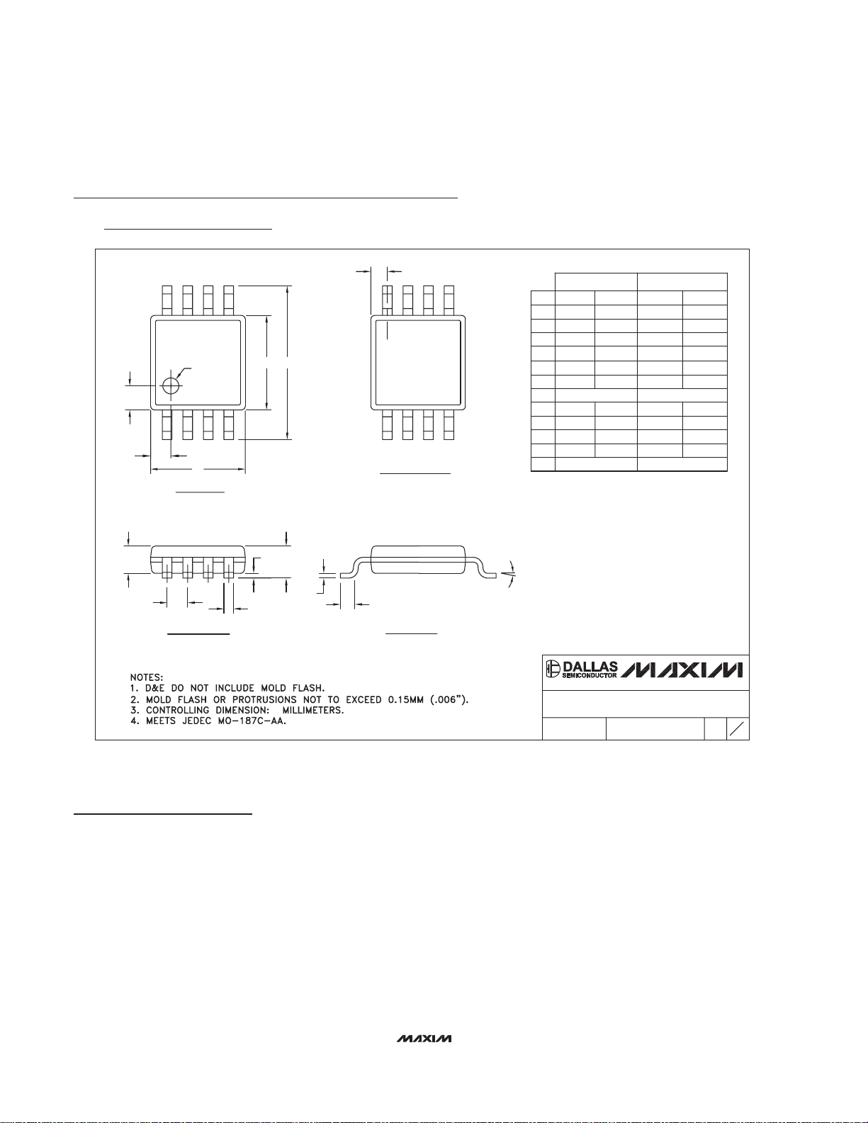
Package Information
(The package drawing(s) in this data sheet may not reflect the most current specifications. For the latest package outline information
go to www.maxim-ic.com/packages
.)
SOICN .EPS
PACKAGE OUTLINE, .150" SOIC
1
1
21-0041
B
REV.DOCUMENT CONTROL NO.APPROVAL
PROPRIETARY INFORMATION
TITLE:
TOP VIEW
FRONT VIEW
MAX
0.010
0.069
0.019
0.157
0.010
INCHES
0.150
0.007
E
C
DIM
0.014
0.004
B
A1
MIN
0.053A
0.19
3.80 4.00
0.25
MILLIMETERS
0.10
0.35
1.35
MIN
0.49
0.25
MAX
1.75
0.050
0.016L
0.40 1.27
0.3940.386D
D
MINDIM
D
INCHES
MAX
9.80 10.00
MILLIMETERS
MIN
MAX
16
AC
0.337 0.344 AB8.758.55 14
0.189 0.197 AA5.004.80 8
N MS012
N
SIDE VIEW
H 0.2440.228 5.80 6.20
e 0.050 BSC 1.27 BSC
C
HE
e
B
A1
A
D
0∞-8∞
L
1
VARIATIONS:
Page 13

MAX4200–MAX4205
Ultra-High-Speed, Low-Noise, Low-Power,
SOT23 Open-Loop Buffers
______________________________________________________________________________________ 13
Package Information (continued)
(The package drawing(s) in this data sheet may not reflect the most current specifications. For the latest package outline information
go to www.maxim-ic.com/packages
.)
SOT-23 5L .EPS
Page 14
MAX4200–MAX4205
Ultra-High-Speed, Low-Noise, Low-Power,
SOT23 Open-Loop Buffers
Maxim cannot assume responsibility for use of any circuitry other than circuitry entirely embodied in a Maxim product. No circuit patent licenses are
implied. Maxim reserves the right to change the circuitry and specifications without notice at any time.
14 ____________________Maxim Integrated Products, 120 San Gabriel Drive, Sunnyvale, CA 94086 408-737-7600
© 2007 Maxim Integrated Products is a registered trademark of Maxim Integrated Products, Inc.
8LUMAXD.EPS
PACKAGE OUTLINE, 8L uMAX/uSOP
1
1
21-0036
J
REV.DOCUMENT CONTROL NO.APPROVAL
PROPRIETARY INFORMATION
TITLE:
MAX
0.043
0.006
0.014
0.120
0.120
0.198
0.026
0.007
0.037
0.0207 BSC
0.0256 BSC
A2
A1
c
e
b
A
L
FRONT VIEW
SIDE VIEW
E H
0.6±0.1
0.6±0.1
Ø0.50±0.1
1
TOP VIEW
D
8
A2
0.030
BOTTOM VIEW
1
6°
S
b
L
H
E
D
e
c
0°
0.010
0.116
0.116
0.188
0.016
0.005
8
4X S
INCHES
-
A1
A
MIN
0.002
0.950.75
0.5250 BSC
0.25 0.36
2.95 3.05
2.95 3.05
4.78
0.41
0.65 BSC
5.03
0.66
6°0°
0.13 0.18
MAX
MIN
MILLIMETERS
- 1.10
0.05 0.15
α
α
DIM
Package Information (continued)
(The package drawing(s) in this data sheet may not reflect the most current specifications. For the latest package outline information
go to www.maxim-ic.com/packages
.)
Revision History
Pages changed at Rev 3: 1–5, 8, 10–14
 Loading...