For free samples & the latest literature: http://www.maxim-ic.com, or phone 1-800-998-8800.
For small orders, phone 1-800-835-8769.
________________General Description
The MAX4200–MAX4205 are ultra-high-speed, openloop buffers featuring high slew rate, high output current, low noise, and excellent capacitive-load-driving
capability. The MAX4200/MAX4201/MAX4202 are single buffers, while the MAX4203/MAX4204/MAX4205 are
dual buffers. The MAX4201/MAX4204 have integrated
50Ω termination resistors, making them ideal for driving 50Ω transmission lines. The MAX4202/MAX4205
include 75Ω back-termination resistors for driving 75Ω transmission lines. The MAX4200/MAX4203
have no internal termination resistors.
The MAX4200–MAX4205 use a proprietary architecture
to achieve up to 780MHz -3dB bandwidth, 280MHz
0.1dB gain flatness, 4200V/µs slew rate, and ±90mA
output current drive capability. They operate from ±5V
supplies and draw only 2.2mA of quiescent current.
These features, along with low-noise performance, make
these buffers suitable for driving high-speed analog-todigital converter (ADC) inputs or for data-communications applications.
________________________Applications
High-Speed DAC Buffers
Wireless LANs
Digital-Transmission Line Drivers
High-Speed ADC Input Buffers
IF/Communications Systems
____________________________Features
♦ 2.2mA Supply Current
♦ High Speed
780MHz -3dB Bandwidth (MAX4201/MAX4202)
280MHz 0.1dB Gain Flatness (MAX4201/MAX4202)
4200V/µs Slew Rate
♦ Low 2.1nV/√Hz Voltage-Noise Density
♦ Low 0.8pA/√Hz Current-Noise Density
♦ High ±90mA Output Drive (MAX4200/MAX4203)
♦ Excellent Capacitive-Load-Driving Capability
♦ Available in Space-Saving SOT23 or µMAX
Packages
MAX4200–MAX4205
Ultra-High-Speed, Low-Noise, Low-Power,
SOT23 Open-Loop Buffers
________________________________________________________________
Maxim Integrated Products
1
19-1338; Rev 2; 4/99
_______________Ordering Information
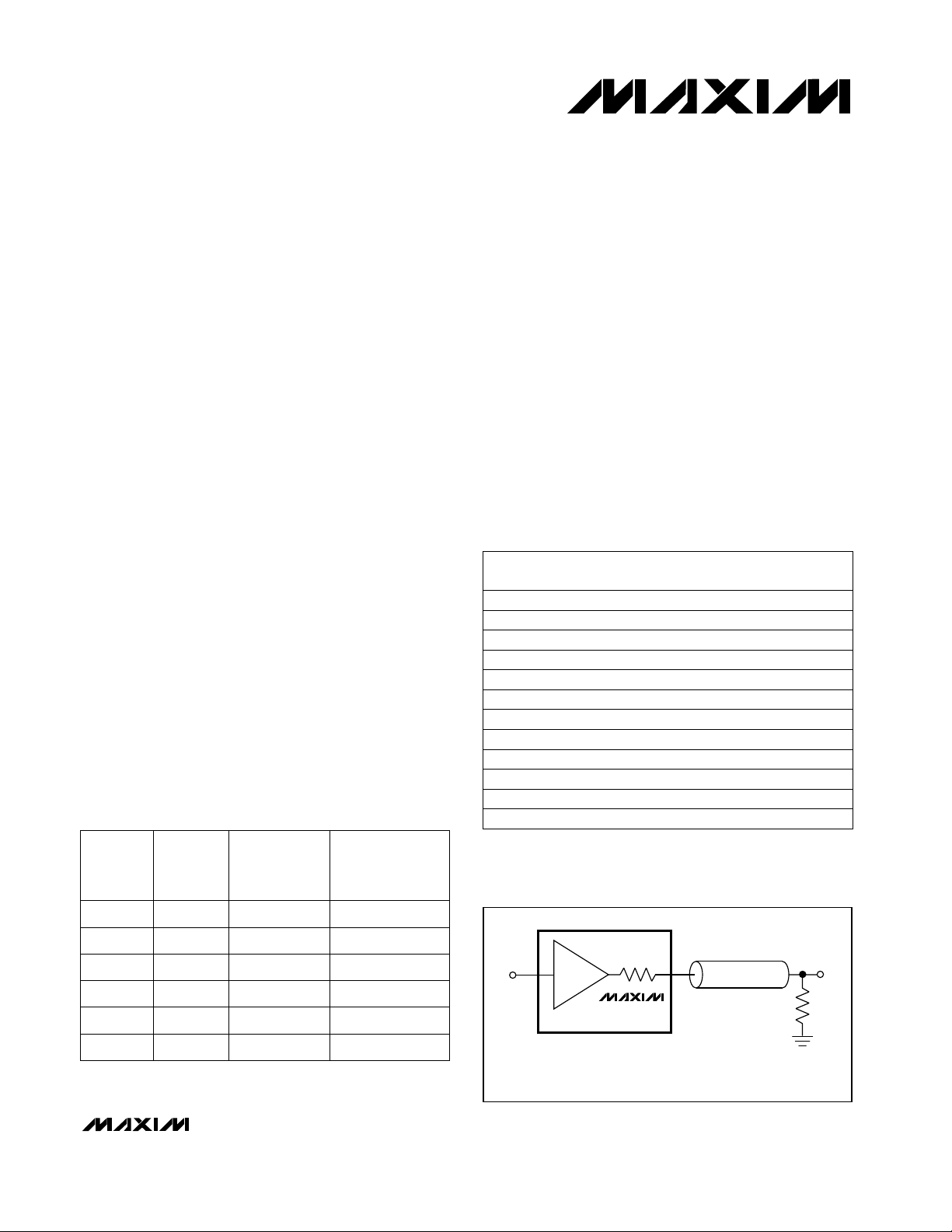
___________Typical Application Circuit
PART
NO. OF
BUFFERS
INTERNAL
OUTPUT
TERMINATION
(Ω)
PIN-PACKAGE
MAX4204 2 50 8 SO/µMAX
MAX4200 1 — 8 SO, 5 SOT23
MAX4201 1 50 8 SO, 5 SOT23
MAX4205 2 75 8 SO/µMAX
MAX4202 1 75 8 SO, 5 SOT23
MAX4203 2 — 8 SO/µMAX
PART
TOP
MARK
MAX4200ESA
—
TEMP. RANGE
PIN-
PACKAGE
-40°C to +85°C 8 SO
MAX4200EUK-T AABZ-40°C to +85°C 5 SOT23-5
MAX4201ESA
—
-40°C to +85°C 8 SO
MAX4201EUK-T ABAA-40°C to +85°C 5 SOT23-5
MAX4202ESA
—
-40°C to +85°C 8 SO
MAX4205EUA—-40°C to +85°C 8 µMAX
MAX4202EUK-T ABAB
MAX4203ESA
—
-40°C to +85°C 5 SOT23-5
-40°C to +85°C 8 SO
MAX4203EUA—-40°C to +85°C 8 µMAX
MAX4204ESA
—
-40°C to +85°C 8 SO
MAX4204EUA—-40°C to +85°C 8 µMAX
MAX4205ESA
—
-40°C to +85°C 8 SO
___________________________Selector Guide
Pin Configurations appear at end of data sheet.
R
*
T
50Ω
MAX4201
50Ω CABLE
R
EXT
50Ω
OUTIN
*
*R
= RT + R
L
EXT
COAXIAL CABLE DRIVER

MAX4200–MAX4205
Ultra-High-Speed, Low-Noise, Low-Power,
SOT23 Open-Loop Buffers
2 _______________________________________________________________________________________
ABSOLUTE MAXIMUM RATINGS
DC ELECTRICAL CHARACTERISTICS
(VCC= +5V, VEE= -5V, RL= ∞, TA= T
MIN
to T
MAX
, unless otherwise noted. Typical values are at TA= +25°C.)
Stresses beyond those listed under “Absolute Maximum Ratings” may cause permanent damage to the device. These are stress ratings only, and functional
operation of the device at these or any other conditions beyond those indicated in the operational sections of the specifications is not implied. Exposure to
absolute maximum rating conditions for extended periods may affect device reliability.
Supply Voltage (VCCto VEE)................................................+12V
Voltage on Any Pin to GND..............(V
EE
- 0.3V) to (VCC+ 0.3V)
Output Short-Circuit Duration to GND........................Continuous
Continuous Power Dissipation (T
A
= +70°C)
5-Pin SOT23 (derate 7.1mW/°C above +70°C).............571mW
8-Pin µMAX (derate 4.1mW/°C above +70°C) ..............330mW
8-Pin SO (derate 5.9mW/°C above +70°C)...................471mW
Operating Temperature Range ...........................-40°C to +85°C
Storage Temperature Range .............................-65°C to +150°C
Lead Temperature (soldering, 10sec) .............................+300°C
VIN= 0V
Sinking or sourcing
Per buffer, VIN= 0V
Guaranteed by PSR test
RL= 30Ω
VS= ±4V to ±5.5V
-3.0V ≤
V
OUT
≤
3.0V
f = DC
VIN= 0V
MAX4203/MAX4204/MAX4205
CONDITIONS
mA
75
I
SC
Short-Circuit Output
Current
90
150
mA
±44
I
OUT
Output Current
±52
±90
Ω
75
R
OUT
Output Resistance 50
8
mV115V
OS
Input Offset Voltage
mA2.2 4I
S
V±4 ±5.5V
S
Operating Supply Voltage
Quiescent Supply Current
dB55 72PSRPower-Supply Rejection
V/V
0.41 0.50 0.59
A
V
Voltage Gain
0.42 0.50 0.58
0.9 0.96 1.1
µV/°C20TCV
OS
Input Offset Voltage Drift
mV0.4
Input Offset Voltage
Matching
µA0.8 10I
B
Input Bias Current
kΩ500R
IN
Input Resistance
UNITSMIN TYP MAXSYMBOLPARAMETER
MAX4200/MAX4203, R
EXT
= 150Ω
MAX4201/MAX4204, R
EXT
= 50Ω
MAX4202/MAX4205, R
EXT
= 75Ω
MAX4200/MAX4203
MAX4201/MAX4204
MAX4202/MAX4205
MAX4200/MAX4203
MAX4201/MAX4204
MAX4202/MAX4205
MAX4200/MAX4203
MAX4201/MAX4204
MAX4202/MAX4205
MAX4200/MAX4203
RL= 150Ω
VV
OUT
Output Voltage Swing
±3.3 ±3.8
RL= 100Ω ±3.2 ±3.7
RL= 37.5Ω ±3.3
MAX4201/MAX4204 RL= 50Ω ±1.9 ±2.1
MAX4202/MAX4205 RL= 75Ω ±2.0 ±2.3

V
OUT
= 2Vp-p
MAX4200–MAX4205
Ultra-High-Speed, Low-Noise, Low-Power,
SOT23 Open-Loop Buffers
_______________________________________________________________________________________ 3
V
OUT
=
2Vp-p
V
OUT
≤ 100mV
RMS
V
OUT
≤ 100mV
RMS
V
OUT
= 2V step
CONDITIONS
dBc
-32
SFDR
Spurious-Free Dynamic
Range
-44
-47
-34
-45
-48
ns12t
S
Settling Time to 0.1%
ps405Group Delay Time
530
780
660
MHz
310
FPBWFull-Power Bandwidth
490
MHz
230
BW
(0.1dB)
0.1dB Bandwidth
MHz
720
BW
(-3dB)
-3dB Bandwidth
220
280
130
UNITSMIN TYP MAXSYMBOLPARAMETER
AC ELECTRICAL CHARACTERISTICS
(VCC= +5V, VEE= -5V, RL= 100Ω for MAX4200/MAX4201/MAX4203/MAX4204, RL= 150Ω for MAX4202/MAX4205, TA= T
MIN
to
T
MAX
, unless otherwise noted. Typical values are at TA= +25°C.)
f = 1MHz
MAX4200/MAX4201/
MAX4202, f = 500kHz,
V
OUT
= 2Vp-p
pA/√Hz
0.8i
n
Input Current Noise Density
-48
-48
-72
pF2C
IN
Input Capacitance
V
OUT
= 2Vp-p
f = 10MHz
-65
X
TALK
Amplifier Crosstalk dB
-87
Ω6Z
OUT
Output Impedance
MAX4200
MAX4201/MAX4202
MAX4203
MAX4204/MAX4205
MAX4200
MAX4201/MAX4202
MAX4203
MAX4204/MAX4205
MAX4200/MAX4201/MAX4202
MAX4200/MAX4201/
MAX4202
f = 5MHz
f = 20MHz
f = 100MHz
f = 5MHz
f = 20MHz
f = 100MHz
MAX4203/MAX4204/
MAX4205
V
OUT
≤ 2Vp-p
V
OUT
= 2V step V/µs4200SRSlew Rate
MAX4203/MAX4204/MAX4205
f = 1MHz
NTSC, RL= 150Ω
NTSC, RL= 150Ω
nV/√Hz
2.1e
n
Input Voltage Noise Density
degrees0.15DPDifferential Phase Error
%1.3DGDifferential Gain Error
Second harmonic
Third harmonic
Total harmonic
Second harmonic
Third harmonic
Total harmonic
MAX4203/MAX4204/|
MAX4205, f = 500kHz,
V
OUT
= 2Vp-p
dBc
-47
HDHarmonic Distortion
-47
-83
f = 10MHz
f = 100MHz

MAX4200–MAX4205
Ultra-High-Speed, Low-Noise, Low-Power,
SOT23 Open-Loop Buffers
4 _______________________________________________________________________________________
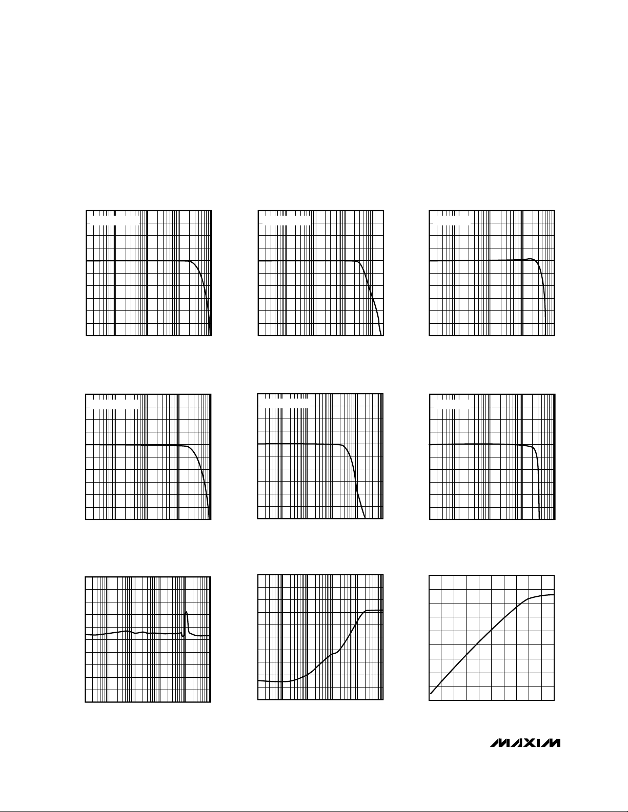
__________________________________________Typical Operating Characteristics
(VCC= +5V, VEE= -5V, RL= 100Ω for MAX4200/MAX4201/MAX4203/MAX4204, RL= 150Ω for MAX4202/MAX4205, unless
otherwise noted.)
4
-6
100k 1M 10M 100M 1G
MAX4200
SMALL-SIGNAL GAIN vs. FREQUENCY
-4
-5
-3
MAX4200/25-01
FREQUENCY (Hz)
NORMALIZED GAIN (dB)
-2
-1
0
2
1
3
V
OUT
= 100mVp-p
4
-6
100k
1M
10M 100M 1G
MAX4201/MAX4202
SMALL-SIGNAL GAIN vs. FREQUENCY
-4
-5
-3
MAX4200/25-02
FREQUENCY (Hz)
NORMALIZED GAIN (dB)
-2
-1
0
2
1
3
V
OUT
= 100mVp-p
4
-6
100k
1M
10M 100M 1G
MAX4200/MAX4201/MAX4202
LARGE-SIGNAL GAIN vs. FREQUENCY
-4
-5
-3
MAX4200/25-03
FREQUENCY (Hz)
NORMALIZED GAIN (dB)
-2
-1
0
2
1
3
V
OUT
= 2Vp-p
4
-6
100k 1M 10M
100M
1G
MAX4203
SMALL-SIGNAL GAIN vs. FREQUENCY
-4
-5
-3
MAX4200/25-04
FREQUENCY (Hz)
NORMALIZED GAIN (dB)
-2
-1
0
2
1
3
V
OUT
= 100mVp-p
5
-5
100k 1M 10M 100M 1G 10G
GROUP DELAY vs. FREQUENCY
-3
-4
-2
MAX4200/25-07
FREQUENCY (Hz)
GROUP DELAY (ns)
-1
0
1
3
2
4
4
-6
100k 1M 10M 100M 1G 10G
MAX4204/MAX4205
SMALL-SIGNAL GAIN vs. FREQUENCY
-4
-5
-3
MAX4200/25-05
FREQUENCY (Hz)
NORMALIZED GAIN (dB)
-2
-1
0
2
1
3
V
OUT
= 100mVp-p
4
-6
100k 1M 10M 100M 1G
MAX4203/MAX4204/MAX4205
LARGE-SIGNAL GAIN vs. FREQUENCY
-4
-5
-3
MAX4200/25-06
FREQUENCY (Hz)
NORMALIZED GAIN (dB)
-2
-1
0
2
1
3
V
OUT
= 2Vp-p
0
-100
100k 1M 10M 100M 1G 10G
POWER-SUPPLY REJECTION
vs. FREQUENCY
-80
-90
-70
MAX4200/25-08
FREQUENCY (Hz)
PSR (dB)
-60
-50
-40
-20
-30
-10
9000
0
0 1.0 3.02.5 5.0
SLEW RATE vs. OUTPUT VOLTAGE
3000
2000
1000
4000
7000
8000
MAX4200/4205-09
OUTPUT VOLTAGE (Vp-p)
SLEW RATE (V/µs)
1.5 2.00.5 3.5
5000
6000
4.0 4.5
 Loading...