Maxim MAX4196ESA, MAX4195ESA, MAX4194ESA, MAX4197ESA Datasheet

For free samples & the latest literature: http://www.maxim-ic.com, or phone 1-800-998-8800.
For small orders, phone 1-800-835-8769.
General Description
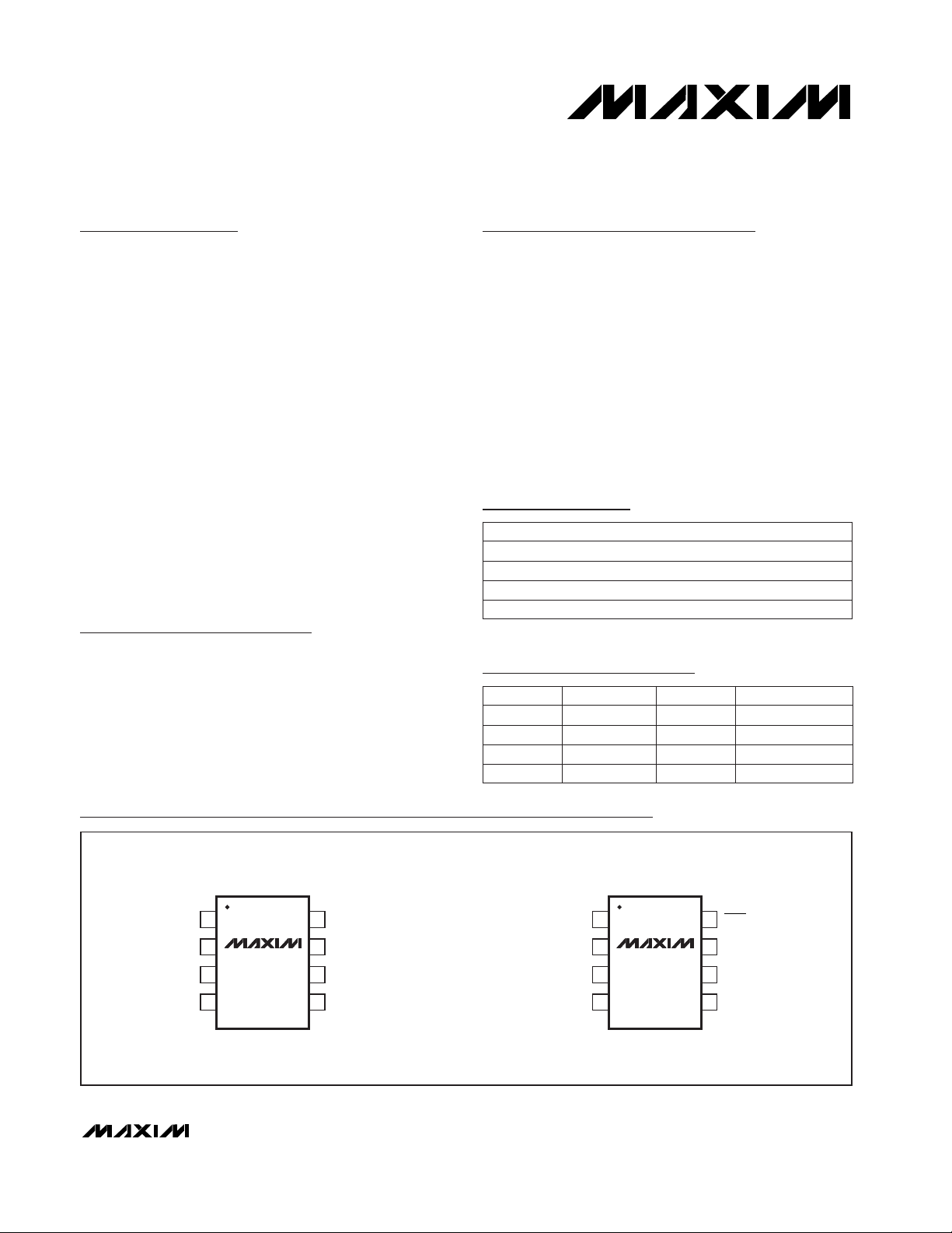
The MAX4194 is a variable-gain precision instrumentation amplifier that combines Rail-to-Rail®single-supply
operation, outstanding precision specifications, and a
high gain bandwidth. This amplifier is also offered in
three fixed-gain versions: the MAX4195 (G = +1V/V),
the MAX4196 (G = +10V/V), and the MAX4197 (G =
+100V/V). The fixed-gain instrumentation amplifiers feature a shutdown function that reduces the quiescent
current to 8µA. A traditional three operational amplifier
configuration is used to achieve maximum DC precision.
The MAX4194–MAX4197 have rail-to-rail outputs and
inputs that can swing to within 200mV of the negative rail
and to within 1.1V of the positive rail. All parts draw only
93µA and operate from a single +2.7V to +7.5V supply
or from dual ±1.35V to ±3.75V supplies. These amplifiers
are offered in 8-pin SO packages and are specified for
the extended temperature range (-40°C to +85°C).
See the MAX4198/MAX4199 data sheet for single-supply, precision differential amplifiers.
Applications
Medical Equipment
Thermocouple Amplifier
4–20mA Loop Transmitters
Data-Acquisition Systems
Battery-Powered/Portable Equipment
Transducer Interface
Bridge Amplifier
Features
♦ +2.7V Single-Supply Operation
♦ Low Power Consumption
93µA Supply Current
8µA Shutdown Current (MAX4195/96/97)
♦ High Common-Mode Rejection: 115dB (G = +10V/V)
♦ Low 50µV Input Offset Voltage (G ≥ +100V/V)
♦ Low ±0.01% Gain Error (G = +1V/V)
♦ 250kHz -3dB Bandwidth (G = +1V/V, MAX4194)
♦ Rail-to-Rail Outputs
MAX4194–MAX4197
Micropower, Single-Supply, Rail-to-Rail,
Precision Instrumentation Amplifiers
________________________________________________________________
Maxim Integrated Products
1
OUT
REFV
EE
1
2
87RG+
V
CC
IN-
IN+
RG-
SO
TOP VIEW
3
4
6
5
MAX4194
OUT
FBV
EE
1
2
87SHDN
V
CC
IN-
IN+
REF
SO
3
4
6
5
MAX4195
MAX4196
MAX4197
19-1468; Rev 0; 4/99
PART
MAX4194ESA
MAX4195ESA
MAX4196ESA
-40°C to +85°C
-40°C to +85°C
-40°C to +85°C
TEMP. RANGE PIN-PACKAGE
8 SO
8 SO
8 SO
Pin Configurations
Ordering Information
MAX4197ESA
-40°C to +85°C 8 SO
PART
MAX4194
MAX4195
MAX4196 Yes
Yes
No
SHUTDOWN GAIN (V/V)
Variable
+1
+10
MAX4197 Yes +100
Selector Guide
Rail-to-Rail is a registered trademark of Nippon Motorola, Ltd.
CMRR (dB)
95 (G = +1V/V)
95
115
115

MAX4194–MAX4197
Micropower, Single-Supply, Rail-to-Rail,
Precision Instrumentation Amplifiers
2 _______________________________________________________________________________________
ABSOLUTE MAXIMUM RATINGS
ELECTRICAL CHARACTERISTICS
(VCC= +5V, VEE= 0, RL= 25kΩ tied to VCC/2, V
REF
= VCC/2, TA= T
MIN
to T
MAX
, unless otherwise noted. Typical values are at
T
A
= +25°C.)
Stresses beyond those listed under “Absolute Maximum Ratings” may cause permanent damage to the device. These are stress ratings only, and functional
operation of the device at these or any other conditions beyond those indicated in the operational sections of the specifications is not implied. Exposure to
absolute maximum rating conditions for extended periods may affect device reliability.
Supply Voltage (VCCto VEE)..................................................+8V
All Other Pins ..................................(VCC+ 0.3V) to (VEE- 0.3V)
Current into Any Pin..........................................................±30mA
Output Short-Circuit Duration (to VCCor VEE)........... Continuous
Continuous Power Dissipation (TA= +70°C)
SO (derate 5.9mW/°C above +70°C)........................... 471mW
Operating Temperature Range ...........................-40°C to +85°C
Junction Temperature......................................................+150°C
Storage Temperature Range.............................-65°C to +150°C
Lead Temperature (soldering, 10sec)............................ +300°C
I
SHDN
= VIL, MAX4195/96/97 only µA
Inferred by PSR
test
VCM= VEE+ 0.2V
to VCC- 1.1V,
f = 120Hz
VCM= VEE+ 0.2V
to VCC- 1.1V,
TA= T
MIN
to T
MAX
,
∆RS= 1kΩ
115
VCM= VCC/2
Differential
90 115
VCM= VEE+ 0.2V
to V
CC
- 1.1V,
T
A
= +25°C,
∆R
S
= 1kΩ
G = +1V/V
Common mode
VIN+ = VIN- = VCC/2, V
DIFF
= 0
G = +1V/V, VCM= VCC/2, TA= +25°C
Inferred from CMR test
VCM= VCC/2
CONDITIONS
106
101
dB
85
CMR
AC
AC Common-Mode Rejection
88 115
115
G = +1V/V
73 95
G = +10V/V
95 115
G = +100V/V
G = +1V/V
G = +10V/V
93 115
G = +100V/V
G = +1000V/V
dB
78 95
CMR
DC
DC Common-Mode Rejection
VVEE+ 0.2 VCC- 1.1V
IN
Input Voltage Range
Differential
1000
Common mode 4
812
I
SHDN
Shutdown Current
V
±1.35 ±3.75
pF
2.7 7.5
V
CC
Supply Voltage Range
1
MΩ
1000
R
IN
Input Resistance
C
IN
Input Capacitance
G = +1V/V
G = +10V/V
µV/°C
±1.0 ±4.0
TC
VOS
Input Offset Voltage Drift
(Note 1)
µA
93 110
I
CC
Quiescent Current
G = +100V/V
±100 ±450
G = +1000V/V
UNITSMIN TYP MAXSYMBOLPARAMETER
Single supply
Dual supplies
G ≥ +10V/V ±0.5 ±2.0
G = +10V/V, VCM= VCC/2, TA= +25°C
±75 ±225
G = +1000V/V, VCM= VCC/2, TA= +25°C
±50
G = +100V/V, VCM= VCC/2, TA= +25°C
±50 ±225
G = +10V/V, VCM= VCC/2, TA= T
MIN
to T
MAX
±75 ±345
G = +1V/V, VCM= VCC/2, TA= T
MIN
to T
MAX
G = +1000V/V, VCM= VCC/2, TA= T
MIN
to
µVV
OS
Input Offset Voltage
±50
G = +100V/V, VCM= VCC/2, TA= T
MIN
to
±50 ±345
±100 ±690

MAX4194–MAX4197
Micropower, Single-Supply, Rail-to-Rail,
Precision Instrumentation Amplifiers
_______________________________________________________________________________________ 3
ELECTRICAL CHARACTERISTICS (continued)
(VCC= +5V, VEE= 0, RL= 25kΩ tied to VCC/2, V
REF
= VCC/2, TA= T
MIN
to T
MAX
, unless otherwise noted. Typical values are at
T
A
= +25°C.)
VCM= VCC/2
VCM= VCC/2
+2.7V ≤ VCC≤ +7.5V; VCM= +1.5V;
V
OUT
= +1.5V; V
REF
= +1.5V; RL= 25kΩ to
+1.5V; G = +1V/V, +10V/V, +100V/V
RL= 25kΩ to VCC/2
MAX4194 only
f = 0.1Hz to 10Hz
f = 10kHz
VCM= VCC/2
f = 10Hz
RL= 5kΩ to VCC/2
f = 100Hz
CONDITIONS
±0.01 ±0.1
1+ (50kΩ/RG)Gain Equation
mA±4.5I
SC
Short-Circuit Current (Note 2)
mV
100 200
VOH, V
OL
Output Voltage Swing
100 200
nA±1.0 ±3.0I
OS
Input Offset Current
pA/°C15TC
IB
dB90 120PSRPower-Supply Rejection
Input Bias Current Drift
30 100
30 100
pA
RMS
16
i
n
Input Noise Current
pA√Hz
0.1
pA/°C15TC
IOS
Input Offset Current Drift
85
2.4
0.76
UNITSMIN TYP MAXSYMBOLPARAMETER
f = 10Hz
75f = 100Hz
nV√Hz
72f = 10KHz
G = +1V/V
µV
RMS
1.4f = 0.1Hz to 10Hz
35f = 10Hz
32f = 100Hz
nV√Hz
31f = 10KHz
G = +10V/V
µV
RMS
0.7f = 0.1Hz to 10Hz
32f = 10Hz
31f = 100Hz
nV√Hz
8.7f = 10KHz
G = +100V/V
µV
RMS
0.6
e
n
Input Noise Voltage
f = 0.1Hz to 10Hz
VCC- V
OH
V
OL
VCC- V
OH
V
OL
G = +1V/V
G = +10V/V ±0.03 ±0.3
TA= +25°C,
VCM= VCC/2,
RL= 25kΩ,
VEE+ 0.1V ≤ V
OUT
≤ VCC- 0.1V
G = +1000V/V, MAX4194 ±0.5
G = +100V/V ±0.05 ±0.5
G = +10V/V ±0.03 ±0.3
TA= +25°C,
VCM= VCC/2,
RL= 5kΩ,
VEE+ 0.2V ≤ V
OUT
≤ VCC- 0.2V
G = +1000V/V, MAX4194
G = +1V/V
%
±0.5
Gain Error
G = +100V/V ±0.05 ±0.5
±0.01 ±0.1
VCM= VCC/2 nA620I
B
Input Bias Current

MAX4194–MAX4197
Micropower, Single-Supply, Rail-to-Rail,
Precision Instrumentation Amplifiers
4 _______________________________________________________________________________________
Note 1: Guaranteed by design.
Note 2: Maximum output current (sinking/sourcing) in which the gain changes by less than 0.1%.
Note 3: This specification represents the typical temperature coefficient of an on-chip thin film resistor. In practice, the temperature
coefficient of the gain for the MAX4194 will be dominated by the temperature coefficient of the external gain-setting resistor.
ELECTRICAL CHARACTERISTICS (continued)
(VCC= +5V, VEE= 0, RL= 25kΩ tied to VCC/2, V
REF
= VCC/2, TA= T
MIN
to T
MAX
, unless otherwise noted. Typical values are at
T
A
= +25°C.)
V
SHDN
= VCC- 2.5V to VCC- 1.5V, G = +100V/V,
0.1%, V
OUT
= +3.5V
G = +1V/V, 0.1%, V
OUT
= +3.5V
MAX4196/MAX4197
G = +1V/V, 0.1%,
V
OUT
= +3.5V
MAX4194/MAX4195, G = +1V/V
G = +1V/V, 0.1%,
V
OUT
= +3V
VEE< V
SHDN
< V
CC
V
OUT
= 2Vp-p, G = +1V/V, f = 1kHz
V
OUT
= 2Vp-p, G = +1V/V
MAX4194
VEE+ 0.1V ≤ V
OUT
≤ VCC- 0.1V, VCM= VCC/2,
G = +1V/V, +10V/V, +100V/V, +1000V/V
0.1%, V
OUT
= 2Vp-p
CONDITIONS
ms0.5t
ON/OFF
On/Off Settling Time
ms1Power-Up Delay
ms0.5t
ENABLE
Enable Time From Shutdown
ms0.5t
SHDN
Time to Shutdown
µA±0.1
SHDN Input Current
VVCC- 2.5V
IL
Input Logic Voltage Low
VVCC- 1.5V
IH
Input Logic Voltage High
%0.001THDTotal Harmonic Distortion
ms
7
t
S
Settling Time
5
ppm/°C±16
ppm/°C
±1 ±15
±1 ±8
Gain Temperature Coefficient
(Note 1)
0.04
0.05
V/µs0.06SRSlew Rate
250
TC
50kΩ
50kΩ Resistance Temperature
Coefficient (Note 3)
%±0.001Nonlinearity
pF300C
L
Capacitive Load Stability
UNITSMIN TYP MAXSYMBOLPARAMETER
MAX4194
G = +1V/V
MAX4195 220
MAX4194
G = +10V/V
MAX4196
17
34
MAX4194 1.5
G = +100V/V
MAX4197
G = +1000V/V
V
OUT
≤ 0.1Vp-p,
VCM= VCC/2
MAX4194
kHz
3.1
0.147
BW-
3dB
-3dB Bandwidth
G = +1V/V
G = +10V/V
G = +100V/V
G = +1000V/V
MAX4195/MAX4196/
MAX4197 only
MAX4195/MAX4196/
MAX4197 only
MAX4195/MAX4196/
MAX4197 only
 Loading...