

Datasheet MAX4275BEESA, MAX4275BDEUA, MAX4275BDESA, MAX4275BCEUA, MAX4275BCESA Datasheet (Maxim)
...
For free samples & the latest literature: http://www.maxim-ic.com, or phone 1-800-998-8800.
For small orders, phone 1-800-835-8769.
General Description
The MAX4174/MAX4175/MAX4274/MAX4275 GainAmp™ family combines a low-cost Rail-to-Rail®op amp
with precision internal gain-setting resistors and VCC/ 2
biasing. Factory-trimmed on-chip resistors decrease
design size, cost, and layout, and provide 0.1% gain
accuracy. Fixed inverting gains from -0.25V/V to
-100V/V or noninverting gains from +1.25V/V to
+101V/V are available. These devices operate from a
single +2.5V to +5.5V supply and consume only 300µA.
GainAmp amplifiers are optimally compensated for
each gain version, achieving exceptional GBW products up to 23MHz (AV= +25V/V to +101V/V). High-voltage fault protection withstands ±17V at either input
without excessive current draw.
Three versions are available in this amplifier family: single/
dual/quad open-loop, unity-gain stable (MAX4281/
MAX4282/MAX4284); single/dual fixed gain (MAX4174/
MAX4274); and single/dual fixed gain plus internal
VCC/ 2 bias at the noninverting input (MAX4175/
MAX4275), which simplifies input biasing in single-supply
designs. The input common-mode voltage range of the
open-loop amplifiers extends from 150mV below the
negative supply to within 1.2V of the positive supply.
The outputs can swing rail-to-rail and drive a 1kΩ load
while maintaining excellent DC accuracy. The amplifier
is stable for capacitive loads up to 470pF.
Applications
Portable Instruments Smart-Card Readers
Instruments, Terminals, Infrared Receivers for
and Bar-Code Readers Remote Controls
Keyless Entry Low-Side Current-Sense
Photodiode Preamps
Amplifiers
Features
♦ GainAmp Family Provides Internal Precision
Gain-Setting Resistors in SOT23 (MAX4174/5)
♦ 0.1% Gain Accuracy (R
F/RG
) (MAX4174/5,
MAX4274/5)
♦ 54 Standard Gains Available (MAX4174/5,
MAX4274/5)
♦ Open-Loop Unity-Gain-Stable Op Amps
(MAX4281/2/4)
♦ Rail-to-Rail Outputs Drive 1kΩ Load
♦ Internal V
CC
/ 2 Biasing (MAX4175/MAX4275)
♦ +2.5V to +5.5V Single Supply
♦ 300µA Supply Current
♦ Up to 23MHz GBW Product
♦ Fault-Protected Inputs Withstand ±17V
♦ Stable with Capacitive Loads Up to 470pF with
No Isolation Resistor
MAX4174/5, MAX4274/5, MAX4281/2/4
†
SOT23, Rail-to-Rail, Fixed-Gain
GainAmps/Open-Loop Op Amps
________________________________________________________________
Maxim Integrated Products
1
19-1407; Rev 3; 8/99
PART*
MAX4174_EUK-T
-40°C to +85°C
TEMP. RANGE
PIN-
PACKAGE
5 SOT23-5
Ordering Information continued at end of data sheet.
*
Insert the desired gain code (from the Gain Selection Guide)
in the blank to complete the part number.
††
Refer to the Gain Selection Guide for a list of preferred gains
and SOT Top Marks.
Ordering Information
GainAmp is a trademark of Maxim Integrated Products. Rail-to-Rail is a registered trademark of Nippon Motorola, Ltd.
†
Patent pending
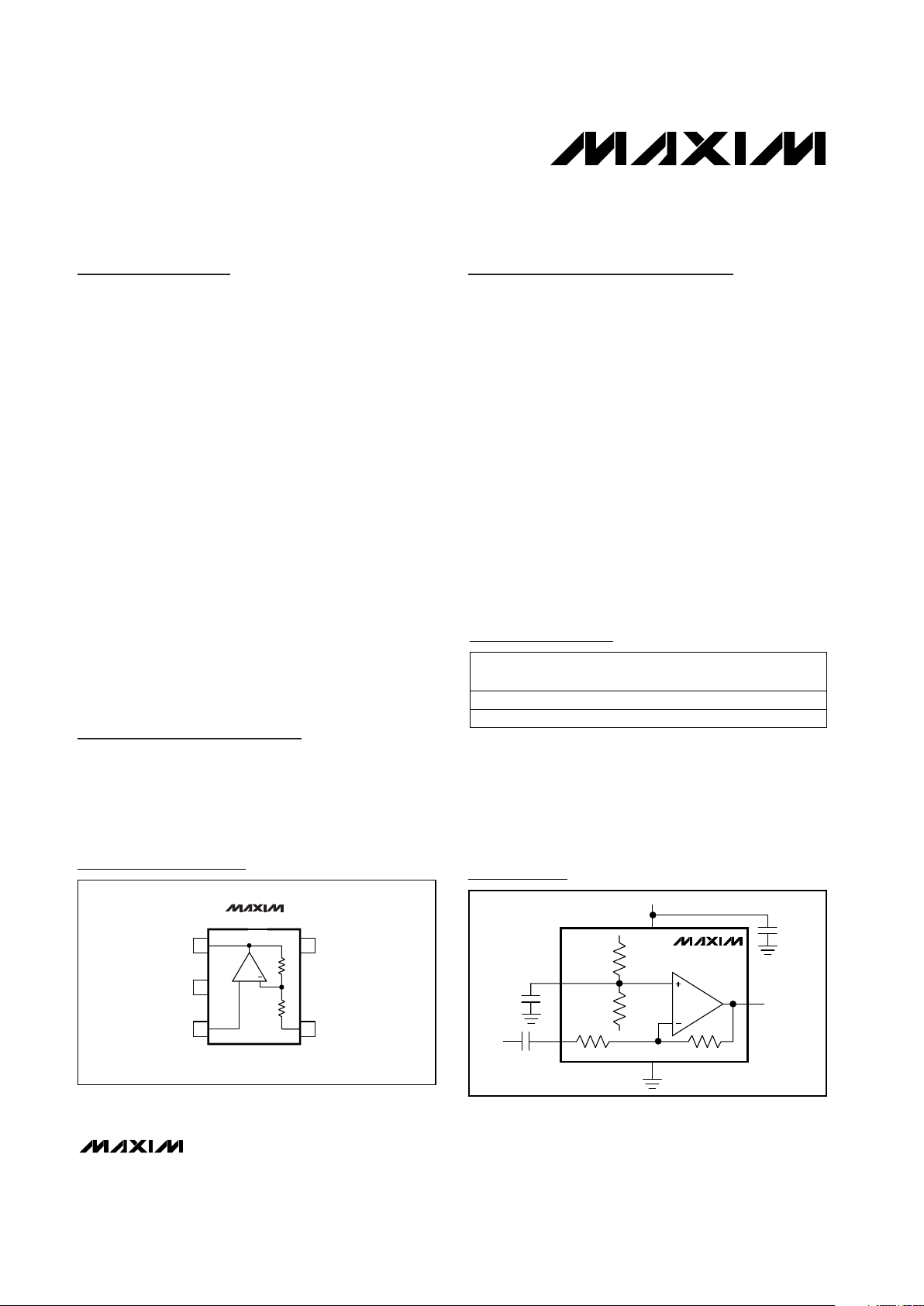
Pin Configurations
Typical Operating Circuit
MAX4175
INPUT
IN-
IN+
+5V
R
B
R
B
OUT
V
CC
V
CC
V
EE
V
EE
R
G
0.1µF
R
F
0.1µF
0.1µF
TOP VIEW
MAX4174
5
4
1
2
3
IN-
OUT
V
CC
V
EE
R
G
R
F
IN+
+
SOT23-5
Selector Guide appears at end of data sheet.
Pin Configurations continued at end of data sheet.
TOP
MARK
††
MAX4175_EUK-T
††
-40°C to +85°C 5 SOT23-5
MAX4174/5, MAX4274/5, MAX4281/2/4
SOT23, Rail-to-Rail, Fixed-Gain
GainAmps/Open-Loop Op Amps
2 _______________________________________________________________________________________
ABSOLUTE MAXIMUM RATINGS
ELECTRICAL CHARACTERISTICS—MAX4174/MAX4175/MAX4274/MAX4275 Fixed-Gain
Amplifiers
(VCC= +2.5V to +5.5V, VEE= 0, V
IN+
= V
IN-
= VCC/ 2, RLto VCC/ 2, RL= open, TA= T
MIN
to T
MAX
, unless otherwise noted. Typical
values are at V
CC
= +5V and TA= +25°C.) (Note 1)
Stresses beyond those listed under “Absolute Maximum Ratings” may cause permanent damage to the device. These are stress ratings only, and functional
operation of the device at these or any other conditions beyond those indicated in the operational sections of the specifications is not implied. Exposure to
absolute maximum rating conditions for extended periods may affect device reliability.
Supply Voltage (VCCto VEE) ....................................-0.3V to +6V
Voltage Inputs (IN_)
MAX4281/4282/4284.....................(V
EE
- 0.3V) to (VCC+ 0.3V)
MAX4174/4175/4274/4275 (with respect to GND) ...........±17V
Output Short-Circuit Duration
(OUT_).....................................Continuous to Either V
EE
or V
CC
Continuous Power Dissipation (TA= +70°C)
5-Pin SOT23 (derate 7.1mW/°C above +70°C).............571mW
8-Pin SO (derate 5.88mW/°C above +70°C).................471mW
8-Pin µMAX (derate 4.1mW/°C above +70°C) ............330mW
14-Pin SO (derate 8.3mW/°C above +70°C)...............667mW
16-Pin QSOP (derate 8.3mW/°C above +70°C)..........667mW
Operating Temperature Range ...........................-40°C to +85°C
Maximum Junction Temperature .....................................+150°C
Storage Temperature Range .............................-65°C to +150°C
Lead Temperature (soldering, 10sec) .............................+300°C
RL= 1kΩ
RL= 100kΩ
MAX4174/MAX4274
Shorted to V
CC
Shorted to V
EE
Guaranteed by PSRR tests
VCC= 2.5V to 5.5V
IN_+, MAX4174/MAX4274 (Note 2)
MAX4175/MAX4275
MAX4175/MAX4275,
includes V
CC
/ 2 bias resistors
MAX4174/MAX4274
RL= 100kΩ
CONDITIONS
mV
60 150
Output Voltage Swing
(Note 4)
150 250
28
28
VOH/V
OL
mA
65
Short-Circuit Current
10
Ω0.02R
OUT
Closed-Loop Output
Impedance
dB70 90PSRR
Power-Supply Rejection
Ratio
kΩ75
Noninverting Input
Resistance
MΩ1000
330 510
300 460
V2.5 5.5V
CC
Supply Voltage Range
150
nA±0.05 ±10I
BIAS
Input Bias Current
µV/°CInput Offset Voltage Drift ±5
320 480
µA
355 530
I
CC
Supply Current
(per Amplifier)
±0.5 ±2.5
UNITSMIN TYP MAXSYMBOLPARAMETER
VCC= 3V
VCC= 5V
VCC= 3V
VCC= 5V
mVV
OS
Input Offset Voltage
AV< 25V/V
kΩ
40
Inverting Input Resistance
AV> 25V/V
VCC- V
OH
VOL- V
EE
VCC- V
OH
VOL- V
EE
MAX4175/MAX4275, VIN+ = VIN- V
V
CC
/ 2 VCC/ 2
- 0.25 + 0.25
IN_+ Bias Voltage
Guaranteed by functional test (Note 3) VV
EE
VCC- 1.2IN_+ Input Voltage Range
Guaranteed by functional test VV
EE
V
CC
IN_- Input Voltage Range
MAX4174/5, MAX4274/5, MAX4281/2/4
SOT23, Rail-to-Rail, Fixed-Gain
GainAmps/Open-Loop Op Amps
_______________________________________________________________________________________ 3
ELECTRICAL CHARACTERISTICS—MAX4174/MAX4175/MAX4274/MAX4275 Fixed-Gain
Amplifiers (continued)
(VCC= +2.5V to +5.5V, VEE= 0, V
IN+
= V
IN-
= VCC/ 2, RLto VCC/ 2, RL= open, TA= T
MIN
to T
MAX
, unless otherwise noted. Typical
Gain = +5V/V
Gain = +3V/V
Gain = +1.25V/V
No sustained oscillations
f = 10kHz (Note 5)
Output settling to 1%
CONDITIONS
970
970
1700
pF470C
LOAD
Capacitive Load Stability
nV/√Hz
90e
n
Input Noise Voltage Density
ms1Power-Up Time
UNITSMIN TYP MAXSYMBOLPARAMETER
VCC= 5V, V
OUT
= 4V step V/µs0.7SRSlew Rate
Gain = +51V/V
Gain = +25V/V
Gain = +10V/V
kHz
330
BW
-3dB
-3dB Bandwidth
590
640
f = 10kHz
fA/√Hz
4i
n
Input Noise Current Density
VCC= 5V, V
OUT
= 4V step µs7
Settling Time to Within
0.01%
(V
EE
+ 25mV) < V
OUT
< (VCC- 25mV),
R
L
= 100kΩ (Note 6)
%0.1 0.5DC Gain Accuracy
ELECTRICAL CHARACTERISTICS—MAX4281/MAX4282/MAX4284 Open-Loop Op Amps
(VCC= +2.5V to +5.5V, VEE= 0, V
IN+
= V
IN-
= VCC/ 2, RLto VCC/ 2, RL= open, TA= T
MIN
to T
MAX
, unless otherwise noted. Typical
values are at V
CC
= +5V and TA= +25°C.) (Note 1)
Guaranteed by CMRR test VV
EE
- 0.15 VCC- 1.2
Guaranteed by PSRR tests
CMVR
Common-Mode Input
Voltage Range
Differential or common mode
CONDITIONS
R
IN
Input Resistance MΩ1000
V2.5 5.5V
CC
Supply Voltage Range
±10 ±1000
nA±0.05 ±10I
BIAS
Input Bias Current
µV/°CInput Offset Voltage Drift ±5
UNITSMIN TYP MAXSYMBOLPARAMETER
pAI
OS
Input Offset Current
V
CC
= 3V µA
290 450
I
CC
Supply Current
(per Amplifier)
RL= 100kΩ
mV±0.5 ±2V
OS
Input Offset Voltage
V
CC
= 5V µA320 500
C
IN
Input Capacitance pF2.5
VEE- 0.15V ≤ VCM≤ VCC- 1.2V dB60 90CMRR
Common-Mode Rejection
Ratio
VCC= 2.5V to 5.5V dB70 90PSRR
Power-Supply Rejection
Ratio
AV= 1V/V Ω0.02R
OUT
Closed-Loop Output
Impedance
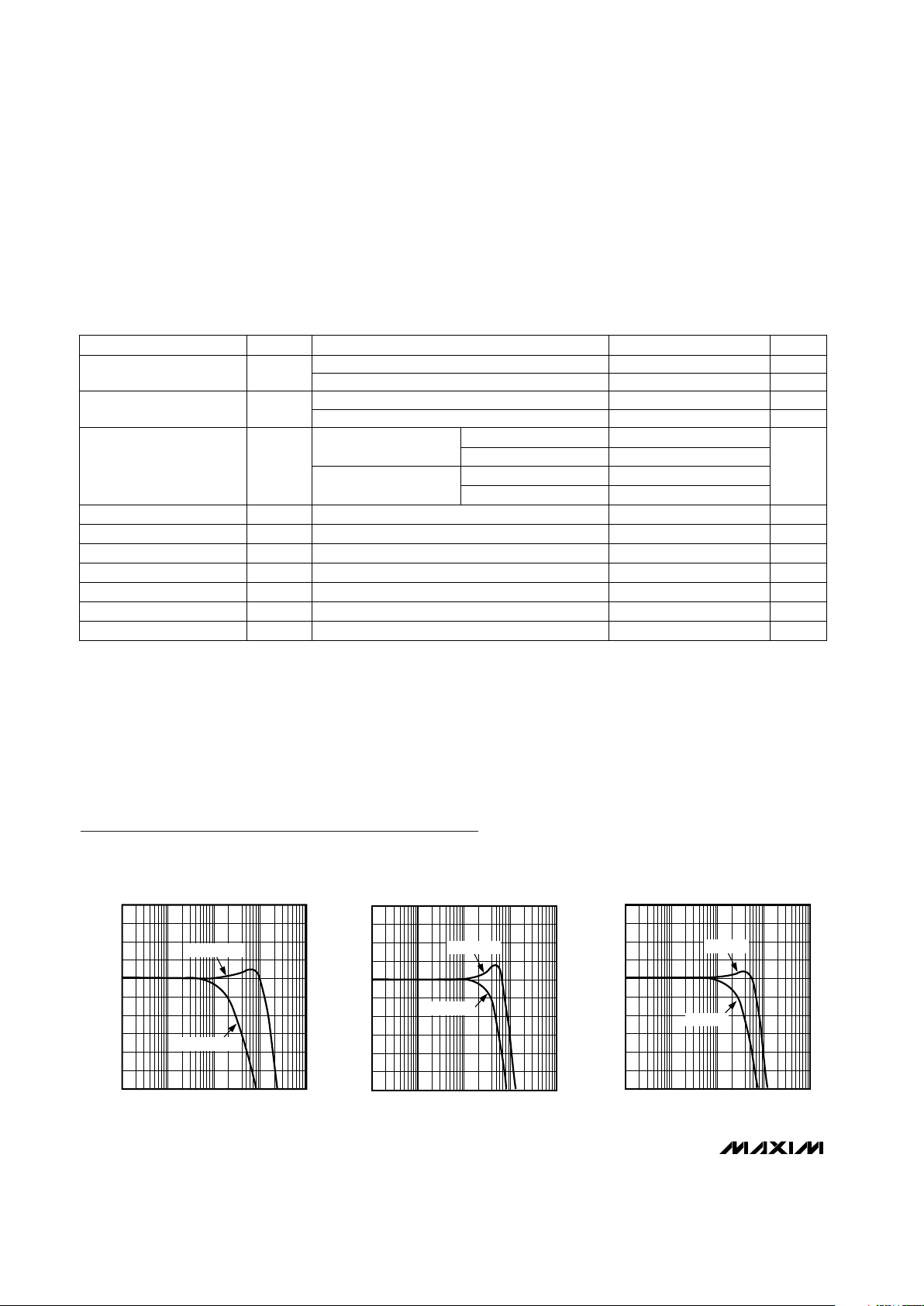
Typical Operating Characteristics
(VCC= +5V, RL = 100kΩ to VCC/ 2, small-signal V
OUT
= 100mVp-p, large-signal V
OUT
= 1Vp-p, TA= +25°C, unless otherwise noted.)
MAX4174/5, MAX4274/5, MAX4281/2/4
SOT23, Rail-to-Rail, Fixed-Gain
GainAmps/Open-Loop Op Amps
4 _______________________________________________________________________________________
Note 1: MAX4174/MAX4175/MAX4281 and MAX4274/MAX4275/MAX4282 and MAX4284 are 100% production tested at
T
A
= +25°C. All temperature limits are guaranteed by design.
Note 2: Guaranteed by design.
Note 3: The input common-mode range for IN_+ is guaranteed by a functional test. A similar test is done on the IN_- input. See the
Applications Information
section for more information on the input voltage range of the GainAmp.
Note 4: For AV= -0.5V/V and AV= -0.25V/V, the output voltage swing is limited by the input voltage range.
Note 5: Includes noise from on-chip resistors.
Note 6: The gain accuracy test is performed with the GainAmp in noninverting configuration. The output voltage swing is limited by
the input voltage range for certain gains and supply voltage conditions. For situations where the output voltage swing is limited by the valid input range, the output limits are adjusted accordingly.
4
-6
1k 100k 1M10k 10M
LARGE-SIGNAL GAIN
vs. FREQUENCY
MAX4174 TOC01
FREQUENCY (Hz)
NORMALIZED GAIN (dB)
-5
-4
-3
-2
-1
0
1
2
3
AV = +2.25V/V
AV = +1.25V/V
4
-6
1k 100k 1M10k 10M
LARGE-SIGNAL GAIN
vs. FREQUENCY
MAX4174 TOC02
FREQUENCY (Hz)
NORMALIZED GAIN (dB)
-5
-4
-3
-2
-1
0
1
2
3
AV = +4V/V
AV = +2.5V/V
4
-6
1k 100k 1M10k 10M
LARGE-SIGNAL GAIN
vs. FREQUENCY
MAX4174 TOC03
FREQUENCY (Hz)
NORMALIZED GAIN (dB)
-5
-4
-3
-2
-1
0
1
2
3
AV = +9V/V
AV = +5V/V
Shorted to V
EE
MHz2
No sustained oscillations, AV= 1V/V
f = 10kHz
VCC= 5V, V
OUT
= 4V step
GBW
RL= 100kΩ
VCC= 5V, V
OUT
= 4V step
µs
VEE+ 0.05V < V
OUT
< V
CC
- 0.1V, RL= 100kΩ
mA
Gain Bandwidth Product
V/µs
RL= 1kΩ
10
CONDITIONS
0.7
7
SRSlew Rate
Settling Time to within 0.01%
Short-Circuit Current
pF470C
LOAD
Capacitive Load Stability
nV/√Hz
60e
n
Input Noise Voltage Density
Shorted to V
CC
mA65
VEE+ 0.25V < V
OUT
< V
CC
- 0.3V, RL= 1kΩ
160 250
dB
60 100
80 100
28
mV
28
VOH/V
OL
Output Voltage Swing
dB
A
VOL
Large-Signal Voltage Gain
90 120
UNITSMIN TYP MAXSYMBOLPARAMETER
ELECTRICAL CHARACTERISTICS—MAX4281/MAX4282/MAX4284 Open-Loop Op Amps
(continued)
(VCC= +2.5V to +5.5V, VEE= 0, V
IN+
= V
IN-
= VCC/ 2, RLto VCC/ 2, RL= open, TA= T
MIN
to T
MAX
, unless otherwise noted. Typical
values are at V
CC
= +5V and TA= +25°C.) (Note 1)
VCC- V
OH
VOL- V
EE
VCC- V
OH
VOL- V
EE
f = 10kHz
fA/√Hz
1.8i
n
Input Noise Current Density
Output settling to 1% ms1Power-Up Time
MAX4174/5, MAX4274/5, MAX4281/2/4
SOT23, Rail-to-Rail, Fixed-Gain
GainAmps/Open-Loop Op Amps
_______________________________________________________________________________________
5
Typical Operating Characteristics (continued)
(VCC= +5V, RL = 100kΩ to VCC/ 2, small-signal V
OUT
= 100mVp-p, large-signal V
OUT
= 1Vp-p, TA= +25°C, unless otherwise noted.)
4
-6
1k 100k 1M10k 10M
LARGE-SIGNAL GAIN
vs. FREQUENCY
MAX4174 TOC04
FREQUENCY (Hz)
NORMALIZED GAIN (dB)
-5
-4
-3
-2
-1
0
1
2
3
AV = +21V/V
AV = +10V/V
4
-6
1k 100k 1M10k 10M
LARGE-SIGNAL GAIN
vs. FREQUENCY
MAX4174 TOC05
FREQUENCY (Hz)
NORMALIZED GAIN (dB)
-5
-4
-3
-2
-1
0
1
2
3
AV = +50V/V
AV = +25V/V
4
-6
1k 100k 1M10k 10M
LARGE-SIGNAL GAIN
vs. FREQUENCY
MAX4174 TOC06
FREQUENCY (Hz)
NORMALIZED GAIN (dB)
-5
-4
-3
-2
-1
0
1
2
3
AV = +100V/V
AV = +51V/V
4
-6
1k 100k 1M10k 10M
SMALL-SIGNAL GAIN
vs. FREQUENCY
MAX4174 TOC07
FREQUENCY (Hz)
NORMALIZED GAIN (dB)
-5
-4
-3
-2
-1
0
1
2
3
AV = +2.25V/V
AV = +1.25V/V
4
-6
1k 100k 1M10k 10M
SMALL-SIGNAL GAIN
vs. FREQUENCY
MAX4174 TOC08
FREQUENCY (Hz)
NORMALIZED GAIN (dB)
-5
-4
-3
-2
-1
0
1
2
3
AV = +4V/V
AV = +2.5V/V
4
-6
1k 100k 1M10k 10M
SMALL-SIGNAL GAIN
vs. FREQUENCY
MAX4174 TOC09
FREQUENCY (Hz)
NORMALIZED GAIN (dB)
-5
-4
-3
-2
-1
0
1
2
3
AV = +9V/V
AV = +5V/V
MAX4174/MAX4175
4
-6
1k 100k 1M10k 10M
SMALL-SIGNAL GAIN
vs. FREQUENCY
MAX4174 TOC10
FREQUENCY (Hz)
NORMALIZED GAIN (dB)
-5
-4
-3
-2
-1
0
1
2
3
AV = +21V/V
AV = +10V/V
4
-6
1k 100k 1M10k 10M
SMALL-SIGNAL GAIN
vs. FREQUENCY
MAX4174 TOC11
FREQUENCY (Hz)
NORMALIZED GAIN (dB)
-5
-4
-3
-2
-1
0
1
2
3
AV = +50V/V
AV = +25V/V
4
-6
1k 100k 1M10k 10M
SMALL-SIGNAL GAIN
vs. FREQUENCY
MAX4174 TOC12
FREQUENCY (Hz)
NORMALIZED GAIN (dB)
-5
-4
-3
-2
-1
0
1
2
3
AV = +100V/V
AV = +51V/V
MAX4174/5, MAX4274/5, MAX4281/2/4
SOT23, Rail-to-Rail, Fixed-Gain
GainAmps/Open-Loop Op Amps
6 _______________________________________________________________________________________
1k 10k 100k 1M
TOTAL HARMONIC DISTORTION
vs. FREQUENCY
MAX4174 TOC13
FREQUENCY (Hz)
THD (dB)
0
-120
-100
-80
-60
-40
-20
AV = +3V/V
AV = +10V/V
V
OUT
= 1Vp-p
AV = +1.25V/V
1k 10k 100k 1M
TOTAL HARMONIC DISTORTION
vs. FREQUENCY
MAX4174 TOC14
FREQUENCY (Hz)
THD (dB)
0
-120
-100
-80
-60
-40
-20
AV = +25V/V
AV = +51V/V
V
OUT
= 1Vp-p
-120
-90
-100
-110
-80
-70
-60
0 2.01.50.5 1.0 2.5 3.0 3.5 4.0 4.5 5.0
TOTAL HARMONIC DISTORTION
vs. OUTPUT VOLTAGE SWING
MAX4174 TOC15
VOLTAGE SWING (Vp-p)
THD (dB)
AV = +1.25V/V
AV = +3V/V
AV = +10V/V
f = 10kHz
Typical Operating Characteristics (continued)
(VCC= +5V, RL = 100kΩ to VCC/ 2, small-signal V
OUT
= 100mVp-p, large-signal V
OUT
= 1Vp-p, TA= +25°C, unless otherwise noted.)
MAX4174/MAX4175
-120
-90
-100
-110
-80
-70
-60
0 2.01.50.5 1.0 2.5 3.0 3.5 4.0 4.5 5.0
TOTAL HARMONIC DISTORTION
vs. OUTPUT VOLTAGE SWING
MAX4174 TOC16
VOLTAGE SWING (Vp-p)
THD (dB)
AV = +25V/V
AV = +51V/V
f = 10kHz
1 10 100 1k 10k 100k
VOLTAGE NOISE DENSITY vs. FREQUENCY
(A
V
= +1.25, +3, +10)
MAX4174/5 toc 17
FREQUENCY (Hz)
1000
10
100
AV = +10V/V
AV = +3V/V
AV = +1.25V/V
VOLTAGE NOISE DENSITY (nV/√Hz)
1 10 100 1k 10k 100k
VOLTAGE NOISE DENSITY vs. FREQUENCY
(A
V
= +25, +51)
MAX4174/5 toc 18
FREQUENCY (Hz)
1000
10
100
AV = +25V/V
AV = +51V/V
VOLTAGE NOISE DENSITY (nV/√Hz)
INCLUDES RESISTOR NOISE
1 10 100 1k 10k 100k
CURRENT NOISE DENSITY vs.
FREQUENCY
MAX4174/5 toc19
FREQUENCY (Hz)
10
1
CURRENT NOISE DENSITY (fA/√Hz)

MAX4174/5, MAX4274/5, MAX4281/2/4
SOT23, Rail-to-Rail, Fixed-Gain
GainAmps/Open-Loop Op Amps
_______________________________________________________________________________________ 7
Typical Operating Characteristics (continued)
(VCC= +5V, RL = 100kΩ to VCC/ 2, small-signal V
OUT
= 100mVp-p, large-signal V
OUT
= 1Vp-p, TA= +25°C, unless otherwise noted.)
2µs/div
C
L
= 0
INPUT
VOLTAGE
A
V
= +1.25V/V
OUTPUT
500mV/div
A
V
= +3V/V
OUTPUT
50mV/div
A
V
= +5V/V
OUTPUT
500mV/div
A
V
= +10V/V
OUTPUT
500mV/div
A
V
= +25V/V
OUTPUT
500mV/div
A
V
= +51V/V
OUTPUT
500mV/div
MAX4174/5 toc 20
LARGE-SIGNAL PULSE RESPONSE
2µs/div
C
L
= 0
INPUT
VOLTAGE
A
V
= +1.25V/V
OUTPUT
50mV/div
A
V
= +3V/V
OUTPUT
50mV/div
A
V
= +5V/V
OUTPUT
50mV/div
A
V
= +10V/V
OUTPUT
50mV/div
A
V
= +25V/V
OUTPUT
50mV/div
A
V
= +51V/V
OUTPUT
50mV/div
MAX4174/5 toc 21
SMALL-SIGNAL PULSE RESPONSE
MAX4174/MAX4175

MAX4174/5, MAX4274/5, MAX4281/2/4
SOT23, Rail-to-Rail, Fixed-Gain
GainAmps/Open-Loop Op Amps
8 _______________________________________________________________________________________
Typical Operating Characteristics (continued)
(VCC= +5V, RL = 100kΩ to VCC/ 2, small-signal V
OUT
= 100mVp-p, large-signal V
OUT
= 1Vp-p, TA= +25°C, unless otherwise noted.)
-200
-100
-150
50
0
-50
150
100
200
-50 -5 10-35 -20 25 40 55 70 85
INPUT OFFSET VOLTAGE vs.
TEMPERATURE
MAX4174/5 toc 25
TEMPERATURE (°C)
INPUT OFFSET VOLTAGE (µV)
VCC = 2.5V
VCC = 5.5V
-200
0
200
400
600
800
1000
-45 -15-30 0 153045607590
INPUT BIAS CURRENT
vs. TEMPERATURE
MAX4174/5 toc 26
TEMPERATURE (°C)
INPUT BIAS CURRENT (pA)
VCC = 2.5V
VCC = 5.5V
240
280
260
320
300
360
340
380
-50 -20 -5-35 10 25 40 55 70 85
SUPPLY CURRENT vs. TEMPERATURE
MAX4174/5 toc 27
TEMPERATURE (°C)
SUPPLY CURRENT (µA)
VCC = 4V
VCC = 2.5V
VCC = 3V
VCC = 5V
VCC = 5.5V
-100
-60
-80
-20
-40
20
0
40
80
60
100
-50 -20 -5 10-35 25 40 55 70 85
VOH AND VOL vs. TEMPERATURE
(V
CC
= 2.5V)
MAX4174/5 toc 28
TEMPERATURE (°C)
VOLTAGE (mV)
VOL, R
L
= 1kΩ
VOL, R
L
= 10kΩ
VOL, R
L
= 100kΩ
VOH, R
L
= 10kΩ
VOH, R
L
= 100kΩ
VOH, R
L
= 1kΩ
-100
-60
-40
-20
-80
40
60
0
20
80
100
160
180
120
140
200
-50 -20 -5 10-35 25 40 55 70 85
VOH AND VOL vs. TEMPERATURE
(V
CC
= 5.5V)
MAX4174/5 toc 29
TEMPERATURE (°C)
VOLTAGE (mV)
VOL, R
L
= 1kΩ
VOL, R
L
= 100kΩ
VOL, R
L
= 100kΩ
VOH, R
L
= 10kΩ
VOH, R
L
= 100kΩ
VOH, R
L
= 1kΩ
MAX4174/MAX4175/MAX4281/MAX4282/MAX4284
-70
100 10k 100k1k 1M
POWER-SUPPLY REJECTION
vs. FREQUENCY
MAX4174 TOC22
FREQUENCY (Hz)
PSR (dB)
-95
-90
-85
-80
-75
100 10k 100k1k 1M
OUTPUT IMPEDANCE
vs. FREQUENCY
MAX4174 TOC23
FREQUENCY (Hz)
OUTPUT IMPEDANCE (Ω)
100
0.01
0.1
1
10
5.0
4.0
1 10 100
OUTPUT VOLTAGE SWING
vs. R
LOAD
MAX4174 TOC24
R
LOAD
(kΩ)
V
SWING
(Vp-p)
4.9
4.8
4.7
4.6
4.5
4.4
4.3
4.2
4.1

MAX4174/5, MAX4274/5, MAX4281/2/4
SOT23, Rail-to-Rail, Fixed-Gain
GainAmps/Open-Loop Op Amps
_______________________________________________________________________________________
9
1 10k 1M10010 1k 100k 10M
OPEN-LOOP GAIN AND PHASE
vs. FREQUENCY
MAX4174/5 toc30
FREQUENCY (Hz)
OPEN-LOOP GAIN (dB)
PHASE (degrees)
140
120
100
80
60
40
0
-20
-40
20
160
-45
-90
-135
-180
-225
-270
-315
0
4
-6
-5
1k 10k 100k 1M 10M
SMALL-SIGNAL GAIN
vs. FREQUENCY
-4
-3
MAX4174/5 toc31
FREQUENCY (Hz)
GAIN (dB)
-2
-1
0
1
2
3
4
-1
-2
-3
-4
-5
-6
1k 10k 100k 1M 10M
LARGE-SIGNAL GAIN
vs. FREQUENCY
0
MAX4174/5 toc32
FREQUENCY (Hz)
GAIN (dB)
1
2
3
0
-50
-60
-70
-80
-90
-100
1k 10k 100k100 1M 10M
COMMON-MODE REJECTION
vs. FREQUENCY
-40
MAX4174/5 toc33
FREQUENCY (Hz)
CMR (dB)
-30
-20
-10
0
-60
-80
-70
-90
-100
-110
-10
-20
-30
-40
-50
-120
1M1k 10k 100k
TOTAL HARMONIC DISTORTION
vs. FREQUENCY
MAX4174/5 toc36
FREQUENCY (Hz)
THD (dB)
AV = 1
V
OUT
= 1Vp-p
1000
100
10
10 100 1k1 10k 100k
VOLTAGE NOISE DENSITY
vs. FREQUENCY
MAX4174/5 toc34
FREQUENCY (Hz)
VOLTAGE NOISE DENSITY (nV/√Hz)
10
1
10 100 1k1 10k 100k
CURRENT NOISE DENSITY
vs. FREQUENCY
MAX4174/5 toc35
FREQUENCY (Hz)
CURRENT NOISE DENSITY (fA/√Hz)
-50
-80
-90
-85
-95
-55
-60
-65
-70
-75
1M 10M1k 10k 100k
MAX4282
CROSSTALK vs. FREQUENCY
MAX4174/5 toc37
FREQUENCY (Hz)
CROSSTALK (dB)
-50
-55
-60
-65
-70
-75
1M 10M1k 10k 100k
MAX4284
CROSSTALK vs. FREQUENCY
MAX4174/5 toc38
FREQUENCY (Hz)
CROSSTALK (dB)
THREE AMPLIFIERS DRIVEN,
ONE OUTPUT MEASURED
Typical Operating Characteristics
(VCC= +5V, RL = 100kΩ to VCC/ 2, small-signal V
OUT
= 100mVp-p, large-signal V
OUT
= 1Vp-p, TA= +25°C, unless otherwise noted.)
MAX4281/MAX4282/MAX4284

MAX4174/5, MAX4274/5, MAX4281/2/4
SOT23, Rail-to-Rail, Fixed-Gain
GainAmps/Open-Loop Op Amps
10 ______________________________________________________________________________________
OUT
IN-
IN+
V
CC
V
EE
R
G
MAX4174
OUT
IN-
IN+
V
CC
V
EE
MAX4281
OUT
IN-
IN+
V
CC
V
CC
V
EE
V
EE
150k
150k
R
B
R
B
R
G
R
F
R
F
MAX4175
Functional Diagrams
Pin Description
16 QSOP14 SO/TSSOP5 SOT23 8 SO
MAX4281
8 SO/µMAX 8 SO/µMAX
MAX4274/
MAX4275
MAX4282
5 SOT23
FUNCTION
MAX4174/
MAX4175
1, 5,
8
—
No Connection.
Not internally
connected.
N.C.8, 9
—
—
75
—
—
Positive SupplyV
CC
44885
24
Inverting Amplifier
Input. Connects to
RGfor MAX4174/
4175/4274/4275.
IN-, INA-,
INB-, INC-,
IND-
2, 6,
11, 15
2, 6,
9, 13
2, 6
33
2, 64
Noninverting
Amplifier Input.
Internally biased to
VCC/ 2 for
MAX4175/MAX4275
IN+, INA+,
INB+, INC+,
IND+
3, 5,
12, 14
3, 5,
10, 12
3, 53, 53
42
Negative Supply or
Ground
V
EE
13114
61
42
Amplifier Output
OUT, OUTA,
OUTB,
OUTC,
OUTD
NAME
1, 7,
10, 16
1, 7,
8, 14
1, 71, 71
MAX4284
NAME FUNCTION
PIN

MAX4174/5, MAX4274/5, MAX4281/2/4
SOT23, Rail-to-Rail, Fixed-Gain
GainAmps/Open-Loop Op Amps
______________________________________________________________________________________ 11
Detailed Description
Maxim’s GainAmp fixed-gain amplifiers combine a lowcost rail-to-rail op amp with internal gain-setting resistors. Factory-trimmed on-chip resistors provide 0.1%
gain accuracy while decreasing design size, cost, and
layout. Three versions are available in this amplifier
family: single/dual/quad open-loop, unity-gain-stable
devices (MAX4281/MAX4282/MAX4284); single/dual
fixed-gain devices (MAX4174/MAX4274); and single/
dual devices with fixed gain plus internal V
CC
/ 2 bias
at the noninverting input (MAX4175/MAX4275). All
amplifiers feature rail-to-rail outputs and drive a 1kΩ
load while maintaining excellent DC accuracy.
Open-Loop Op Amps
The single/dual/quad MAX4281/MAX4282/MAX4284
are high-performance, open-loop op amps with rail-torail outputs. These devices are compensated for unitygain stability, and feature a gain bandwidth (GBW) of
2MHz. The op amps in these ICs feature an input common-mode range that extends from 150mV below the
negative rail to within 1.2V of the positive rail. These
high performance op amps serve as the core for this
family of GainAmp fixed-gain amplifiers. Although the
-3dB bandwidth will not correspond to that of a fixedgain amplifier in higher gain configurations, these
open-loop op-amps can be used to prototype designs.
Internal Gain-Setting Resistors
Maxim’s proprietary laser trimming techniques produce
the necessary RF/RGvalues (Figure 1), so many gain
offerings are easily available. These GainAmp fixed-gain
amplifiers feature a negative-feedback resistor network
that is laser trimmed to provide a gain-setting feedback
ratio (RF/RG) with 0.1% typical accuracy. The standard
op amp pinouts allow the GainAmp fixed-gain amplifiers
to drop in directly to existing board designs, easily
replacing op-amp-plus-resistor gain blocks.
GainAmp Bandwidth
GainAmp fixed-gain amplifiers feature factory-trimmed
precision resistors to provide fixed inverting gains from
-0.25V/V to -100V/V or noninverting gains from
+1.25V/V to +101V/V. The op-amp core is decompensated strategically over the gain-set options to maximize bandwidth. Open-loop decompensation increases
GBW product, ensuring that usable bandwidth is maintained with increasing closed-loop gains. A GainAmp
with a fixed gain of AV= 100V/V has a -3dB bandwidth
of 230kHz. By comparison, a unity-gain-stable op amp
configured for AV= 100V/V would yield a -3dB bandwidth of only 20kHz (Figure 2). Decompensation is performed at five intermediate gain sets, as shown in the
Gain Selection Guide
. Low gain decompensation great-
ly increases usable bandwidth, while decompensation
above gains of +25V/V offers diminished returns.
V
CC
/ 2 Internal Bias
The MAX4175/MAX4275 GainAmp fixed-gain amplifiers
with the V
CC
/ 2 bias option are identical to standard
GainAmp fixed-gain amplifiers, with the added feature
of V
CC
/ 2 internal bias at the noninverting inputs. Two
150kΩ resistors form a voltage-divider for self-biasing
the noninverting input, eliminating external bias resistors for AC-coupled applications, and allowing maximum signal swing at the op amp’s rail-to-rail output for
single-supply systems (see
Typical Operating Circuit
).
For DC-coupled applications, use the MAX4174/
MAX4274.
High-Voltage (±17V) Input Fault Protection
The MAX4174/MAX4175/MAX4274/MAX4275 include
±17V input fault protection. For normal operation, see
the input voltage range specification in the
Electrical
Characteristics
. Overdriven inputs up to ±17V will not
OUT
A
V
=
-R
F
R
G
R
G
R
F
IN-
IN+
V
CC
V
EE
AV = 1 +
R
F
R
G
Figure 1. Internal Gain-Setting Resistors
FREQUENCY (Hz)
GAIN (dB)
60
0
10
20
30
40
-3dB
50
10 10k 100k 1M 10M100 1k
20kHz
230kHz
MAX4281, AV = 100
2MHz GBW
MAX4174,
A
V
= 100
23MHz GBW
Figure 2. Gain-Bandwidth Comparison

MAX4174/5, MAX4274/5, MAX4281/2/4
SOT23, Rail-to-Rail, Fixed-Gain
GainAmps/Open-Loop Op Amps
12 ______________________________________________________________________________________
cause output phase reversal. A back-to-back SCR
structure at the input pins allows either input to safely
swing ±17V relative to VEE(Figure 3). Additionally, the
internal op-amp inputs are diode clamped to either
supply rail for the protection of sensitive input stage circuitry. Current through the clamp diodes is limited by a
5kΩ resistor at the noninverting input, and by RGat the
inverting input. An IN+ or IN- fault voltage as high as
±17V will cause less than 3.5mA of current to flow
through the input pin, protecting both the GainAmp and
the signal source from damage.
Applications Information
GainAmp fixed-gain amplifiers offer a precision, fixed
gain amplifier in a small package that can be used in a
variety of circuit board designs. GainAmp fixed-gain
amplifiers can be used in many op amp circuits that use
resistive negative feedback to set gain, and that do not
require other connections to the op-amp inverting input.
Both inverting and noninverting op-amp configurations
can be implemented easily using a GainAmp.
GainAmp Input Voltage Range
The MAX4174/MAX4175/MAX4274/MAX4275 combine
both an op amp and gain-setting feedback resistors on
the same chip. Because the inverting input pin is actually tied to the RGinput series resistor, the inverting
input voltage range is different from the noninverting
input voltage range. Just as with a discrete design,
care must be taken not to saturate the inputs/output of
the core op amp, to avoid signal distortions or clipping.
The inverting inputs (IN_-) of the MAX4174/MAX4175/
MAX4274/MAX4275 must be within the supply rails or
signal distortion may result. The GainAmp’s inverting
input structure includes diodes to both supplies, such
that driving the inverting input beyond the rails may
cause signal distortions (Figure 1). For applications that
require sensing voltages beyond the rails, use the
MAX4281/MAX4282/MAX4284 open-loop op amps
(Figure 4).
OUT
IN-
IN+
R
G
R
F
5k
V
EE
V
EE
BIAS RESISTORS (MAX4175/MAX4275 ONLY)
NOTE: INPUT STAGE PROTECTION INCLUDES
TWO 17V SCRs AND TWO DIODES AT THE INPUT STAGE.
V
CC
V
CC
V
EE
MAX4174
MAX4175
MAX4274
MAX4275
17V
SCR
V
EE
17V
SCR
Figure 3. Input Protection

MAX4174/5, MAX4274/5, MAX4281/2/4
SOT23, Rail-to-Rail, Fixed-Gain
GainAmps/Open-Loop Op Amps
______________________________________________________________________________________ 13
GainAmp Signal Coupling
and Configurations
Common op-amp configurations include both noninverting and inverting amplifiers. Figures 5–8 show various single and dual-supply circuit configurations.
Single-supply systems benefit from a midsupply bias
on the noninverting input (provided internally on
MAX4175/MAX4275), as this produces a quiescent DC
level at the center of the rail-to-rail output stage signal
swing. For dual-supply systems, ground-referenced
signals may be DC-coupled into the inverting or noninverting inputs.
IN_+ Filter on MAX4175/MAX4275
Internal resistor biasing of the V
CC
/ 2 bias options couples power-supply noise directly to the op amp’s noninverting input. To minimize high-frequency power-supply
noise coupling, add a 1µF to 0.1µF capacitor from IN+
to ground to create a lowpass filter (Figure 6). The lowpass filter resulting from the internal bias resistors and
added capacitor can help eliminate higher frequency
power-supply noise coupling through the noninverting
input.
MAX4281
V
CC
V
CC
R
G
R
F
V
IN
V
OUT
=
-R
F
(V
IN
)
R
G
Figure 4. Single-Supply, DC-Coupled Inverting Amplifier with
Negative Input Voltage
MAX4175
V
CC
R
G
R
B
R
B
R
F
V
IN
0.1µF
V
OUT
=
V
CC
- VIN
(
RF
)
2 R
G
Figure 6. Single-Supply, AC-Coupled Inverting Amplifier
MAX4174
V
EE
V
CC
R
G
R
F
V
IN
V
OUT
= - V
IN
(
RF
)
R
G
Figure 5. Dual-Supply, DC-Coupled Inverting Amplifier
MAX4174
V
EE
V
CC
R
G
R
F
V
IN
V
OUT
= V
IN
(1+
R
F
)
R
G
Figure 7. Dual-Supply, AC-Coupled Noninverting Amplifier

MAX4174/5, MAX4274/5, MAX4281/2/4
SOT23, Rail-to-Rail, Fixed-Gain
GainAmps/Open-Loop Op Amps
14 ______________________________________________________________________________________
MAX4174
V
EE
V
CC
R
G
R
F
R
ISO
C
L
R
L
OUTPUT
INPUT
Figure 9. Dual-Supply, Capacitive-Load Driving Circuit
Figure 10. Small-Signal/Large-Signal Transient Response with
Excessive Capacitive Load with Isolation Resistor
AV = +5V/V
50mV/div
INPUT
OUTPUT
OUTPUT
AV = +5V/V
500mV/div
Supply Bypassing and Board Layout
All devices in the GainAmp family operate from a +2.5V
to +5.5V single supply or from ±1.25V to ±2.75V dual
supplies. For single-supply operation, bypass the
power supply with a 0.1µF capacitor to ground. For
dual supplies, bypass each supply to ground. Bypass
with capacitors as close to the device as possible, to minimize lead inductance and noise. A printed circuit board
with a low-inductance ground plane is recommended.
Capacitive-Load Stability
Driving large capacitive loads can cause instability in
most low-power, rail-to-rail output amplifiers. The fixed-
gain amplifiers of this GainAmp family are stable with
capacitive loads up to 470pF. Stability with higher
capacitive loads can be improved by adding an isolation
resistor in series with the op-amp output, as shown in
Figure 9. This resistor improves the circuit’s phase margin by isolating the load capacitor from the amplifier’s
output. In Figure 10, a 1000pF capacitor is driven with a
100Ω isolation resistor exhibiting some overshoot but no
oscillation. Figures 11 and 12 show the typical small-signal pulse responses of GainAmp fixed-gain amplifiers
with 250pF and 470pF capacitive loads and no isolation
resistor.
MAX4174
V
EE
V
CC
R
G
R
F
V
IN
V
OUT
= V
IN
(1+
R
F
)
R
G
Figure 8. Dual-Supply, DC-Coupled Noninverting Amplifier

MAX4174/5, MAX4274/5, MAX4281/2/4
SOT23, Rail-to-Rail, Fixed-Gain
GainAmps/Open-Loop Op Amps
______________________________________________________________________________________ 15
2µs/div
INPUT
A
V
= +1.25V/V
OUTPUT
50mV/div
A
V
= +3V/V
OUTPUT
50mV/div
A
V
= +5V/V
OUTPUT
50mV/div
A
V
= +10V/V
OUTPUT
50mV/div
A
V
= +25V/V
OUTPUT
50mV/div
A
V
= +51V/V
OUTPUT
50mV/div
Figure 11. MAX4174/MAX4175 Small-Signal Pulse Response
(C
L
= 250pF, RL= 100kΩ)
Figure 12. MAX4174/MAX4175 Small-Signal Pulse Response
(C
L
= 470pF, RL= 100kΩ)
2µs/div
INPUT
A
V
= +1.25V/V
OUTPUT
50mV/div
A
V
= +3V/V
OUTPUT
50mV/div
A
V
= +5V/V
OUTPUT
50mV/div
A
V
= +10V/V
OUTPUT
50mV/div
A
V
= +25V/V
OUTPUT
50mV/div
A
V
= +51V/V
OUTPUT
50mV/div

MAX4174/5, MAX4274/5, MAX4281/2/4
SOT23, Rail-to-Rail, Fixed-Gain
GainAmps/Open-Loop Op Amps
16 ______________________________________________________________________________________
Gain Selection Guide
RF/R
G
INVERTING
GAIN
1+ (RF/RG)
NONINVERTING
GAIN
AB* 0.25 1.25
-3dB BW
(kHz)
†
1700
GAIN
CODE
ACDS
AC 0.5 1.5 1280 ACDT
AD* 1 2 590 ACDU
AE 1.25 2.25 450 ACDV
TOP MARK
ACET
ACEU
ACEV
ACEW
AF 1.5 2.5 1180 ACDW ACEX
AG* 2 3 970 ACDX ACEY
AH 2.5 3.5 820 ACDY ACEZ
AJ 3 4 690 ACDZ ACFA
AK* 4 5 970 ACEA ACFB
AL 5 6 790 ACEB ACFC
AM 6 7 640 ACEC ACFD
AN 8 9 480 ACED ACFE
AO* 9 10 640 ACEE ACFF
BA* 10 11 560 ACEF ACFG
BB 12.5 13.5 460 ACEG ACFH
BC 15 16 390 ACEH ACFI
BD 20 21 300 ACEI ACFJ
BE* 24 25 590 ACEJ ACFK
BF 25 26 580 ACEK ACFL
BG 30 31 510 ACEL ACFM
BH 40 41 390 ACEM ACFN
BJ* 49 50 310 ACEN ACFO
BK* 50 51 330 ACEO ACFP
BL 60 61 310 ACEP ACFQ
BM 80 81 260 ACEQ ACFR
BN* 99 100 230 ACER ACFS
CA* 100 101 230 ACES ACFT
Note: Gains in the noninverting configuration are 1+ (RF/RG) and range from +1.25V/V to +101V/V. For a +1V/V gain, use the
MAX4281/MAX4282/MAX4284.
*
Preferred Gains. These gain versions are available as samples and in small quantities.
†
The -3dB bandwidth is the same for inverting and noninverting configurations.
MAX4174 MAX4175

MAX4174/5, MAX4274/5, MAX4281/2/4
SOT23, Rail-to-Rail, Fixed-Gain
GainAmps/Open-Loop Op Amps
______________________________________________________________________________________ 17
Pin Configurations (continued)
TOP VIEW
SOT23-5
MAX4275
8
7
6
5
1
2
3
4
V
CC
OUTB
INB-
INB+
µMAX/SO
OUTA
INA+
INA-
V
CC
V
CC
R
R
R
R
R
G
R
G
R
F
R
F
V
EE
MAX4175
5
4
1
2
3
OUT
V
CC
V
CC
V
EE
R
R
R
G
R
F
IN+
SOT23-5
MAX4281
5
4
1
2
3
IN-
OUT
V
CC
V
EE
IN+
MAX4274
8
7
6
5
1
2
3
4
V
CC
OUTB
INB-
INB+
µMAX/SO
OUTA
INA+
INA-
R
G
R
G
R
F
R
F
V
EE
MAX4282
8
7
6
5
1
2
3
4
V
CC
OUTB
INB-
INB+
µMAX/SO
SO/TSSOP
QSOP
OUTA
INA+
INA-
V
EE
MAX4284
16
15
14
13
1
2
3
4
OUTD
IND-
IND+
INC+
OUTA
INA+
INA-
V
CC
12
11
10
9
5
6
7
8
V
EE
INC-
OUTC
N.C.
INB+
OUTB
INB-
N.C.
MAX4284
14
13
12
11
1
2
3
4
OUTD
IND-
IND+
INC+
OUTA
INA+
INA-
V
CC
10
9
8
5
6
7
V
EE
INC-
OUTC
INB+
OUTB
INB-
MAX4281
8
7
6
5
1
2
3
4
V
CC
OUT
N.C.
N.C.
SO
N.C.
IN+
IN-
V
EE
-
+
-
+
-
+
-
+
-
+
-
+
+
-
+
-
+
-
+
-
+
-
+
-
+
-
+
-
+
-
+
-
+

MAX4174/5, MAX4274/5, MAX4281/2/4
SOT23, Rail-to-Rail, Fixed-Gain
GainAmps/Open-Loop Op Amps
18 ______________________________________________________________________________________
Ordering Information (continued)
TRANSISTOR COUNTS:
MAX4174: 178
MAX4175: 178
MAX4274: 332
MAX4275: 332
MAX4281: 178
MAX4282: 332
MAX4284: 328
SUBSTRATE CONNECTED TO V
EE
Selector Guide
Note: Refer to Gain Selection Guide for SOT top marks.
*
Insert the desired gain code (from the Gain Selection Guide) in
the blank to complete the part number. Refer to Gain Selection
Guide for a list of preferred gains.
Chip Information
INVERTING GAINS
AVAILABLE (V/V)
(INVERTING, RF/RG)
NONINVERTING
GAIN
(V/V)
MAX4174_ -0.25 to -100 +1.25 to +101
INTERNAL
RESISTORS
Yes
INTERNAL
VCC/2 BIAS
PART*
No
NO. OF
AMPS PER
PACKAGE
1
PIN-PACKAGE
5-pin SOT23
MAX4175_ -0.25 to -100 +1.25 to +101 Yes Yes 1 5-pin SOT23
MAX4274_ -0.25 to -100 +1.25 to +101 Yes No 2 8-pin µMAX/SO
MAX4275_ -0.25 to -100 +1.25 to +101 Yes Yes 2 8-pin µMAX/SO
MAX4281_
Open Loop,
Unity-Gain Stable
No No 1
5-pin SOT23,
8-pin SO
MAX4282_
Open Loop,
Unity-Gain Stable
No No 2 8-pin µMAX/SO
MAX4284_
Open Loop,
Unity-Gain Stable
No No 4
14-pin SO/TSSOP,
16-pin QSOP
PART*
MAX4281EUK-T
-40°C to +85°C
MAX4274_EUA
-40°C to +85°C
5 SOT23-5
MAX4281ESA
TEMP. RANGE
PIN-
PACKAGE
-40°C to +85°C 8 SO
8 µMAX
MAX4274_ESA
MAX4284EUD
-40°C to +85°C
MAX4282EUA
-40°C to +85°C
-40°C to +85°C 8 SO
14 TSSOP
MAX4284EEE -40°C to +85°C 16 QSOP
8 µMAX
MAX4282ESA -40°C to +85°C 8 SO
MAX4275_EUA
-40°C to +85°C 8 µMAX
MAX4275_ESA -40°C to +85°C 8 SO
ACDR
TOP
MARK
—
—
—
—
—
—
—
—
—
*
Insert the desired gain code (from the Gain Selection Guide) in the blank to complete the part number.
MAX4284ESD -40°C to +85°C 14 SO —

MAX4174/5, MAX4274/5, MAX4281/2/4
SOT23, Rail-to-Rail, Fixed-Gain
GainAmps/Open-Loop Op Amps
______________________________________________________________________________________ 19
SOT5L.EPS
Package Information

MAX4174/5, MAX4274/5, MAX4281/2/4
SOT23, Rail-to-Rail, Fixed-Gain
GainAmps/Open-Loop Op Amps
Maxim cannot assume responsibility for use of any circuitry other than circuitry entirely embodied in a Maxim product. No circuit patent licenses are
implied. Maxim reserves the right to change the circuitry and specifications without notice at any time.
20
____________________Maxim Integrated Products, 120 San Gabriel Drive, Sunnyvale, CA 94086 408-737-7600
© 1999 Maxim Integrated Products Printed USA is a registered trademark of Maxim Integrated Products.
8LUMAXD.EPS
Package Information
 Loading...