19-1184; Rev 0; 12/96
Low-Cost, Precision, High-Side
Current-Sense Amplifier
_______________General Description
The MAX4172 is a low-cost, precision, high-side currentsense amplifier for portable PCs, telephones, and other
systems where battery/DC power-line monitoring is critical. High-side power-line monitoring is especially useful in
battery-powered systems, since it does not interfere with
the battery charger’s ground path. Wide bandwidth
and ground-sensing capability make the MAX4172
suitable for closed-loop battery-charger and generalpurpose current-source applications. The 0V to 32V input
common-mode range is independent of the supply voltage, which ensures that current-sense feedback remains
viable, even when connected to a battery in deep discharge.
To provide a high level of flexibility, the MAX4172 functions with an external sense resistor to set the range of
load current to be monitored. It has a current output that
can be converted to a ground-referred voltage with a single resistor, accommodating a wide range of battery voltages and currents.
An open-collector power-good output (PG) indicates
when the supply voltage reaches an adequate level to
guarantee proper operation of the current-sense amplifier. The MAX4172 operates with a 3.0V to 32V supply
voltage, and is available in a space-saving, 8-pin µMAX
or SO package.
____________________________Features
♦ Low-Cost, High-Side Current-Sense Amplifier
♦ ±0.5% Typical Full-Scale Accuracy Over
Temperature
♦ 3V to 32V Supply Operation
♦ 0V to 32V Input Range—Independent of
Supply Voltage
♦ 800kHz Bandwidth [V
200kHz Bandwidth [V
SENSE
SENSE
= 100mV (1C)]
= 6.25mV (C/16)]
♦ Available in Space-Saving µMAX and SO
Packages
______________Ordering Information
PART
MAX4172ESA
MAX4172EUA -40°C to +85°C
*
Contact factory for availability.
TEMP. RANGE PIN-PACKAGE
-40°C to +85°C
8 SO
8 µMAX*
MAX4172
________________________Applications
Portable PCs: Notebooks/Subnotebooks/Palmtops
Battery-Powered/Portable Equipment
Closed-Loop Battery Chargers/Current Sources
Smart-Battery Packs
Portable/Cellular Phones
Portable Test/Measurement Systems
Energy Management Systems
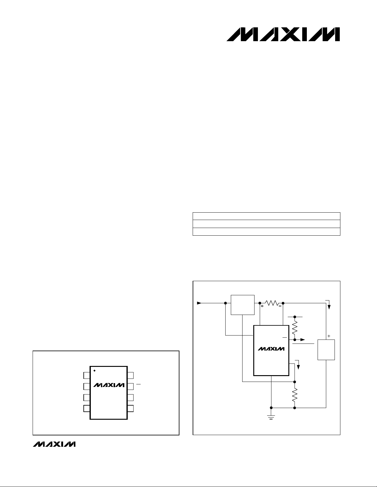
__________________Pin Configuration
TOP VIEW
1
RS+
2
RSN.C.
N.C.
________________________________________________________________
MAX4172
3
4
µMAX/SO
8
V+
PG
7
OUT
6
5
GND
__________Typical Operating Circuit
UNREGULATED
DC SUPPLY
3V TO 32V
LOW-COST
SWITCHING
REGULATOR
FEEDBACK LOOP
V
OUT
LOW-COST BATTERY CHARGER/CURRENT SOURCE
R
SENSE
RS+
V+
MAX4172
= 500mV/A
50mΩ
V
SENSE
GND
RS-
PG
OUT
0V TO 32V
ANALOG OR
LOGIC SUPPLY
100k
POWER GOOD
I
V
R
OUT
1k
Maxim Integrated Products
OUT
SENSE
=
/ 100Ω
LOAD/
BATTERY
2A
1
For free samples & the latest literature: http://www.maxim-ic.com, or phone 1-800-998-8800

Low-Cost, Precision, High-Side
Current-Sense Amplifier
ABSOLUTE MAXIMUM RATINGS
V+, RS+, RS-, PG ...................................................-0.3V to +36V
OUT..............................................................-0.3V to (V+ + 0.3V)
Differential Input Voltage, V
Current into Any Pin..........................................................±50mA
Continuous Power Dissipation (T
SO (derate 5.88mW/°C above +70°C)..........................471mW
µMAX (derate 4.10mW/°C above +70°C) .....................330mW
Stresses beyond those listed under “Absolute Maximum Ratings” may cause permanent damage to the device. These are stress ratings only, and functional
MAX4172
operation of the device at these or any other conditions beyond those indicated in the operational sections of the specifications is not implied. Exposure to
absolute maximum rating conditions for extended periods may affect device reliability.
RS+
- V
............................±700mV
RS-
= +70°C)
A
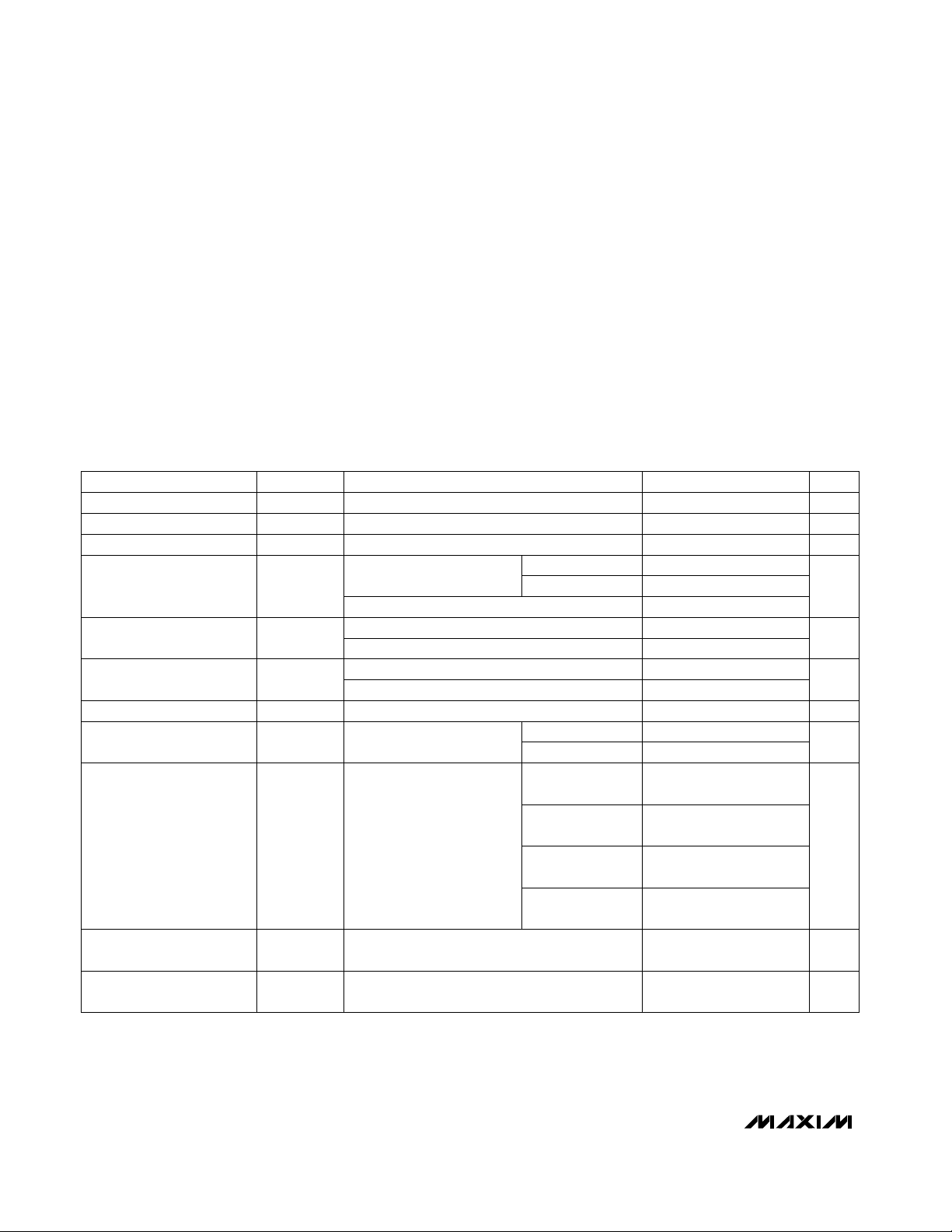
ELECTRICAL CHARACTERISTICS
(V+ = +3V to +32V; RS+, RS- = 0V to 32V; TA= T
= +25°C.)
T
A
Input Voltage Range
Supply Current
Input Offset Voltage mVMAX4172EUA ±0.2 ±1.6
Positive Input Bias Current
Negative Input Bias Current
Voltage
SENSE
Low-Level Current Error
OUT Power-Supply
Rejection Ratio
OUT Common-Mode
Rejection Ratio
OUT
OUT
V
I
RS+
I
RS-
V+
OS
RS-
/ ∆V+
/ ∆V
RS+
to T
MIN
= 0mA
I
OUT
V+ = 12V, V
V
≤ 2.0V
RS+
V
> 2.0V, I
RS+
V
≤ 2.0V, I
RS+
V
> 2.0V
RS+
V
≤ 2.0V
RS+
V
SENSE
V
= 12V (Note 1)
RS+
V
SENSE
V
= 12V
RS+
3V ≤ V+ ≤ 32V, V
2.0V < V
; unless otherwise noted. Typical values are at V+ = +12V, RS+ = 12V,
MAX
RS+
OUT
OUT
= 6.25mV, V+ = 12V,
= 100mV, V+ = 12V,
< 32V
RS+
Operating Temperature Range
MAX4172E_A....................................................-40°C to +85°C
Storage Temperature Range.............................-65°C to +150°C
Lead Temperature (soldering, 10sec).............................+300°C
CONDITIONS
= 12V
= 0mA
= 0mA
RS+
> 2.0V
MAX4172ESA
-325 42.5
-650 85
MAX4172ESA
MAX4172EUA ±15
MAX4172ESA,
TA= -40°C to 0°C
MAX4172EUA,
TA= -40°C to 0°C
MAX4172ESA,
TA= 0°C to +85°C
MAX4172EUA,
TA= 0°C to +85°C
TA= 0°C to +85°C
±0.1 ±0.75
4
0 27 42.5
05085
UNITSMIN TYP MAXSYMBOLPARAMETER
±8.0
±20
±50
±10
±15
V332V+Operating Voltage Range
V032V
mA0.8 1.6I
µA
µA
mV150 175Maximum V
µA
µAOutput Current Error
µA/V0.2∆I
µA/V0.03∆I
2 _______________________________________________________________________________________

Low-Cost, Precision, High-Side
Current-Sense Amplifier
ELECTRICAL CHARACTERISTICS (continued)
(V+ = +3V to +32V; RS+, RS- = 0V to 32V; TA= T
= +25°C.)
T
A
Maximum Output Voltage
(OUT)
Bandwidth
Maximum Output Current
Transconductance
OUT
G
m
V+ Threshold for PG Output
Low (Note 2)
PG Output Low Voltage
OL
Leakage Current into PG
Power-Off Input Leakage
Current (RS+, RS-)
OUT Settling Time to 1%
Note 1: 6.25mV = 1/16 of typical full-scale sense voltage (C/16).
Note 2: Valid operation of the MAX4172 is guaranteed by design when PG is low.
to T
MIN
; unless otherwise noted. Typical values are at V+ = +12V, RS+ = 12V,
MAX
CONDITIONS
I
≤ 1.5mA
OUT
V
= 100mV
SENSE
V
= 6.25mV (Note 1)
SENSE
Gm= I
V
SENSE
/ (V
OUT
RS+
= 100mV, V
- V
RS+
RS-
),
> 2.0V
TA= 0°C to +85°C
TA= -40°C to 0°C
V+ rising
V+ falling 2.67
I
= 1.2mA, V+ = 2.9V, TA= +25°C
SINK
V+ = 2.5V, TA= +25°C
V+ = 0V, V
V
SENSE
V
SENSE
V
SENSE
V
SENSE
= V
RS+
= 32V µA0.1 1
RS-
= 0mV to 100mV, 10% to 90%
= 100mV to 0mV, 90% to 10% ns800OUT Fall Time
= 5mV to 100mV
Rising
Falling
= 150mV MΩ20OUT Output Resistance
800
200
9.8 10 10.2
9.7 10 10.3
2.77
1.3
6
MAX4172
UNITSMIN TYP MAXSYMBOLPARAMETER
VV+ - 1.2
kHz
mA1.5 1.75I
mA/V
V
V0.4V
µA1
ns400OUT Rise Time
µs
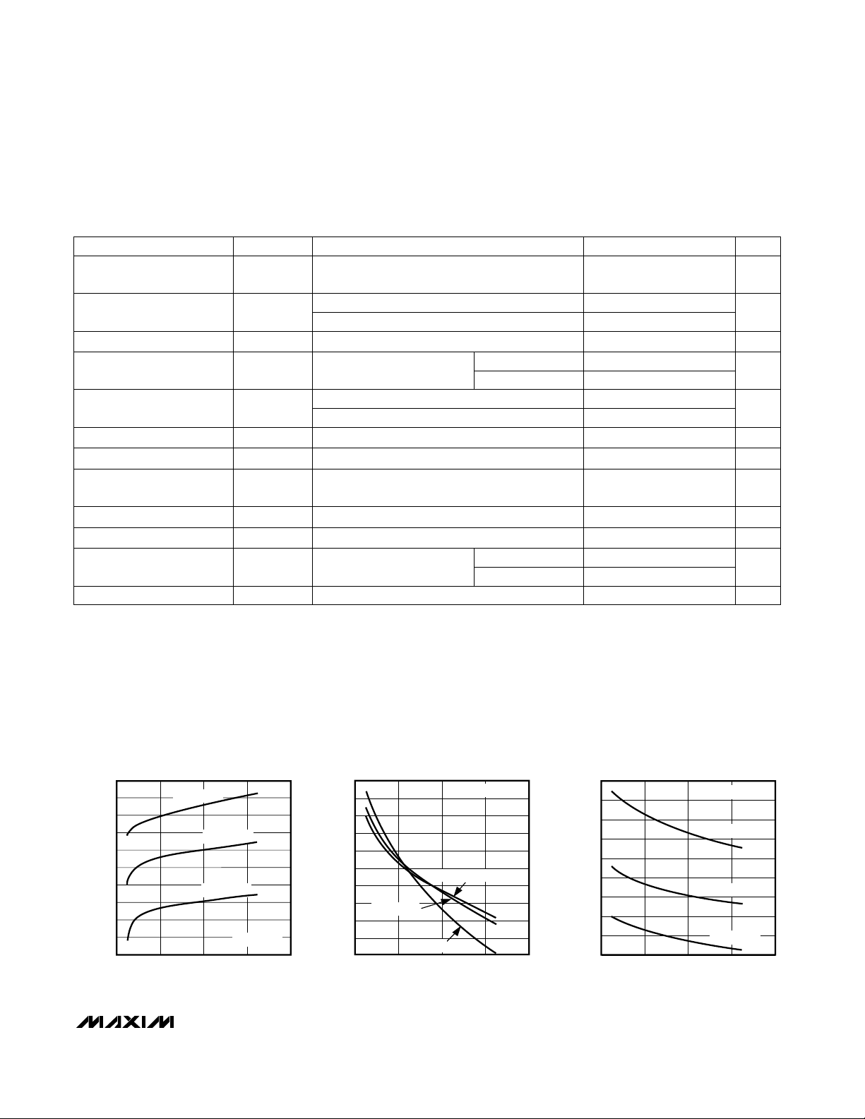
__________________________________________Typical Operating Characteristics
(V+ = +12V, V
1000
950
900
850
800
750
700
650
SUPPLY CURRENT (µA)
600
550
500
010
= 12V, R
RS+
SUPPLY CURRENT
vs. SUPPLY VOLTAGE
TA = +85°C
20
V+ (V)
= 1kΩ, TA= +25°C, unless otherwise noted.)
OUT
vs. SUPPLY VOLTAGE
0.5
0.4
MAX4172-01
0.3
TA = +25°C
TA = -40°C
I
OUT
30
= 0mA
40
0.2
0.1
0
ERROR (%)
-0.1
-0.2
-0.3
-0.4
-0.5
010
TA = +25°C
OUTPUT ERROR
V
SENSE
TA = +85°C
TA = -40°C
20 30
V+ (V)
= 100mV
40
MAX4172-03
1.5
1.0
0.5
0
-0.5
-1.0
ERROR (%)
-1.5
-2.0
-2.5
-3.0
010
C/16 LOAD OUTPUT ERROR
vs. SUPPLY VOLTAGE
20
V+ (V)
_______________________________________________________________________________________ 3
V
SENSE
TA = -40°C
TA = +25°C
TA = +85°C
= 6.25mV
30
MAX4172-02
40
 Loading...