

Page 1
1
19-1224; Rev 3; 1/07
High-Output-Drive, Precision, Low-Power, Single-
Supply, Rail-to-Rail I/O Op Amps with Shutdown
General Description
The MAX4165–MAX4169 family of operational amplifiers
combines excellent DC accuracy with high output current
drive, single-supply operation, and rail-to-rail inputs and
outputs. These devices operate from a single +2.7V to
+6.5V supply, or from dual ±1.35V to ±3.25V supplies.
They typically draw 1.2mA supply current, and are guaranteed to deliver 80mA output current.
The MAX4166/MAX4168 have a shutdown mode that
reduces supply current to 38µA per amplifier and
places the outputs into a high-impedance state. The
MAX4165–MAX4169’s precision performance combined with high output current, wide input/output
dynamic range, single-supply operation, and low power
consumption makes them ideal for portable audio
applications and other low-voltage, battery-powered
systems. The MAX4165 is available in the space-saving
5-pin SOT23 package and the MAX4166 is available in
a tiny 2mm x 2mm x 0.8mm µDFN package.
Selector Guide
PART
MAX4165 Single —
MAX4166 Single Yes
MAX4167 Dual —
MAX4168 Dual Yes
MAX4169 Quad —
AMPS PER
PACKAGE
SHUTDOWN
MODE
Applications
Portable/Battery-Powered Audio Applications
Portable Headphone Speaker Drivers
Laptop/Notebook Computers
Sound Ports/Cards
Set-Top Boxes
Cell Phones
Hands-Free Car Phones (kits)
Signal Conditioning
Digital-to-Analog Converter Buffers
Transformer/Line Drivers
Motor Drivers
Features
♦ 80mA (min) Output Drive Capability
♦ Rail-to-Rail Input Common-Mode Voltage Range
♦ Rail-to-Rail Output Voltage Swing
♦ 1.2mA Supply Current per Amplifier
♦ +2.7V to +6.5V Single-Supply Operation
♦ 5MHz Gain-Bandwidth Product
♦ 250µV Offset Voltage
♦ 120dB Voltage Gain (R
♦ 88dB Power-Supply Rejection Ratio
♦ No Phase Reversal for Overdriven Inputs
♦ Unity-Gain Stable for Capacitive Loads to 250pF
♦ Low-Power Shutdown Mode:
Reduces Supply Current to 38µA Places
Outputs in High-Impedance State
♦ Available in 5-Pin SOT23 Package (MAX4165) or
2mm x 2mm x 0.8mm µDFN (MAX4166)
= 100kΩΩ)
L
Ordering Information
PART TEMP RANGE
MAX4165EUK-T -40°C to +85°C 5 SOT23-5 AABY
MAX4166EPA -40°C to +85°C 8 Plastic DIP —
MAX4166ESA -40°C to +85°C 8 SO —
MAX4166EUA -40°C to +85°C 8 µMAX —
MAX4166ELA+T -40°C to +85°C 8 µDFN-8 AAG
+
Denotes lead-free package.
Ordering Information continued on last page.
PINPACKAGE
TOP
MARK
Pin Configurations
TOP VIEW
OUT
V
IN+
1
MAX4165
2
EE
3
5
V
CC
IN-
4
MAX4165–MAX4169
Typical Operating Circuit appears at end of data sheet.
SOT23-5
Pin Configurations continued at end of data sheet.
________________________________________________________________
Maxim Integrated Products
For pricing, delivery, and ordering information, please contact Maxim/Dallas Direct! at
1-888-629-4642, or visit Maxim’s website at www.maxim-ic.com.
1
Page 2
High-Output-Drive, Precision, Low-Power, SingleSupply, Rail-to-Rail I/O Op Amps with Shutdown
ABSOLUTE MAXIMUM RATINGS
Supply Voltage (VCCto VEE)....................................................7V
IN_+, IN_-, SHDN_............................(V
OUT_ (shutdown mode) ...................(V
Output Short-Circuit Duration to V
Continuous Power Dissipation (T
5-Pin SOT23 (derate 7.10mW/°C above +70°C)..........571mW
8-Pin Plastic DIP (derate 9.09mW/°C above +70°C) ...727mW
8-Pin SO (derate 5.88mW/°C above +70°C)................471mW
8-Pin µMAX (derate 4.10mW/°C above +70°C) ...........330mW
Note 1: Continuous power dissipation should also be observed.
Stresses beyond those listed under “Absolute Maximum Ratings” may cause permanent damage to the device. These are stress ratings only, and functional
operation of the device at these or any other conditions beyond those indicated in the operational sections of the specifications is not implied. Exposure to
absolute maximum rating conditions for extended periods may affect device reliability.
CC
A
- 0.3V) + (VCC+ 0.3V)
EE
- 0.3V) + (VCC+ 0.3V)
EE
or VEE(Note 1) .....Continuous
= +70°C)
DC ELECTRICAL CHARACTERISTICS
(VCC= +2.7V to +6.5V, VEE= 0V, VCM= 0V, V
MAX4165–MAX4169
noted.)
PARAMETER SYMBOL CONDITIONS MIN TYP MAX UNITS
Input Offset Voltage V
Input Bias Current I
Input Offset Current I
Differential Input Resistance R
Common-Mode Input
Voltage Range
Common-Mode
Rejection Ratio
OS
B
OS
IN(DIFF)
V
CM
CMRR
Power-Supply Rejection Ratio PSRR V
Output Resistance R
Off-Leakage Current
in Shutdown
Large-Signal Voltage Gain A
OUT
I
OUT(SHDN) VSHDN
VOL
= (VCC/ 2), RL= 100kΩ to (VCC/ 2), V
OUT
V
= V
to V
EE
CC
= V
to V
EE
CC
= V
to V
EE
CC
+ - VIN- | 1.8V
≤
+ - VIN- | > 1.8V
V
V
| V
| V
CM
CM
CM
IN
IN
Inferred from CMRR test V
- 0.25V <
V
EE
< (V
V
A
CM
CC
VCL
+ 0.25V)
CC
= 2.7V to 6.5V
= +1V/V 0.1
< 0.8V, V
V
V
= 5V
CC
V
OUT
OUT
8-Pin µDFN (derate 4.8mW/°C above +70°C) .............380mW
10-Pin µMAX (derate 5.60mW/°C above +70°C) ..........444mW
14-Pin Plastic DIP (derate 10.00mW/°C above +70°C) 800mW
14-Pin SO (derate 8.33mW/°C above +70°C)...............667mW
Operating Temperature Range ...........................-40°C to +85°C
Junction Temperature......................................................+150°C
Storage Temperature Range .............................-65°C to +150°C
Lead Temperature (soldering, 10s) .................................+300°C
≥ 2V, TA= +25°C, unless otherwise
SHDN
MAX416_EPA/EPD
MAX416_ESA/ESD
MAX416_EUA/EUB/ELA
MAX416_EUK
MAX4169E_D
0.25 0.85
0.25 0.85
0.35 1.7
0.35 1.5
0.25 1.0
±50 ±150 nA
±1 ±15 nA
500
2
- 0.25 V
EE
MAX416_EPA/EPD
MAX416_ESA/ESD
MAX416_EUA/EUB/ELA
MAX416_EUK
MAX4169E_D
MAX416_EPA/EP
D 72 88
MAX416_ESA/ESD
MAX416_EUA/EUB/ELA
MAX416_EUK
MAX4169E_D
= 0V to V
OUT
CC
= 0.2V to 4.8V, RL = 100k 95 120
= 0.6V to 4.4V, RL = 25 71 83
Ω
72 93
72 93
62 89
63 90
71 93
72 88
72 86
72 86
70 88
Ω
±0.001 ±2 μA
+ 0.25 V
CC
mV
kΩ
dB
dB
kΩ
dB
2 _______________________________________________________________________________________
Page 3
High-Output-Drive, Precision, Low-Power, Single-
Supply, Rail-to-Rail I/O Op Amps with Shutdown
DC ELECTRICAL CHARACTERISTICS (continued)
(V
CC
= +2.7V to +6.5V, V
EE
= 0V, V
CM
= 0V, V
OUT
= (V
CC
/ 2), R
L
= 100kΩ to (V
CC
/ 2), V
SHDN
≥ 2V, T
A
= +25°C, unless otherwise
noted.)
PARAMETER SYMBOL CONDITIONS MIN TYP MAX UNITS
R
L
= 100kΩ
V
CC
- V
OH
15 30
mVOutput Voltage Swing V
OUT
V
CC
= 5V
V
OL
- V
EE
10 25
R
L
= 25Ω
V
CC
- V
OH
340 430
V
OL
- V
EE
160 350
Output Source/Sink Current
(Note 2)
V
OUT
= 0.6V to (V
CC
- 0.6V) ±80 ±125 mA
SHDN Logic Threshold
V
IL
Shutdown mode 0.8
V
(Note 3)
V
IH
Normal mode 2.0
SHDN Input Bias Current
V
EE
< V
SHDN
< V
CC
±3.0 µA
Operating Supply-Voltage
Range
V
CC
Inferred from PSRR test 2.7 6.5 V
Quiescent Supply Current
I
CC
V
CC
= 5V 1.3 1.5
mA
(per Amplifier)
V
CC
= 3V 1.2 1.4
Shutdown Supply Current
V
SHDN
< 0.8V
V
CC
= 5V 58 75
µA
(per Amplifier)
I
CC(SHDN)
V
CC
= 3V 38 49
DC ELECTRICAL CHARACTERISTICS
(V
CC
= +2.7V to +6.5V, V
EE
= 0V, V
CM
= 0V, V
OUT
= (V
CC
/ 2), R
L
= 100kΩ to (V
CC
/ 2), V
SHDN
≥ 2V, T
A
= -40°C to +85°C, unless
otherwise noted.) (Note 4)
PARAMETER SYMBOL CONDITIONS MIN TYP MAX UNITS
MAX416_EPA/EPD 1.0
mV
MAX416_ESA/ESD 1.0
Input Offset Voltage V
OS
V
CM
= V
EE
to V
CC
4.9
MAX416_EUK 4.3
MAX4169E_D 1.2
Offset-Voltage Tempco ΔVOS/ΔT ±3 µV/°C
Input Bias Current I
B
V
CM
= V
EE
to V
CC
±225 nA
Input Offset Current I
OS
V
CM
= V
EE
to V
CC
±21 nA
Common-Mode Input
Voltage Range
V
CM
Inferred from CMRR test V
EE
- 0.15 V
CC
+ 0.15 V
MAX416_EPA/EPD
71
dB
Common-Mode
Rejection Ratio
CMRR
V
EE
- 0.15V < V
CM
<
(V
CC
+ 0.15V)
MAX416_ESA/ESD
71
56
MAX416_EUK
57
MAX4169E_D
69
MAX416_EPA/EPD
67
dB
MAX416_ESA/ESD
67
Power-Supply Rejection Ratio PSRR V
CC
= 2.7V to 6.5V
65
MAX416_EUK
65
MAX4169E_D
66
MAX4165–MAX4169
_______________________________________________________________________________________ 3
MAX416_EUA/EUB /ELA
MAX416_EUA/EUB /ELA
MAX416_EUA/EUB /EL
A
Page 4
High-Output-Drive, Precision, Low-Power, SingleSupply, Rail-to-Rail I/O Op Amps with Shutdown
DC ELECTRICAL CHARACTERISTICS (continued)
(VCC= +2.7V to +6.5V, VEE= 0V, VCM= 0V, V
otherwise noted.)
Off-Leakage Current
in Shutdown
Large-Signal Voltage Gain
Output Voltage Swing VCC= 5V
I
OUT(SHDN)
A
VOL
V
OUT
Output Source/Sink Current
(Note 2)
V
SHDN Logic Threshold
(Note 3)
SHDN Input Bias Current
MAX4165–MAX4169
Operating Supply-Voltage
Range
Quiescent Supply Current
(per Amplifier)
Shutdown Supply Current
(per Amplifier)
IL
V
IH
CC
I
CC
I
CC(SHDN)
Note 2: Although the minimum output current is guaranteed to be ±80mA, exercise caution to ensure that the absolute maximum
power-dissipation rating of the package is not exceeded.
Note 3: SHDN logic thresholds are referenced to V
Note 4: The MAX4165EUK is 100% tested at +25°C. All temperature limits are guaranteed by design.
= (VCC/ 2), R
OUT
= 100kΩ to (V
L
CC
/ 2), V
CONDITIONS
V
< 0.8V, V
SHDN
VCC= 5V
V
= 0.6V to (VCC- 0.6V) mA±80
OUT
= 0V to V
OUT
V
= 0.2V to 4.8V, R
OUT
V
= 0.6V to 4.4V, R
OUT
R
= 100kΩ
L
R
= 25Ω
L
CC
L
L
VCC- V
VOL- V
VCC- V
VOL- V
Shutdown mode
Normal mode
VEE< V
SHDN
< V
CC
Inferred from PSRR test
VCC= 5V
VCC= 3V
V
SHDN
EE
< 0.8V
.
VCC= 5V
VCC= 3V
SHDN
= 100kΩ
= 25Ω
OH
EE
OH
EE
≥ 2V, T
90
66
2.0
= -40°C to +85°C, unless
A
40
30
490
400
0.8
1.7
1.6
82
54
UNITSMIN TYP MAXSYMBOLPARAMETER
µA±5
dB
mV
V
µA±3.5
V2.7 6.5V
mA
µA
AC ELECTRICAL CHARACTERISTICS
(VCC= +2.7V to +6.5V, VEE= 0V, VCM= 0V, V
otherwise noted.)
FPBWFull-Power Bandwidth
Slew Rate SR V/µs
PMPhase Margin 68
Gain Margin GM dB
THDTotal Harmonic Distortion
Settling Time to 0.01% t
Input Capacitance 3
Input Voltage-Noise Density 26
Input Current-Noise Density 0.4
S
IN
e
n
i
n
Channel-to-Channel Isolation
Capacitive Load Stability
Shutdown Time
Enable Time from Shutdown
Power-Up Time t
t
SHDN
t
ENABLE
ON
4 _______________________________________________________________________________________
= (VCC/ 2), R
OUT
= 2.5kΩ to (V
L
CC
/ 2), V
SHDN
≥ 2V, C
= 15pF, TA= +25°C, unless
L
CONDITIONS
V
= 4Vp-p, VCC= 5V
OUT
260
2
21
f = 10kHz, V
A
= +1V/V, 2V step µs
VCL
OUT
= 2Vp-p, A
= +1V/V %
VCL
0.005
2.1
f = 1kHz
f = 1kHz
f = 1kHz, R
A
VCL
= 100kΩ (MAX4167–MAX4169)
L
125
= +1V/V, no sustained oscillations pF250
UNITSMIN TYP MAXSYMBOLPARAMETER
degrees
nV/√Hz
pA/√Hz
MHz5GBWPGain-Bandwidth Product
kHz
pFC
dB
µs1
µs1
µs5
Page 5
MAX4165–MAX4169
High-Output-Drive, Precision, Low-Power, Single-
Supply, Rail-to-Rail I/O Op Amps with Shutdown
_______________________________________________________________________________________
5
70
-30
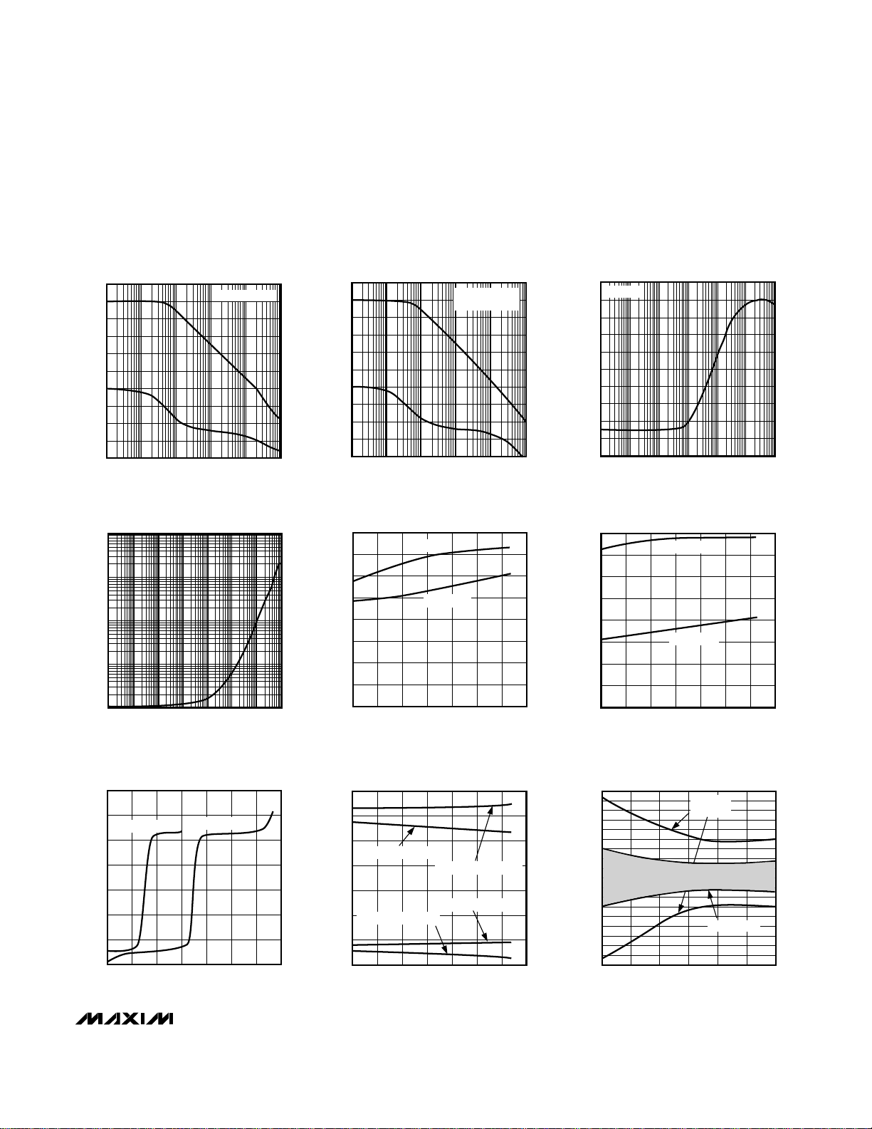
100 1k 10k 100k 1M 10M
GAIN AND PHASE vs. FREQUENCY
10
0
-10
-20
MAX4165-01
FREQUENCY (Hz)
GAIN (dB)
30
20
50
40
60
216
-144
0
-36
-72
-108
72
36
144
108
180
PHASE (DEGREES)
A
VCL
= +1000V/V
70
-30
100 1k 10k 100k 1M 10M
GAIN AND PHASE vs. FREQUENCY
(C
L
= 250pF)
-20
MAX4165-02
FREQUENCY (Hz)
GAIN (dB)
10
0
-10
50
40
30
20
60
216
-144
-108
0
-36
-72
144
108
72
36
180
PHASE (DEGREES)
A
VCL
= +1000V/V
C
L
= 250pF
10
-90
100 1k 10k 100k 1M 10M 100M
POWER-SUPPLY REJECTION RATIO
vs. FREQUENCY
-70
-80
MAX4165-03A
FREQUENCY (Hz)
PSRR (dB)
-50
-60
-30
-40
-10
-20
0
A
VCL
= +1
1000
0.1
1 10 100 1k 10k
100k
1M 10M
OUTPUT IMPEDANCE vs. FREQUENCY
1
MAX4165-03B
FREQUENCY (Hz)
OUTPUT IMPEDANCE (Ω)
10
100
80
-60
0 7
INPUT BIAS CURRENT
vs. COMMON-MODE VOLTAGE
-40
60
MAX4165-06
COMMON-MODE VOLTAGE (V)
INPUT BIAS CURRENT (nA)
1 2 3 4 5 6
40
20
0
-20
VCC = +6.5V
VCC = +2.7V
1.6
0
-40 100
SUPPLY CURRENT PER AMPLIFIER
vs. TEMPERATURE
0.2
1.4
MAX4165-04
TEMPERATURE (°C)
SUPPLY CURRENT (mA)
-20 0 20 40 60 80
1.2
1.0
0.8
0.6
0.4
VCC = +6.5V
VCC = +2.7V
80
0
-40 100
SHUTDOWN SUPPLY CURRENT
PER AMPLIFIER vs. TEMPERATURE
20
10
70
60
MAX4165-05
TEMPERATURE (°C)
SUPPLY CURRENT (µA)
-20 0 20 40 60 80
50
40
30
VCC = +6.5V
VCC = +2.7V
80
-60
-40 100
INPUT BIAS CURRENT
vs. TEMPERATURE
-40
60
MAX4165-07
TEMPERATURE (°C)
INPUT BIAS CURRENT (nA)
-20 0 20 40 60 80
40
20
0
-20
VCC = +6.5V, VCM = V
CC
VCC = +2.7V, VCM = V
CC
VCC = +2.7V, VCM = V
EE
VCC = +6.5V, VCM = V
EE
2.25
-2.25
-40 80
INPUT OFFSET VOLTAGE
vs. TEMPERATURE
-1.75
1.75
1.25
MAX4165-08
TEMPERATURE (°C)
VOLTAGE (mV)
-20
0 20 40 60
0.75
0.25
-0.75
-0.25
-1.25
SOT23-5
PACKAGE
SO PACKAGE
__________________________________________Typical Operating Characteristics
(VCC= +5.0V, VEE= 0V, R
L
= 100kΩ, T
A
= +25°C, unless otherwise noted.)
Page 6
MAX4165–MAX4169
High-Output-Drive, Precision, Low-Power, SingleSupply, Rail-to-Rail I/O Op Amps with Shutdown
6 _______________________________________________________________________________________
____________________________Typical Operating Characteristics (continued)
(VCC= +5.0V, VEE= 0V, R
L
= 100kΩ, T
A
= +25°C, unless otherwise noted.)
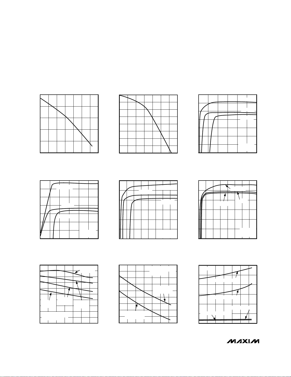
2.00
1.75
-40 100
MINIMUM OPERATING VOLTAGE
vs. TEMPERATURE
1.80
1.95
MAX4165-09
TEMPERATURE (°C)
MINIMUM OPERATING VOLTAGE (V)
-20 0 20 40 60 80
1.90
1.85
88.0
84.0
84.5
-40 100
COMMON-MODE REJECTION RATIO
vs. TEMPERATURE
85.5
85.0
87.5
87.0
MAX4165-10
TEMPERATURE (°C)
CMRR (dB)
-20 0 20 40 60 80
86.5
86.0
140
0
20
0 0.6
LARGE-SIGNAL GAIN vs. OUTPUT VOLTAGE
(SINKING, V
CC
= 6.5V)
60
40
120
MAX4165-11
OUTPUT VOLTAGE (V)
LARGE-SIGNAL GAIN (dB)
0.1
0.2
0.3
0.4 0.5
100
80
RL = 100kΩ
RL = 1kΩ
RL = 100Ω
VCC = +6.5V
R
L
to V
CC
125
90
95
0 0.6
LARGE-SIGNAL GAIN vs. OUTPUT VOLTAGE
(SOURCING, V
CC
= 6.5V)
105
100
120
MAX4165-12
OUTPUT VOLTAGE (V)
LARGE-SIGNAL GAIN (dB)
0.1 0.2 0.3 0.4 0.5
115
110
RL = 100kΩ
RL = 1kΩ
RL = 100Ω
VCC = +6.5V
R
L
to V
EE
125
107
109
-40 100
LARGE-SIGNAL GAIN vs. TEMPERATURE
(R
L
= 100kΩ)
111
123
MAX4165-15a
TEMPERATURE (°C)
LARGE-SIGNAL GAIN (dB)
-20
0 20 40 60 80
121
119
117
115
113
VCC = +6.5V
R
L
to V
CC
or V
EE
VCC = +2.7V
R
L
to V
CC
or V
EE
V
OUTp-p
= VCC - 1V
R
L
= 100kΩ
110
60
65
-40 100
LARGE-SIGNAL GAIN vs. TEMPERATURE
(R
L
= 100Ω)
75
70
105
MAX4165-15
TEMPERATURE (°C)
LARGE-SIGNAL GAIN (dB)
-20
0 20 40 60 80
100
95
90
85
80
VCC = +2.7V
R
L
to V
EE
VCC = +2.7V
R
L
to V
CC
VCC = +6.5V
R
L
to V
CC
V
OUTp-p
= VCC - 1V
R
L
= 100Ω
VCC = +6.5V
R
L
to V
EE
120
0
20
0 0.40
LARGE-SIGNAL GAIN vs. OUTPUT VOLTAGE
(SINKING, V
CC
= 2.7V)
40
100
MAX4165-13
OUTPUT VOLTAGE (V)
LARGE-SIGNAL GAIN (dB)
0.05 0.10 0.15 0.20 0.25 0.30 0.35
80
60
RL = 100kΩ
RL = 100Ω
RL = 1kΩ
VCC = +2.7V
R
L
to V
CC
120
0
0 0.40
LARGE-SIGNAL GAIN vs. OUTPUT VOLTAGE
(SOURCING, V
CC
= 2.7V)
40
20
100
MAX4165-14
OUTPUT VOLTAGE (V)
LARGE-SIGNAL GAIN (dB)
0.05
0.15
0.10 0.20
0.25
0.30 0.36
80
60
VCC = +2.7V
R
L
to V
EE
RL = 100kΩ
RL = 100Ω
RL = 1kΩ
120
0
20
-40 100
OUTPUT VOLTAGE LOW
vs. TEMPERATURE
40
100
MAX4165-16
TEMPERATURE (°C)
V
OUT
- V
EE
(mV)
-20
0 20 40 60 80
80
60
VCC = +6.5V, RL = 100Ω
RL to V
CC
VCC = +2.7V, RL = 100Ω
VCC = +6.5V, RL = 100kΩ
VCC = +2.7V, RL = 100kΩ
Page 7

MAX4165–MAX4169
High-Output-Drive, Precision, Low-Power, Single-
Supply, Rail-to-Rail I/O Op Amps with Shutdown
_______________________________________________________________________________________ 7
0.05
0
10 1k100 10k 100k
TOTAL HARMONIC DISTORTION
AND NOISE vs. FREQUENCY
0.01
MAX4165-18
FREQUENCY (Hz)
THD + NOISE (%)
0.02
0.03
0.04
V
OUT
= 2Vp-p
500kHz LOWPASS FILTER
R
L
= 10kΩ TO VCC / 2
1
0.001
4.0
4.6
4.8 5.0
TOTAL HARMONIC DISTORTION AND NOISE
vs. PEAK-TO-PEAK OUTPUT VOLTAGE
0.01
0.1
MAX4165-19
PEAK-TO-PEAK OUTPUT (V)
THD + NOISE (%)
4.2 4.4
RL = 250Ω
RL = 2kΩ
RL = 100kΩ
RL = 25Ω
f = 10kHz
R
L
to VCC / 2
IN
(50mV/div)
OUT
(50mV/div)
SMALL-SIGNAL TRANSIENT RESPONSE
(NONINVERTING)
MAX4165-20
TIME (500ns/div)
A
VCL
= +1V/V
130
80
1k 100k 1M10k 10M
CHANNEL-TO-CHANNEL ISOLATION
vs. FREQUENCY
90
85
MAX4165-19a
FREQUENCY (Hz)
CHANNEL-TO-CHANNEL ISOLATION (dB)
100
95
110
105
120
125
115
IN
(50mV/div)
OUT
(50mV/div)
SMALL-SIGNAL TRANSIENT RESPONSE
(INVERTING)
MAX4165-21
TIME (500ns/div)
A
VCL
= -1V/V
IN
(2V/div)
OUT
(2V/div)
LARGE-SIGNAL TRANSIENT RESPONSE
(NONINVERTING)
MAX4165-22
TIME (5µs/div)
A
VCL
= +1V/V
IN
(2V/div)
OUT
(2V/div)
LARGE-SIGNAL TRANSIENT RESPONSE
(INVERTING)
MAX4165-23
TIME (5µs/div)
A
VCL
= -1V/V
300
0
50
-40 100
OUTPUT VOLTAGE HIGH
vs. TEMPERATURE
250
MAX4165-17
TEMPERATURE (°C)
OUTPUT VOLTAGE HIGH
(mV)
-20 0 20 40 60 80
200
150
100
VCC = +6.5V, RL = 100Ω
VCC = +2.7V, RL = 100Ω
VCC = +6.5V OR + 2.7V, RL = 100kΩ
RL to V
EE
____________________________Typical Operating Characteristics (continued)
(VCC= +5.0V, VEE= 0V, R
L
= 100kΩ, T
A
= +25°C, unless otherwise noted.)
Page 8

MAX4165-MAX4169
High-Output-Drive, Precision, Low-Power, SingleSupply, Rail-to-Rail I/O Op Amps with Shutdown
8 _______________________________________________________________________________________
Pin Description
PIN
MAX4166 MAX4168
MAX4165
1 6 4 — — — — OUT Output
— 1, 5 2, 6 —
— — — 1, 7 1, 13 1, 9 1, 7 OUT1, OUT2 Outputs for Amplifiers 1 and 2
2 4 3 4 4 4 11 V
3 3 1 — — — — IN+ Noninverting Input
— — — 2, 6 2, 12 2, 8 2, 6 IN1-, IN2- Inverting Inputs for Amplifiers 1 and 2
4 2 7 — — — — IN- Inverting Input
— — — 3, 5 3, 11 3, 7 3, 5 IN1+, IN2+ Noninverting Inputs for Amplifiers 1 and 2
5 7 5 8 14 10 4 VCC Positive Supply
— — — — 6, 9 5, 6 —
— 8 8 — — — — SHDN
— — — — — — 8, 14 OUT3, OUT4 Outputs for Amplifiers 3 and 4
— — — — — — 9, 13 IN3-, IN4- Inverting Inputs for Amplifiers 3 and 4
— — — — — — 10, 12 IN3+, IN4+ Noninverting Inputs for Amplifiers 3 and 4
DIP/SO
(MAX
(DFN
MAX4167
DIP/SO (MAX
5, 7, 8,
10
MAX4169
— — N.C. No Connection. Not internally connected.
NAME FUNCTION
EE
SHDN1,
SHDN2
Negative Supply. Ground for singlesupply operation.
Active-Low Shutdown Inputs for
Amplifiers 1 and 2. Drive low for
shutdown mode. Drive high or connect to
V
for normal operation.
CC
Active-Low Shutdown Input. Drive low for
shutdown mode. Drive high or connect to
for normal operation.
V
CC
Page 9

MAX4165–MAX4169
High-Output-Drive, Precision, Low-Power, Single-
Supply, Rail-to-Rail I/O Op Amps with Shutdown
_______________________________________________________________________________________ 9
Applications Information
Package Power Dissipation
Warning: Due to the high output current drive, this op
amp can exceed the absolute maximum power-dissipation rating. As a general rule, as long as the peak cur-
rent is less than or equal to 80mA, the maximum package
power dissipation will not be exceeded for any of the
package types offered. There are some exceptions to this
rule, however. The absolute maximum power-dissipation
rating of each package should always be verified using
the following equations. The following equation gives an
approximation of the package power dissipation:
where: V
RMS
= the RMS voltage from VCCto V
OUT
when sourcing current
= the RMS voltage from V
OUT
to V
EE
when sinking current
I
RMS
= the RMS current flowing out of or into
the op amp and the load
θ = the phase difference between the
voltage and the current. For resistive
loads, COS θ = 1.
For example, the circuit in Figure 1 has a package
power dissipation of 157mW.
Therefore, P
IC(DISS)
= V
RMSIRMS
COS θ
= 157mW
Adding a coupling capacitor improves the package
power dissipation because there is no DC current to
the load, as shown in Figure 2.
Therefore, P
IC(DISS)
= V
RMSIRMS
COS θ
= 38.6mW
The absolute maximum power-dissipation rating of this
package would be exceeded if the configuration in
Figure 1 were used with all four of the MAX4169ESD’s
amplifiers at a high ambient temperature of +75°C
(157mW x 4 amplifiers = 628mW + a derating of
8.33mW/°C x 5°C = 669mW). Note that 669mW just
exceeds the absolute maximum power dissipation of
667mW for the 14-pin SO package (see the
Absolute
Maximum Ratings
section).
V V V
I +
I
2
RMS CC DC
RMS
PEAK
≅ −
( )
−
= − − =
≅ = +
=
. .
.
.
. /
.
V
V V
V
V
I A
V
mA
PEAK
RMS
DC
2
6 5 3 25
1 5
2
2 189
0
1 5 60
2
17 67
Ω
V V V
I +
I
2
RMS CC DC
RMS
PEAK
≅ −
( )
−
= − − =
≅ = +
=
. .
.
.
.
. /
.
V
V V
V
V
I
V V
mA
PEAK
RMS
DC
RMS
2
6 5 3 25
1 5
2
2 189
3 25
60
1 5 60
2
71 84
Ω
Ω
P V I COS
IC DISS RMS RMS
( )
≅ θ
6.5V
V
IN
= 3Vp-p
R
C
60Ω
R
MAX4165
MAX4166
Figure 1. A Circuit Example where the MAX4165/MAX4166 is
Being Used in Single-Supply Operation
6.5V
V
IN
= 3Vp-p
R
60Ω
R
C
C
C
CC = 1
2π R
L fL
MAX4165
MAX4166
Figure 2. A Circuit Example where Adding a Coupling
Capacitor Greatly Reduces the Power Dissipation of Its
Package
Page 10

High-Output-Drive, Precision, Low-Power, SingleSupply, Rail-to-Rail I/O Op Amps with Shutdown
INPUT
0.25Vp-p
0.1µF
100k
4.7k
V
= +3V
CC
4.7k
100k
1µF
100k
100k
100k
100k
V
CC
1/2 MAX4167
1/2 MAX4168
= +3V
V
CC
1/2 MAX4167
1/2 MAX4168
900k
47Ω
0.1µF
= +3V
MAX4165–MAX4169
Figure 3. Dual MAX4167/MAX4168 Bridge Amplifier for
200mW at 3V
Single-Supply Speaker Driver
The MAX4165/MAX4166 can be used as a single-supply speaker driver, as shown in the
Circuit
. Capacitor C1 is used for blocking DC (a 0.1µF
ceramic capacitor can be used). When choosing resistors R3 and R4, take into consideration the input bias
current as well as how much supply current can be tolerated. Choose resistors R1 and R2 according to the
amount of gain and current desired. Capacitor C3
ensures unity gain for DC. A 10µF electrolytic capacitor
is suitable for most applications. The coupling capacitor C2 sets a low-frequency pole and is fairly large in
value. For a 32Ω load, a 100µF coupling capacitor
gives a low-frequency pole at 50Hz. The low-frequency
pole can be set according to the following equation:
ƒ = 1 / 2π (R
The circuit shown in Figure 3 uses a dual MAX4167/
MAX4168 to implement a 3V, 200mW amplifier suitable
for use in size-constrained applications. This configuration eliminates the need for the large coupling capacitor required by the single op-amp speaker driver when
single-supply operation is a must. Voltage gain is set to
+10V/V; however, it can be changed by adjusting the
900kΩ resistor value. DC voltage at the speaker is limited to 10mV. The 47Ω and 0.1µF capacitors across the
speaker maintain a low impedance at the load as frequency increases.
Typical Operating
C2)
L
Bridge Amplifier
MAX4165
MAX4166
MAX4167
MAX4168
MAX4169
R3
R3 = R1 R2
32Ω
R1 R2
Figure 4. Reducing Offset Error Due to Bias Current
(Noninverting)
MAX4165
MAX4166
MAX4167
MAX4168
MAX4169
R3
R3 = R1 R2
R1 R2
Figure 5. Reducing Offset Error Due to Bias Current (Inverting)
Rail-to-Rail Input Stage
Devices in the MAX4165–MAX4169 family of high-output-current amplifiers have rail-to-rail input and output
stages designed for low-voltage, single-supply operation. The input stage consists of separate NPN and
PNP differential stages that combine to provide an
input common-mode range that extends 0.25V beyond
the supply rails. The PNP stage is active for input voltages close to the negative rail, and the NPN stage is
active for input voltages near the positive rail. The
switchover transition region, which occurs near VCC/ 2,
has been extended to minimize the slight degradation
in common-mode rejection ratio caused by mismatch of
the input pairs.
10 ______________________________________________________________________________________
Page 11

High-Output-Drive, Precision, Low-Power, Single-
Supply, Rail-to-Rail I/O Op Amps with Shutdown
1kΩ
1kΩ
Figure 6. Input Protection Circuit
Since the input stage switches between the NPN and
PNP pairs, the input bias current changes polarity as the
input voltage passes through the transition region. Match
the effective impedance seen by each input to reduce the
offset error caused by input bias currents flowing through
external source impedances (Figures 4 and 5).
High source impedances, together with input capacitance, can create a parasitic pole that produces an
underdamped signal response. Reducing the input
impedance or placing a small (2pF to 10pF) capacitor
across the feedback resistor improves response.
The MAX4165–MAX4169’s inputs are protected from large
differential input voltages by 1kΩ series resistors and
back-to-back triple diodes across the inputs (Figure 6).
For differential voltages less than 1.8V, input resistance is
typically 500kΩ. For differential input voltages greater
than 1.8V, input resistance is approximately 2kΩ. The
input bias current is given by the following equation:
I
BIAS
= (V
- 1.8V) / 2kΩ
DIFF
Rail-to-Rail Output Stage
The minimum output is within millivolts of ground for
single-supply operation, where the load is referenced
to ground (VEE). Figure 7 shows the input voltage range
and the output voltage swing of a MAX4165 connected
as a voltage follower. The maximum output voltage
swing is load dependent; however, it is guaranteed to
be within 430mV of the positive rail (VCC= 5V) even
with maximum load (25Ω to ground).
Figure 7. Rail-to-Rail Input/Output Range
The MAX4165–MAX4169 have a high tolerance for
capacitive loads. They are stable with capacitive loads
up to 250pF. Figure 8 is a graph of the stable operating
region for various capacitive loads vs. resistive loads.
Figures 9 and 10 show the transient response with
excessive capacitive loads (1500pF), with and without
the addition of an isolation resistor in series with the
output. Figure 11 shows a typical noninverting capacitive-load-driving circuit in the unity-gain configuration.
The resistor improves the circuit’s phase margin by isolating the load capacitor from the op amp’s output.
(1V/div)
OUT
(1V/div)
IN
VCC = +3.0V
= 100kΩ
R
L
MAX4165-fig07
TIME (5µs/div)
Driving Capacitive Loads
MAX4165–MAX4169
______________________________________________________________________________________ 11
Page 12

High-Output-Drive, Precision, Low-Power, SingleSupply, Rail-to-Rail I/O Op Amps with Shutdown
1300
V
1200
1100
1000
CAPACITIVE LOAD (pF)
300
to V
/ 2
R
L
CC
900
UNSTABLE REGION
800
700
600
500
400
200
100
0
10 100k
100 1k 10k
STABLE REGION
RESISTIVE LOAD (kΩ)
= +5.0V
CC
MAX4165-fig08
(20mV/div)
(20mV/div)
VCC = +3.0V, CL = 1500pF
= 100kΩ, R
R
L
IN
OUT
= 0Ω
ISO
TIME (1µs/div)
MAX4165-fig09
Figure 8. Capacitive-Load Stability
MAX4165–MAX4169
VCC = +3.0V, CL = 1500pF
= 100kΩ, R
R
L
IN
(20mV/div)
OUT
(20mV/div)
Figure 10. Small-Signal Transient Response with Excessive
Capacitive Load with Isolation Resistor
Power-Up and Shutdown Modes
The MAX4166/MAX4168 have a shutdown option.
When the shutdown pin (SHDN) is pulled low, supply
current drops to 58µA per amplifier (VCC= +5V), the
amplifiers are disabled, and their outputs are placed in
a high-impedance state. Pulling SHDN high or leaving it
floating enables the amplifier. In the dual MAX4168, the
two amplifiers shut down independently. Figures 12
and 13 show the MAX4166’s output voltage and supply-current responses to a shutdown pulse. The
MAX4166–MAX4169 typically settle within 5µs after
power-up (Figure 14).
= 39Ω
ISO
TIME (1µs/div)
MAX4165-fig10
Figure 9. Small-Signal Transient Response with Excessive
Capacitive Load
R
ISO
C
L
Figure 11. Capacitive-Load-Driving Circuit
Power Supplies and Layout
The MAX4165–MAX4169 can operate from a single
+2.7V to +6.5V supply, or from dual ±1.35V to
±3.25V supplies. For single-supply operation, bypass
the power supply with a 0.1µF ceramic capacitor in
parallel with at least 1µF. For dual-supply operation,
bypass each supply to ground. Good layout improves
performance by decreasing the amount of stray capacitance at the op amps’ inputs and outputs. Decrease
stray capacitance by placing external components
close to the op amps’ pins, minimizing trace and lead
lengths.
12 ______________________________________________________________________________________
Page 13

MAX4165–MAX4169
High-Output-Drive, Precision, Low-Power, Single-
Supply, Rail-to-Rail I/O Op Amps with Shutdown
______________________________________________________________________________________ 13
SHDN
(1V/div)
OUT
(1V/div)
MAX4165-fig12
TIME (5µs/div)
Figure 12. Shutdown Output Voltage Enable/Disable
SHDN
(1V/div)
I
CC
(1mA/div)
MAX4165-fig13
TIME (50µs/div)
Figure 13. Shutdown Enable/Disable Supply Current
V
CC
(1V/div)
OUT
(2V/div)
MAX4165-fig14
TIME (5µs/div)
Figure 14. Power-Up/Down Output Voltage
V
CC
(1V/div)
I
EE
(1mA/div)
MAX4165-fig15
TIME (5µs/div)
Figure 15. Power-Up/Down Supply Current
Page 14

MAX4165–MAX4169
14 ______________________________________________________________________________________
High-Output-Drive, Precision, Low-Power, SingleSupply, Rail-to-Rail I/O Op Amps with Shutdown
Pin Configurations (continued)
TOP VIEW
N.C.
IN-
IN+
V
1
2
MAX4166
3
4
EE
8 7 SHDN
V
CC
6
OUT
5
N.C.
DIP/SO/μMAX
OUT1
IN1-
IN1+
N.C.
SHDN1
1
2
3
4
EE
MAX4168
5
6
7
14
13
12
11
10
9
8
V
OUT2
IN2-
IN2+V
N.C.
SHDN2
N.C.N.C.
IN+
1
N.C. IN-
2
MAX4166
3
V
EE
4
OUT
μDFN
(2mm x 2mm x 0.8mm)
1
OUT1
2
IN1-
IN1+
EE
3
4
5
MAX4168
μMAX
CC
10
1
8
SHDN
7
6
N.C.
5
V
CC
OUT1
IN1-
IN1+
V
2
MAX4167
3
4
EE
8 7 V
6
5
CC
OUT2
IN2-
IN2+
DIP/SO
V
CC
9
OUT2
IN2-
8
7
IN2+V
6
SHDN2SHDN1
OUT1
IN1-
IN1+
V
IN2+
IN2-
CC
1
2
3
4
5
6
7
MAX4169
14
13
12
11
10
OUT4
IN4-
IN4+
V
EE
IN3+
9
IN3-
OUT3OUT2
8
DIP/SO
DIP/SO
Page 15

MAX4165-MAX4169
High-Output-Drive, Precision, Low-Power, Single-
Supply, Rail-to-Rail I/O Op Amps with Shutdown
______________________________________________________________________________________
15
Package Information
(The package drawing(s) in this data sheet may not reflect the most current specifications. For the latest package outline information
go to www.maxim-ic.com/packages
.)
Typical Operating Circuit Ordering Information (continued)
V
CC
R3
C1
V
IN
R4
MAX4165
MAX4166
C2
PART TEMP RANGE
MAX4167EPA
-40°C to +85°C 8 Plastic DIP —
MAX4167ESA -40°C to +85°C 8 SO —
MAX4168EPD
-40°C to +85°C 14 Plastic DIP —
MAX4168ESD -40°C to +85°C 14 SO —
MAX4168EUB -40°C to +85°C 10 μMAX —
MAX4169EPD
-40°C to +85°C 14 Plastic DIP —
PIN-
PACKAGE
MAX4169ESD -40°C to +85°C 14 SO —
R2
32Ω
R1
___________________Chip Information
MAX4165 TRANSISTOR COUNT: 230
MAX4166 TRANSISTOR COUNT: 230
C3
MAX4167 TRANSISTOR COUNT: 462
MAX4168 TRANSISTOR COUNT: 462
MAX4169 TRANSISTOR COUNT: 924
TOP
MARK
8
1
TOP VIEW
Ø0.50±0.1
D
E H
4X S
BOTTOM VIEW
8
1
DIM
A
A1
A2
b
c
D
e
E
H
L
α
S
INCHES
MIN
-
0.002
0.030
0.010
0.005
0.116
0.0256 BSC
0.116
0.188
0.016
0°
0.0207 BSC
MAX
0.043
0.006
0.037
0.014
0.007
0.120
0.120
0.198
0.026
6°
MILLIMETERS
MAX
MIN
-1.10
0.05 0.15
0.950.75
0.25 0.36
0.13 0.18
2.95 3.05
0.65 BSC
2.95 3.05
5.03
4.78
0.66
0.41
6°0°
0.5250 BSC
8LUMAXD.EPS
0.6±0.1
0.6±0.1
A2
e
FRONT VIEW
A1
A
c
b
L
SIDE VIEW
α
PROPRIETARY INFORMATION
TITLE:
PACKAGE OUTLINE, 8L uMAX/uSOP
21-0036
REV.DOCUMENT CONTROL NO.APPROVAL
1
J
1
Page 16

16 ______________________________________________________________________________________
MAX4165-MAX4169
High-Output-Drive, Precision, Low-Power, SingleSupply, Rail-to-Rail I/O Op Amps with Shutdown
Package Information (continued)
(The package drawing(s) in this data sheet may not reflect the most current specifications. For the latest package outline information
go to www.maxim-ic.com/packages
.)
SOT-23 5L .EPS
0.6±0.1
PACKAGE OUTLINE, SOT-23, 5L
21-0057
e
10
Ø0.50±0.1
1
0.6±0.1
TOP VIEW
D2
A2
D1
FRONT VIEW
4X S
H
BOTTOM VIEW
GAGE PLANE
A
b
α
A1
10
1
E2
E1
L
L1
INCHES
DIM
MIN
-A
0.002
A1
A2 0.030 0.037 0.75 0.95
0.116
D1
0.114
D2
0.116
E1
E2
0.114
H
0.187
L
0.0157
L1
0.037 REF
0.007
b
e
0.0197 BSC
0.0035
c
0.0196 REF
S
α
0° 0° 6°
c
MAX
0.043
0.006
0.120
0.118
0.120
0.118
0.199
0.0275
0.0106
0.0078
6°
MILLIMETERS
MIN
-
0.05
2.95
2.89
2.95
2.89
4.75
0.40
0.940 REF
0.177
0.500 BSC
0.090
0.498 REF
SIDE VIEW
PROPRIETARY INFORMATION
TITLE:
PACKAGE OUTLINE, 10L uMAX/uSOP
21-0061
MAX
1.10
0.15
3.05
3.00
3.05
3.00
5.05
0.70
0.270
0.200
REV.DOCUMENT CONTROL NO.APPROVAL
E
1
1
1
1
10LUMAX.EPS
Page 17

MAX4165-MAX4169
High-Output-Drive, Precision, Low-Power, Single-
Supply, Rail-to-Rail I/O Op Amps with Shutdown
Maxim cannot assume responsibility for use of any circuitry other than circuitry entirely embodied in a Maxim product. No circuit patent licenses are
implied. Maxim reserves the right to change the circuitry and specifications without notice at any time.
Maxim Integrated Products, 120 San Gabriel Drive, Sunnyvale, CA 94086 408-737-7600 ____________________
17
© 2007 Maxim Integrated Products is a registered trademark of Maxim Integrated Products, Inc.
Package Information (continued)
(The package drawing(s) in this data sheet may not reflect the most current specifications. For the latest package outline information
go to www.maxim-ic.com/packages
.)
-DRAWING NOT TO SCALE-
D
XXXX
XXXX
XXXX
PIN 1
INDEX AREA
SAMPLE
MARKING
7
A1
A
E
b
A
A2
L
L
e
C
L
e
EVEN TERMINAL
b
A A
(N/2 -1) x e)
PACKAGE OUTLINE,
6, 8, 10L uDFN, 2x2x0.80 mm
21-0164
N
1
C
L
e
ODD TERMINAL
SOLDER
MASK
COVERAGE
PIN 1
0.10x45∞
L1
L
1
A
2
6, 8, 10L UDFN.EPS
COMMON DIMENSIONS
SYMBOL MIN. NOM.
A
0.70 0.75
A1
0.15 0.20 0.25
A2
0.020 0.025 0.035
D 1.95 2.00
1.95 2.00
E
L
0.30 0.40
L1
PACKAGE VARIATIONS
PKG. CODE N e b
-DRAWING NOT TO SCALE-
6L622-1 0.65 BSC 0.30±0.05
0.10 REF.
MAX.
0.80
2.05
-
2.05
0.50
(N/2 -1) x e
1.30 REF.
0.25±0.050.50 BSC8L822-1
1.50 REF.
0.20±0.030.40 BSC10L1022-1
1.60 REF.
PACKAGE OUTLINE,
6, 8, 10L uDFN, 2x2x0.80 mm
21-0164
2
A
2
 Loading...