

_______________General Description
The MAX4162/MAX4163/MAX4164 are single/dual/quad,
micropower operational amplifiers that combine an
exceptional bandwidth to power consumption ratio with
true rail-to-rail inputs and outputs. They consume a
mere 25µA quiescent current per amplifier, yet achieve
200kHz gain-bandwidth product and are unity-gain
stable while driving any capacitive load. The
MAX4162/MAX4163/MAX4164 operate from either a
single supply (+2.7V to +10V) or dual supplies (±1.35V
to ±5V), with an input common-mode voltage range that
extends 250mV
beyond
either supply rail. These amplifiers use a proprietary architecture to achieve a very
high input common-mode rejection ratio without the
mid-swing nonlinearities present in other Rail-to-Rail
®
op amps. This architecture also maintains high openloop gain and output swing while driving substantial
loads.
The combination of excellent bandwidth/power performance, single-supply operation, and miniature footprint
makes these op amps ideal for portable equipment and
other low-power, single-supply applications. The single
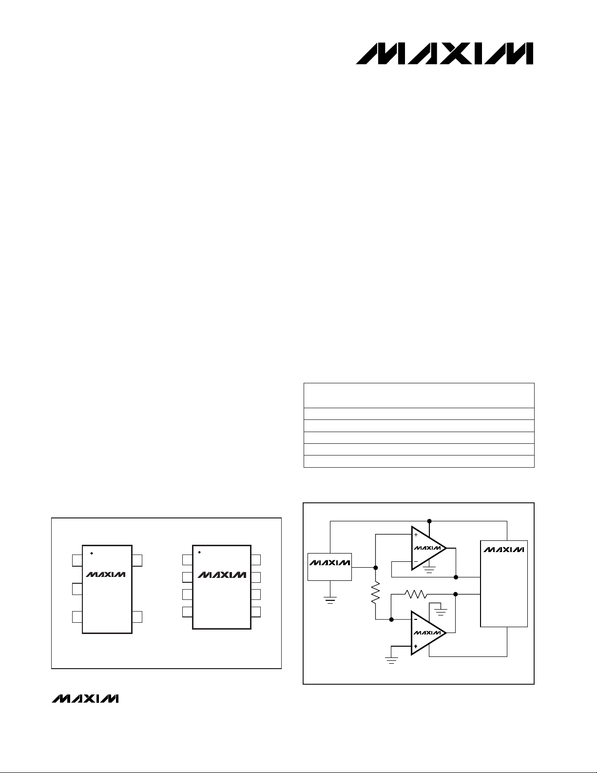
MAX4162 is available in 8-pin SO and space-saving
5-pin SOT23 packages. The MAX4163 is available in an
8-pin µMAX or SO, while the MAX4164 comes in a
14-pin SO.
________________________Applications
Battery-Powered Devices Medical Instruments
pH Probes Ionization Detectors
Portable Equipment Cellular Phones
Low-Power, Low-Voltage
Equipment
____________________________Features
♦ 5-Pin SOT23 Package (MAX4162)
♦ 1.0pA Typical Input Bias Current
♦ Fully Specified Single-Supply Operation
at 3V and 5V
♦ Input Common-Mode Voltage Range Extends
250mV Beyond Either Supply Rail
♦ Rail-to-Rail Output Swing
♦ 200kHz Gain-Bandwidth Product
♦ 25µA Quiescent Current per Amplifier
♦ Excellent CMRR, PSRR, and Gain Linearity
♦ No Phase Reversal for Overdriven Inputs
♦ Unity-Gain Stable
♦ Stable with Any Capacitive Load
♦ Internally Short-Circuit Protected to Either Rail
MAX4162/MAX4163/MAX4164
SOT23, Micropower, Single-Supply,
Rail-to-Rail I/O Op Amps
________________________________________________________________
Maxim Integrated Products
1
MAX152
MAX4162
MAX4162
MAX6120
MICROPOWER ±1.2V REFERENCE
V
REF+
V
DD
V
DD
V
DD
V
SS
V
SS
R
V
SS
-1.2V
+1.2V
V
OUT
V
OUT
GND
V
IN
3V
IN+
IN-
R
IN-
IN+
V
OUT
-3V
V
REF-
________Typical Application Circuit
_________________Pin Configurations
19-1195; Rev 0; 4/97
PART
MAX4162ESA
-40°C to +85°C
TEMP.
RANGE
PIN-
PACKAGE
8 SO
______________Ordering Information
For free samples & the latest literature: http://www.maxim-ic.com, or phone 1-800-998-8800
SOT
TOP MARK
—
TOP VIEW
V
SS
IN-
IN+
1
5
V
DD
OUT
MAX4162
SOT23-5
2
3
4
OUT
N.C.
V
SS
1
2
87N.C.
V
DD
IN-
IN+
N.C.
SO
3
4
6
5
MAX4162
MAX4162EUK -40°C to +85°C 5 SOT23-5 AABX
MAX4163ESA
-40°C to +85°C 8 SO —
MAX4163EUA -40°C to +85°C 8 µMAX —
MAX4164ESD
-40°C to +85°C 14 SO —
Pin Configurations continued at end of data sheet.
Rail-to-Rail is a registered trademark of Nippon-Motorola, Ltd.
MAX4162/MAX4163/MAX4164
SOT23, Micropower, Single-Supply,
Rail-to-Rail I/O Op Amps
2 _______________________________________________________________________________________
ABSOLUTE MAXIMUM RATINGS
ELECTRICAL CHARACTERISTICS: +3V Operation
(VDD=+3V, VSS= 0V, VCM= V
DD
/ 2, V
OUT
= V
DD
/ 2, RLtied to V
DD
/ 2, TA= -40°C to +85°C, unless otherwise noted. Typical values
are at T
A
= +25°C.)
Stresses beyond those listed under “Absolute Maximum Ratings” may cause permanent damage to the device. These are stress ratings only, and functional
operation of the device at these or any other conditions beyond those indicated in the operational sections of the specifications is not implied. Exposure to
absolute maximum rating conditions for extended periods may affect device reliability.
Supply Voltage (VDDto VSS)................................................+11V
IN+, IN-, OUT Voltage......................(V
DD
+ 0.3V) to (V
SS
- 0.3V)
Short-Circuit Duration (to either rail)...........................Continuous
Continuous Power Dissipation (T
A
= +70°C)
5-Pin SOT23 (derate 7.1mW/°C above +70°C)..............571mW
8-Pin SO (derate 5.88mW/°C above +70°C)..................471mW
8-Pin µMAX (derate 4.1mW/°C above +70°C)...............330mW
14-Pin SO (derate 8.00mW/°C above +70°C)................640mW
Operating Temperature Range ...........................-40°C to +85°C
Storage Temperature Range.............................-65°C to +150°C
Lead Temperature (soldering, 10sec).............................+300°C
To either supply rail
VOL- V
SS
VDD- V
OH
VOL- V
SS
VDD- V
OH
Inferred from PSRR test
RL= 10kΩ
Inferred from CMRR test
TA= +25°C
TA= -40°C to +85°C
TA= +25°C
TA= -40°C to +85°C
CONDITIONS
15Output Short-Circuit Current
mV
3 25
RL= 100kΩ
Output Voltage Swing
3 25
30 180
RL= 10kΩ
30 180
dBLarge-Signal Voltage Gain 85 120
dBCommon-Mode Rejection Ratio 70 100
pA1.0 100
V2.7 10.0Operating Voltage Range
Input Bias Current (Note 1)
TΩ
VSS- VDD+
0.25 0.25
Input Common-Mode Voltage Range
>10Differential Input Resistance
±6
±0.5 ±5
MAX4164
±0.5 ±3
Input Offset Voltage
±4
MAX4162
±0.5 ±4
mV
±5
MAX4163
UNITSMIN TYP MAXPARAMETER
AV= +1V/V
kHz200Gain-Bandwidth Product
VDD= 2.7V to 10VPower-Supply Rejection Ratio dB80 110
mA
0.1Closed-Loop Output Resistance
V
VCM= (VSS- 0.25V) to (VDD+ 0.25V)
Ω
µV/°CInput Offset Voltage Tempco 2
TA= +25°C
TA= -40°C to +85°C
µA25 40Supply Current (per amplifier)
degrees60Phase Margin
dB12Gain Margin
V
OUT
= 1V to 2V step µs50Settling Time to 0.1%
VDD= 0V to 3V step, VIN= VDD/ 2, AV= +1V/V µs20Turn-On Time
V/ms115Slew Rate
f = 1kHz, V
OUT
= 2Vp-p, RL= 100kΩ, AV= +1V/VTotal Harmonic Distortion %0.02
MAX4162/MAX4163/MAX4164
SOT23, Micropower, Single-Supply,
Rail-to-Rail I/O Op Amps
_______________________________________________________________________________________ 3
ELECTRICAL CHARACTERISTICS: +3V Operation (continued)
(VDD=+3V, VSS= 0V, VCM= V
DD
/ 2, V
OUT
= V
DD
/ 2, RLtied to V
DD
/ 2, TA= -40°C to +85°C, unless otherwise noted. Typical values
are at T
A
= +25°C.)
CONDITIONS UNITSMIN TYP MAXPARAMETER
pF1.5Input Common-Mode Capacitance
kHz700Internal Charge-Pump Frequency
µVp-p100Charge-Pump Output Feedthrough
f = 1kHz
nV/√Hz
80Input Noise Voltage Density
ELECTRICAL CHARACTERISTICS: +5V Operation
(VDD= +5V, VSS= 0V, VCM= V
DD
/ 2, V
OUT
= V
DD
/ 2, RLtied to V
DD
/ 2, TA= -40°C to +85°C, unless otherwise noted. Typical
values are at T
A
= +25°C.)
VOL- V
SS
VDD- V
OH
VOL- V
SS
VDD- V
OH
Inferred from PSRR test
Inferred from CMRR test
TA= +25°C
TA= -40°C to +85°C
TA= +25°C
TA= -40°C to +85°C
CONDITIONS
mV
5 40
RL= 100kΩ
Output Voltage Swing
5 40
50 300
RL= 10kΩ
50 300
dB85 120Large-Signal Voltage Gain
dBCommon-Mode Rejection Ratio 70 100
pA1.0 100
V2.7 10.0Operating Voltage Range
Input Bias Current (Note 1)
VSS- VDD+
0.25 0.25
Input Common-Mode Voltage Range
±6
MAX4164
±0.5 ±5
±0.5 ±3
Input Offset Voltage
±4
MAX4162
±0.5 ±4
mV
±5
MAX4163
UNITSMIN TYP MAXPARAMETER
VCM= (VSS- 0.25V) to (VDD+ 0.25V)
V
pF0.7Differential Input Capacitance
µA27 45Supply Current (per amplifier)
TΩ>10Differential Input Resistance
µV/°C2Input Offset Voltage Tempco
TA= +25°C
TA= -40°C to +85°C
AV= +1V/V
To either supply rail mAOutput Short-Circuit Current
0.1
15
Closed-Loop Output Resistance Ω
VDD= 4.5V to 10V dBPower-Supply Rejection Ratio
200
80 110
Gain-Bandwidth Product kHz
degreesPhase Margin
12
60
Gain Margin dB
MAX4162/MAX4163/MAX4164
SOT23, Micropower, Single-Supply,
Rail-to-Rail I/O Op Amps
4 _______________________________________________________________________________________
0
5
10
15
20
25
30
1 2 3 4 5 6 7
8
9
10
SUPPLY CURRENT
vs. SUPPLY VOLTAGE
MAX4162-01
SUPPLY VOLTAGE (V)
SUPPLY CURRENT (µA)
10
12
14
16
18
20
22
24
26
28
-40 -20 0 20
40
60 80 100
SUPPLY CURRENT
vs. TEMPERATURE
MAX4162-02
TEMPERATURE (°C)
SUPPLY CURRENT (µA)
VCC = 5V
VCC = 3V
-150
-130
-110
-90
-70
-50
-30
-10
10
30
50
1 2 3 4 5 6 7 8 9 10
INPUT OFFSET VOLTAGE VARIATION
vs. SUPPLY VOLTAGE
MAX4162-03
SUPPLY VOLTAGE (V)
V
OS
(µV)
ELECTRICAL CHARACTERISTICS: +5V Operation (continued)
(VDD= +5V, VSS= 0V, VCM= V
DD
/ 2, V
OUT
= V
DD
/ 2, RLtied to V
DD
/ 2, TA= -40°C to +85°C, unless otherwise noted. Typical
values are at T
A
= +25°C.)
f = 1kHz, V
OUT
= 2Vp-p, RL= 100kΩ, AV= +1V/V %0.02Total Harmonic Distortion
V/ms115Slew Rate
V
OUT
= 1V to 4V step µs70Settling Time to 0.1%
VDD= 0V to 5V step, VIN= V
DD
/ 2, AV= +1V/V µs40
CONDITIONS
Turn-On Time
f = 1kHz
nV/√Hz
80Input Noise Voltage Density
pF1.5Input Common-Mode Capacitance
MHz700Internal Charge-Pump Frequency
µVp-p100Charge-Pump Output Feedthrough
UNITSMIN TYP MAXPARAMETER
__________________________________________Typical Operating Characteristics
(VDD= +5V, VSS= 0V, VCM= V
DD
/ 2, TA = +25°C, unless otherwise noted.)
Note 1: Input bias current guaranteed by design, not production tested.
Note 2: The MAX4162EUK specifications are 100% tested at T
A
= +25°C. Limits over the extended temperature range are
guaranteed by design, not production tested.
pF0.7Differential Input Capacitance

MAX4162/MAX4163/MAX4164
SOT23, Micropower, Single-Supply,
Rail-to-Rail I/O Op Amps
_______________________________________________________________________________________
5
-1000
-750
-500
-250
0
250
500
750
1000
-40 -20 0
20
40 60 80 100
INPUT OFFSET VOLTAGE
vs. TEMPERATURE
MAX4162-04
TEMPERATURE (°C)
V
OS
(µV)
-14
-12
-10
-8
-6
-4
-2
0
2
4
6
-0.5 0.5 1.5 2.5 3.5 4.5 5.5
INPUT OFFSET VOLTAGE VARIATION
vs. COMMON-MODE VOLTAGE
MAX4162-05
COMMON-MODE VOLTAGE (V)
V
OS
(µV)
10
30
50
70
90
110
130
0.1 1 10 100 1k 10k 100k 1M
POWER-SUPPLY REJECTION RATIO
vs. FREQUENCY
MAX4162-08
FREQUENCY (Hz)
PSRR (dB)
AV = +1
0
10
20
30
40
50
70
60
80
100
90
110
120
COMMON-MODE REJECTION
vs. TEMPERATURE
MAX4162-10
TEMPERATURE (°C)
COMMON-MODE REJECTION (dB)
-40 -20 0 20
40
60 80 100
VDD = 3V OR 5V
V
CM
= -0.25V TO VDD + 0.25V
10
30
50
70
90
110
130
-40 -20 0 20
40
60 80 100
POWER-SUPPLY REJECTION RATIO
vs. TEMPERATURE
MAX4162-09
TEMPERATURE (°C)
PSRR (dB)
0
20
40
60
80
100
120
140
160
OPEN-LOOP GAIN
vs. TEMPERATURE
MAX4162-11
TEMPERATURE (°C)
OPEN-LOOP GAIN (dB)
-40 -20 0 20
40
60 80 100
VDD = 3V OR 5V
RL = 10kΩ
RL = 100kΩ
0.1
1
10
100
1000
10,000
0.1 1
10
100 1k 10k 100k 1M
OUTPUT IMPEDANCE
vs. FREQUENCY
MAX4162-12a
FREQUENCY (Hz)
OUTPUT IMPEDANCE (Ω)
AV = +1
____________________________Typical Operating Characteristics (continued)
(VDD= +5V, VSS= 0V, VCM= V
DD
/ 2, TA = +25°C, unless otherwise noted.)
0
5
10
15
20
25
30
35
40
SHORT-CIRCUIT OUTPUT CURRENT
vs. TEMPERATURE
MAX4162-13
TEMPERATURE (°C)
SHORT-CIRCUIT OUTPUT CURRENT (mA)
-40 -20 0 20
40
60 80 100
VDD = 3V OR 5V
SHORT TO EITHER SUPPLY RAIL
1.00
1.25
1.50
1.75
2.00
0 2.50 3.751.25
5.00
COMMON-MODE INPUT CAPACITANCE
vs. COMMON-MODE VOLTAGE
MAX4162-12b
COMMON-MODE VOLTAGE (V)
COMMON-MODE INPUT CAPACITANCE (pF)

MAX4162/MAX4163/MAX4164
SOT23, Micropower, Single-Supply,
Rail-to-Rail I/O Op Amps
6 _______________________________________________________________________________________
0
50
100
150
200
250
300
0 0.4 0.8 1.2 1.6 2.0
MAXIMUM OUTPUT VOLTAGE
vs. LOAD CURRENT
MAX4162-14
LOAD CURRENT (mA)
V
DD
- V
OUT(MAX)
(mV)
VDD = 3V OR 5V
LOAD TO V
DD
/ 2
0
50
100
150
200
250
300
0 0.4 0.8 1.2 1.6 2.0
MINIMUM OUTPUT VOLTAGE
vs. LOAD CURRENT
MAX4162-15
LOAD CURRENT (mA)
V
OUT(MIN)
(mV)
VDD = 3V OR 5V
LOAD TO V
DD
/ 2
0
10
20
30
40
50
60
70
80
90
100
MAXIMUM OUTPUT VOLTAGE
vs. TEMPERATURE
(V
DD
= 5V)
MAX4162-16
TEMPERATURE (°C)
V
DD
- V
OUT(MAX)
(mV)
-40 -20 0 20
40
60 80 100
VDD = 5V
LOAD TO V
DD
/ 2
RL = 5kΩ
RL = 10kΩ
RL = 100kΩ
0
10
20
30
40
50
60
70
80
90
MINIMUM OUTPUT VOLTAGE
vs. TEMPERATURE
(V
DD
= 3V)
MAX4162-19
TEMPERATURE (°C)
V
OUT(MIN)
(mV)
-40 -20 0 20
40
60 80 100
VDD = 3V
LOAD TO V
DD
/ 2
RL = 5kΩ
RL = 10kΩ
RL = 100kΩ
0
20
40
60
80
100
120
140
MINIMUM OUTPUT VOLTAGE
vs. TEMPERATURE
(V
DD
= 5V)
MAX4162-17
TEMPERATURE (°C)
V
OUT(MIN)
(mV)
-40 -20 0 20
40
60 80 100
VDD = 5V
LOAD TO V
DD
/ 2
RL = 5kΩ
RL = 10kΩ
RL = 100kΩ
0
10
20
30
40
50
60
MAXIMUM OUTPUT VOLTAGE
vs. TEMPERATURE
(V
DD
= 3V)
MAX4162-18
TEMPERATURE (°C)
V
DD
- V
OUT(MAX)
(mV)
-40 -20 0 20
40
60 80 100
VDD = 3V
LOAD TO V
DD
/ 2
RL = 5kΩ
RL = 10kΩ
RL = 100kΩ
0
20
40
60
80
100
120
-0.5 0.5 1.5 2.5 3.5 4.5 5.5
NOISE VOLTAGE DENSITY
vs. COMMON-MODE VOLTAGE
MAX4162-20
NOISE VOLTAGE DENSITY (nV/√Hz)
100Hz
1kHz
10kHz
0
10
20
30
40
50
60
70
80
90
100
10 100 1k 10k 1M100k
NOISE VOLTAGE DENSITY
vs. FREQUENCY
MAX4162-21a
FREQUENCY (Hz)
NOISE VOLTAGE DENSITY (nV/√Hz )
0.001
0.01
0.1
1
10 1k100
10k
TOTAL HARMONIC DISTORTION
PLUS NOISE vs. FREQUENCY
MAX4162-21b
FREQUENCY (Hz)
THD + NOISE (%)
AV = +1
R
L
= 100kΩ
Vp-p = 4.99V
Vp-p = 1V
____________________________Typical Operating Characteristics (continued)
(VDD= +5V, VSS= 0V, VCM= V
DD
/ 2, TA = +25°C, unless otherwise noted.)

MAX4162/MAX4163/MAX4164
SOT23, Micropower, Single-Supply,
Rail-to-Rail I/O Op Amps
_______________________________________________________________________________________
7
60
-40
1 100 1k 10k 100k 1M
GAIN AND PHASE vs. FREQUENCY
(C
L
= 0pF)
-20
MAX4162-22
FREQUENCY (Hz)
GAIN (dB)
PHASE (degrees)
0
20
40
180
-180
-108
-36
36
108
144
-144
-72
0
72
RL = 100kΩ
C
L
= 0pF
A
V
= +1000
GAIN
PHASE
60
-40
1 100 1k 10k 100k 1M
GAIN AND PHASE vs. FREQUENCY
(C
L
= 500pF)
-20
MAX4162-23
FREQUENCY (Hz)
GAIN (dB)
PHASE (degrees)
0
20
40
180
-180
-108
-36
36
108
144
-144
-72
0
72
RL = 100kΩ
C
L
= 500pF
A
V
= +1000
GAIN
PHASE
60
-40
1 100 1k 10k 100k 1M
GAIN AND PHASE vs. FREQUENCY
(C
L
= 0.01µF)
-20
MAX4162-24
FREQUENCY (Hz)
GAIN (dB)
PHASE (degrees)
0
20
40
180
-180
-108
-36
36
108
144
-144
-72
0
72
RL = 100kΩ
C
L
= 0.01µF
A
V
= +1000
GAIN
PHASE
0.01
0.1
1
1.0 1.5 2.0 2.5 3.0 3.5 4.0 4.5
5.0
TOTAL HARMONIC DISTORTION PLUS NOISE
vs. OUTPUT VOLTAGE SWING
MAX4162-21c
PEAK-TO-PEAK OUTPUT VOLTAGE SWING (V)
THD + NOISE (%)
f = 5kHz
AV = +1
R
L
= 100kΩ
f = 1kHz
____________________________Typical Operating Characteristics (continued)
(VDD= +5V, VSS= 0V, VCM= V
DD
/ 2, TA = +25°C, unless otherwise noted.)
IN
(50mV/
div)
OUT
(50mV/
div)
NONINVERTING
SMALL-SIGNAL PULSE RESPONSE
(V
DD
= 3V, CL = 0pF)
MAX4162-25
TIME (100µs/div)
VDD = 3V, VIN = 100mV, RL = 100kΩ to V
DD
/ 2,
C
L
= 0pF
IN
(50mV/
div)
OUT
(50mV/
div)
NONINVERTING
SMALL-SIGNAL PULSE RESPONSE
(V
DD
= 3V, CL = 1500pF)
MAX4162-26
TIME (100µs/div)
VDD = 3V, VIN = 100mV, RL = 100kΩ to V
DD
/ 2,
C
L
= 1500pF

MAX4162/MAX4163/MAX4164
SOT23, Micropower, Single-Supply,
Rail-to-Rail I/O Op Amps
8 _______________________________________________________________________________________
IN
(2V/
div)
OUT
(2V/
div)
NONINVERTING
LARGE-SIGNAL PULSE RESPONSE
(V
DD
= 5V, CL = 0pF)
MAX4162-31
TIME (100µs/div)
VDD = 5V, VIN = 4V, RL = 100kΩ to V
DD
/ 2,
C
L
= 0pF
____________________________Typical Operating Characteristics (continued)
(VDD= +5V, VSS= 0V, VCM= V
DD
/ 2, TA = +25°C, unless otherwise noted.)
IN
(50mV/
div)
OUT
(50mV/
div)
NONINVERTING
SMALL-SIGNAL PULSE RESPONSE
(V
DD
= 5V, CL = 1500pF)
MAX4162-28
TIME (100µs)
VDD = 5V, VIN = 100mV, RL = 100kΩ to V
DD
/ 2,
C
L
= 1500pF
IN
(1V/
div)
OUT
(1V/
div)
NONINVERTING
LARGE-SIGNAL PULSE RESPONSE
(V
DD
= 3V, CL = 0pF)
MAX4162-29
TIME (100µs/div)
VDD = 3V, VIN = 2V, RL = 100kΩ to V
DD
/ 2,
C
L
= 0pF
IN
(1V/
div)
OUT
(1V/
div)
NONINVERTING
LARGE-SIGNAL PULSE RESPONSE
(V
DD
= 3V, CL = 1500pF)
MAX4162-30
TIME (100µs/div)
VDD = 3V, VIN = 2V, RL = 100kΩ to V
DD
/ 2,
C
L
= 1500pF
IN
(50mV/
div)
OUT
(50mV/
div)
NONINVERTING
SMALL-SIGNAL PULSE RESPONSE
(V
DD
= 5V, CL = 0pF)
MAX4162-27
TIME (100µs/div)
VDD = 5V, VIN = 100mV, RL = 100kΩ to V
DD
/ 2,
C
L
= 0pF

MAX4162/MAX4163/MAX4164
SOT23, Micropower, Single-Supply,
Rail-to-Rail I/O Op Amps
_______________________________________________________________________________________ 9
______________________________________________________________Pin Description
SO
1, 5, 8
3
4
—
7
6
SOT23-5
—
3
2
—
5
1
____________________________Typical Operating Characteristics (continued)
(VDD= +5V, VSS= 0V, VCM= V
DD
/ 2, TA = +25°C, unless otherwise noted.)
MAX4162
MAX4163
SO/µMAX
—
—
—
4
8
1
MAX4164
SO
—
11
—
4
1
No Connection. Not internally connected.
— Amplifier Noninverting Input
Negative Power Supply
Amplifier Output
Positive Power Supply
Amplifier A Output
N.C.
IN+
V
SS
OUT
V
DD
OUTA
INA-— Amplifier A Inverting Input— 2 2
IN-2 Amplifier Inverting Input4 — —
INA+— Amplifier A Noninverting Input— 3 3
INB+— Amplifier B Noninverting Input— 5 5
INB-— Amplifier B Inverting Input— 6 6
OUTB— Amplifier B Output— 7 7
OUTC— Amplifier C Output— — 8
INC-— Amplifier C Inverting Input— — 9
INC+— Amplifier C Noninverting Input— — 10
IND+— Amplifier D Noninverting Input— — 12
IND-— Amplifier D Inverting Input— — 13
OUTD— Amplifier D Output— — 14
NAME FUNCTION
PIN
LARGE-SIGNAL PULSE RESPONSE
(V
DD
IN
(2V/
div)
OUT
(2V/
div)
VDD = 5V, VIN = 4V, RL = 100kΩ to V
= 1500pF
C
L
NONINVERTING
= 5V, CL = 1500pF)
TIME (100µs/div)
DD
MAX4162-32
/ 2,
MAX4163/MAX4164
CROSSTALK vs. FREQUENCY
0
-20
-40
-60
-80
-100
CROSSTALK (dB)
-120
-140
-160
0.1 1 10 100 1000
FREQUENCY (kHz)
MAX4162-40

__________Applications Information
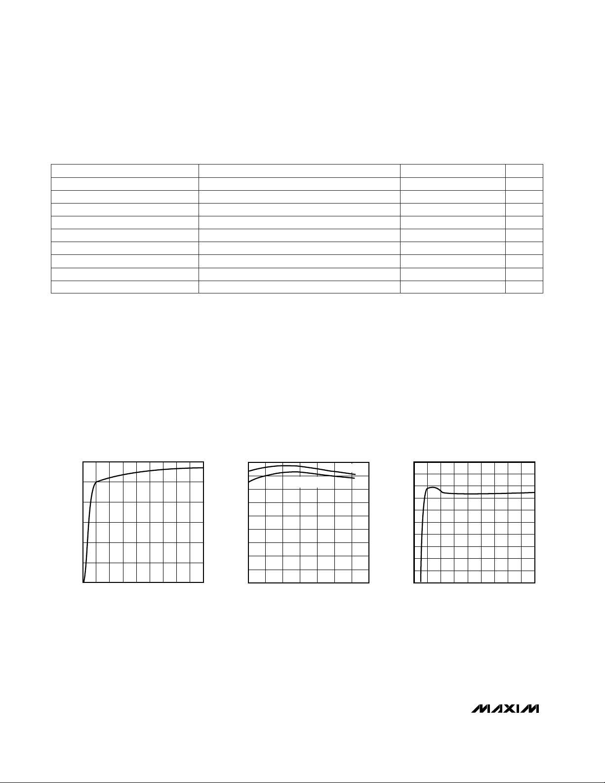
Rail-to-Rail Inputs and Outputs
The MAX4162/MAX4163/MAX4164 input common-mode
range extends 250mV
beyond
each of the supply rails,
providing a substantial increase in dynamic range over
other op amps (even many of those referred to as rail-torail). Although the minimum operating voltage is specified at 2.7V, the devices typically provide full rail-to-rail
operation below 2.0V (Figure 1). These amplifiers do not
suffer from midswing common-mode-rejection degrada-
tion or crossover nonlinearity often encountered in other
rail-to-rail op amps. Extremely low, 1.0pA input bias current makes these devices ideal for applications such as
pH probes, electrometers, and ionization detectors.
They are also protected against phase reversal (inferred
from CMRR test) and latchup for input signals extending
beyond the supply rails. The output stage achieves a
lower output impedance than traditional rail-to-rail output stages, providing an output voltage range that typically swings within 150mV of the supply rails for 1mA
loads. This architecture also maintains high open-loop
gain and output swing while driving substantial loads.
Output Loading and Stability
These devices drive 1mA loads to within 150mV of the
supply rails while consuming only 25µA of quiescent
current. Internal compensation allows these amplifiers to
remain unity-gain stable while driving any capacitive
load (Figure 2).
Internal Charge Pump
An internal charge pump provides two internal supplies
typically 2V beyond each rail. These internal rails allow
the MAX4162/MAX4163/MAX4164 to achieve true railto-rail inputs and outputs, while providing excellent
common-mode rejection, power-supply rejection ratios,
and gain linearity.
These charge pumps require no external components,
and in most applications are entirely transparent to the
user. Two characteristics may be visible to the user,
depending on the application:
MAX4162/MAX4163/MAX4164
SOT23, Micropower, Single-Supply,
Rail-to-Rail I/O Op Amps
10 ______________________________________________________________________________________
IN
(200mV/
div)
500mV
0mV
500mV
0mV
OUT
(200mV/
div)
LARGE CAPACITIVE-LOAD DRIVE
MAX4162-36
TIME (5µs/div)
AV = +1, CL = 1µF, RL = 100kΩ
Figure 2. Large Capacitive-Load Drive
IN
(0.667V/
div)
2V
0V
2V
0V
OUT
(0.667V/
div)
RAIL-TO-RAIL
INPUT/OUTPUT VOLTAGE RANGE
(V
DD
= 2V)
MAX4162-34
TIME (200µs/div)
VDD = 2V, V
PP
= 2V, f = 1kHz, RL = 10kΩ
Figure 1. Rail-to-Rail I/O: a) VDD= 3V; b) VDD= 2V
IN
(1V/
div)
3V
0V
3V
0V
OUT
(1V/
div)
RAIL-TO-RAIL
INPUT/OUTPUT VOLTAGE RANGE
(V
DD
= 3V)
MAX4162-35
TIME (200µs/div)
VDD = 3V, VPP = 3V, f = 1kHz, RL = 10kΩ
a)
b)

MAX4162/MAX4163/MAX4164
SOT23, Micropower, Single-Supply,
Rail-to-Rail I/O Op Amps
______________________________________________________________________________________ 11
1) The on-board charge pumps generate a small
amount of 700kHz switching noise at the op amp’s
output. The amplitude of this noise is typically
100µVp-p. The noise is not referred to the input, and
is independent of amplifier gain. The charge-pump
switching frequency is well beyond the amplifier’s
200kHz bandwidth, and is therefore unnoticeable in
most applications.
2) The charge pumps typically require up to 20µs on
power-up to fully energize the internal supply rails
(Figure 3).
Power Supplies and Layout
The MAX4162/MAX4163/MAX4164 are guaranteed to
operate from a single +2.7V to +10.0V power supply, but
full rail-to-rail operation typically extends below 2V. For
single-supply operation, bypass the power supply with a
1µF capacitor in parallel with a 0.1µF ceramic capacitor.
If operating from dual supplies, bypass each supply to
ground.
Good layout improves performance by decreasing the
amount of stray capacitance at the op amp’s inputs and
output. To decrease stray capacitance, minimize both
trace and external component lead lengths, and place
external components close to the op amp’s pins.
IN
(1.5V/
div)
3V
0V
1.5V
0V
OUT
(750mV/
div)
POWER-UP TRANSIENT
(V
DD
= 3V)
MAX4162-38
TIME (100µs/div)
VDD = 3V, VIN = V
DD
/ 2, RL = 10kΩ, CL = 1500pF
Figure 3. Power-Up Transient: a) VDD= 3V; b) VDD= 5V
a)
b)
_____________________________________________Pin Configurations (continued)
TOP VIEW
INB-
INB+
V
SS
1
2
8
7
V
DD
OUTB
INAINA+
OUTA
SO/µMAX
3
4
6
5
MAX4163
14
13
12
11
10
9
8
1
2
3
4
5
6
7
OUTD
INDIND+
V
SS
V
DD
INA+
INA-
OUTA
MAX4164
INC+
INCOUTC
OUTB
INB-
INB+
SO
(2V/
div)
OUT
(1V/
div)
IN
POWER-UP TRANSIENT
= 5V)
(V
DD
MAX4162-39
5V
0V
2.5V
0V
VDD = 5V, VIN = V
TIME (100µs/div)
/ 2, RL = 10kΩ, CL = 1500pF
DD

Maxim cannot assume responsibility for use of any circuitry other than circuitry entirely embodied in a Maxim product. No circuit patent licenses are
implied. Maxim reserves the right to change the circuitry and specifications without notice at any time.
12
__________________Maxim Integrated Products, 120 San Gabriel Drive, Sunnyvale, CA 94086 (408) 737-7600
© 1997 Maxim Integrated Products Printed USA is a registered trademark of Maxim Integrated Products.
MAX4162/MAX4163/MAX4164
SOT23, Micropower, Single-Supply,
Rail-to-Rail I/O Op Amps
4.0 ±0.1
0.30 ±0.05
0.8 ±0.05
0.30R MAX.
Bo
Ko
2.2 ±0.1
0.5 RADIUS
TYPICAL
A0
4.0 ±0.1
2.0 ±0.05
1.5 +0.1/-0.0 DIAMETER
1.75 ±0.1
1.0 ±0.1
A
8.0 ±0.3
3.5 ±0.05
1.0 MINIMUM
A
Ao = 3.1mm ±0.1
Bo = 2.7mm ±0.1
Ko = 1.2mm ±0.1
NOTE: DIMENSIONS ARE IN MM.
AND FOLLOW EIA481-1 STANDARD.
__________________________________________________Tape-and-Reel Information
________________________________________________________Package Information
___________________Chip Information
MAX4162 TRANSISTOR COUNT: 291
MAX4163 TRANSISTOR COUNT: 496
MAX4164 TRANSISTOR COUNT: 992
SOT5L.EPS
 Loading...