

_______________General Description
The MAX4147 differential line driver offers high-speed
performance while consuming only 100mW of power.
Its amplifier has fully symmetrical inputs and outputs
and uses laser-trimmed, matched, thin-film resistors to
deliver 70dB CMR at 10MHz. Using current-feedback
techniques, the MAX4147 achieves a 300MHz bandwidth and a 2000V/µs slew rate.
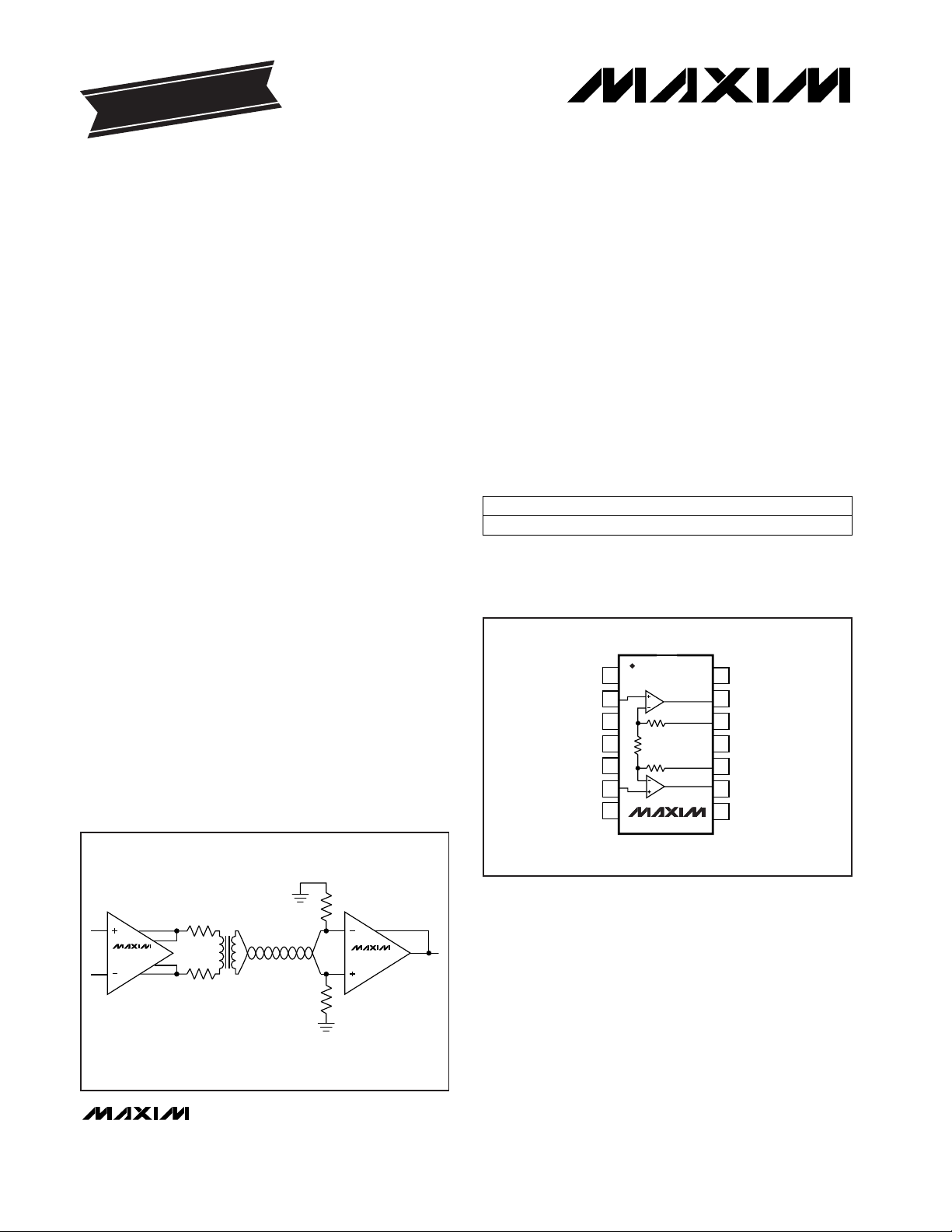
Optimized for differential, high-output-current applications such as transformer drivers, the MAX4147 drives
±2.6V into a 26.5Ω load (single-ended) or ±5.6V into a
53Ω load (differential). This device is preset for a
closed-loop gain of 2V/V. Its ultra-low 0.008%/0.03° differential gain/phase allow for a variety of video and RF
signal-processing applications.
For power-sensitive applications, the MAX4147 has a
shutdown function that reduces supply current to less
than 1mA. In addition, superior SFDR (-82dBc at
10kHz, RL= 33Ω) makes it ideal as a transformer driver
for HDSL applications.
For a complete differential transmission link, use the
MAX4147 with the MAX4144 line receiver (see the
MAX4144 data sheet for more information).
________________________Applications
VDSL, ADSL, HDSL
Video Twisted-Pair Driver
Differential Pulse Amplifier
Differential ADC Driver
____________________________Features
♦ 2V/V Fixed Gain
♦ 300MHz -3dB Bandwidth
♦ 2000V/µs Slew Rate
♦ 82dBc SFDR at 10kHz
♦ 70dB CMR at 10MHz
♦ Low Differential Gain/Phase: 0.008%/0.03°
♦ High Output Drive: ±5.6V into 53Ω
♦ Low Power: 100mW
MAX4147
300MHz, Low-Power,
High-Output-Current, Differential Line Driver
________________________________________________________________
Maxim Integrated Products
1
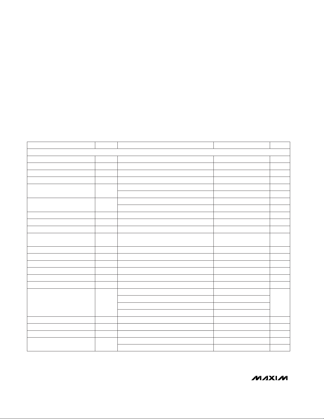
14
13
12
11
10
9
8
1
2
3
4
5
6
7
V
CC
OUT+
SENSE+
GND
SHDN
N.C.
IN+
V
EE
TOP VIEW
MAX4147
SENSEOUTV
CC
V
EE
IN-
N.C.
SO
R
f
R
f
R
G
__________________Pin Configuration
MAX4144
MAX4147
OUT
OUT+
OUT-
IN-
IN+
IN-
IN+
SENSE
SENSE+
SENSE-
R
t
R
t
R
t
R
t
VDSL
TRANSFORMER ISOLATION
________Typical Application Circuit
19-1106; Rev 1; 11/96
PART
MAX4147ESD -40°C to +85°C
TEMP. RANGE PIN-PACKAGE
14 SO
EVALUATION KIT
AVAILABLE
______________Ordering Information
For free samples & the latest literature: http://www.maxim-ic.com, or phone 1-800-998-8800.
For small orders, phone 408-737-7600 ext. 3468.
MAX4147
300MHz, Low-Power,
High-Output-Current, Differential Line Driver
2 _______________________________________________________________________________________
ABSOLUTE MAXIMUM RATINGS
ELECTRICAL CHARACTERISTICS
(VCC= +5V, VEE= -5V, TA= T
MIN
to T
MAX
, unless otherwise noted. Typical values are at TA= +25°C.)
Stresses beyond those listed under “Absolute Maximum Ratings” may cause permanent damage to the device. These are stress ratings only, and functional
operation of the device at these or any other conditions beyond those indicated in the operational sections of the specifications is not implied. Exposure to
absolute maximum rating conditions for extended periods may affect device reliability.
Supply Voltage (VCCto VEE)..................................................12V
Voltage on Any Input to Ground ......(V
CC
+ 0.3V) to (VEE- 0.3V)
Continuous Power Dissipation (T
A
= +70°C)
SO (derate 8.33mW/°C above +70°C).........................667mW
Short-Circuit Duration.........................................................10sec
Operating Temperature Range
MAX4147ESD ..................................................-40°C to +85°C
Storage Temperature Range.............................-65°C to +160°C
Lead Temperature (soldering, 10sec).............................+300°C
V
OUT
= ±2.2V
V
OUT
= 0V, RL= ∞
Differential, RL= ∞
Single-ended, RL= ∞
V
OUT
= 0V, RL= ∞
VIN= 0, RL= ∞
VIN= 0, RL= ∞
VS= ±4.5V to ±5.5V
VCM= ±2.8V
f = 10kHz
V
OUT
= 0V, RL= ∞, VIN= -V
OS
V
OUT
= 0V, RL= ∞, VIN= -V
OS
RL= ∞
CONDITIONS
V0.8V
IL
SHDN Low Threshold
V2.0V
IH
SHDN High Threshold
mA110 160I
OUT
Output Current Drive
7.2 7.8
3.2 3.8
mA0.6 1I
SHDN
Shutdown Supply Current
mA10 13I
SY
Quiescent Supply Current
dB70 100PSRPower-Supply Rejection
dB70 100CMRCommon-Mode Rejection
V/V
0.3 1
A
V
Gain 2
V-2.8 2.8V
CM
Common-Mode Input Voltage
Range
-3.6 3.6
µV/°C30TCV
OS
Input Offset Voltage Drift
mV0.5 6V
OS
Input Offset Voltage
MΩ1Differential Input Resistance
pF1C
IN
Input Capacitance
1.7
µA9 20I
B
Input Bias Current
µA0.03 2I
OS
Input Offset Current
8
nV/√Hz
80
e
n
Input Voltage Noise
UNITSMIN TYP MAXSYMBOLPARAMETER
f = 10kHz
f = 1MHz to 100MHz
RL= ∞
-1V ≤ V
OUT
≤ +1V, RL= 53Ω
-1V ≤ V
OUT
≤ +1V, RL= 53Ω
V
SHDN
≤ 0.8V µA75 150
I
SHDN
SHDN Input Current
f = 1MHz to 100MHz
pA/√Hz
17
I
n
Input Current Noise
Differential Input Voltage Range
V
Gain Error %
Differential, RL= 53Ω
Single-ended, RL= 26.5Ω
V
5.0 5.6
|
V
OUT
|
Output Voltage Swing
2.2 2.6
µV
RMS
nA
RMS
DC SPECIFICATIONS
V
SHDN
≥ 2V 10 nA
MAX4147
300MHz, Low-Power,
High-Output-Current, Differential Line Driver
_______________________________________________________________________________________ 3
ELECTRICAL CHARACTERISTICS (continued)
(VCC= +5V, VEE= -5V, TA= T
MIN
to T
MAX
, unless otherwise noted. Typical values are at TA= +25°C.)
CONDITIONS UNITSMIN TYP MAXSYMBOLPARAMETER
300
V
OUT
= 2Vp-p
V
OUT
≤ 0.1V
RMS
MHz
250
BW
(-3dB)
-3dB Bandwidth
f = 10MHz 70
70V
OUT
≤ 0.1V
RMS
MHzBW
(0.1dB)
0.1dB Bandwidth
f = 3.58MHz, RL= 150Ω 0.008
Differential, -2V ≤ V
OUT
≤ +2V 2000
fC= 5MHz, V
OUT
= 2Vp-p,
RL= 150Ω differential, Figure 2
dBc
-75
SFDRSpurious-Free Dynamic Range
fC= 10kHz, V
OUT
= 4.0Vp-p, RL= 33Ω single-
ended, RS= 50Ω, Figure 1
-82
f = 3.58MHz, RL= 150Ω 0.03
ns
10
t
s
Settling Time
1V ≤ V
OUT
≤ +1V, RL= 150Ω,
A
VCL
= +2
30
MHz
dB
V/µs
%
degrees
SRSlew Rate
DPDifferential Phase
DGDifferential Gain
CMRCommon-Mode Rejection
FPBWFull-Power Bandwidth
to 0.1%
to 0.01%
AC SPECIFICATIONS

MAX4147
300MHz, Low-Power,
High-Output-Current, Differential Line Driver
4 _______________________________________________________________________________________
__________________________________________Typical Operating Characteristics
(VCC= +5V, VEE= -5V, RL = 150Ω, TA = +25°C, unless otherwise noted.)
11
1
100k 1M
10M 100M 1G
SMALL-SIGNAL GAIN
vs. FREQUENCY
3
MAX4147 TOC-01
FREQUENCY (Hz)
GAIN (dB)
5
7
9
10
2
4
6
8
A
VCL
= +2
11
1
100k 1M 100M10M 1G
LARGE-SIGNAL GAIN
vs. FREQUENCY
3
MAX4147-02
FREQUENCY (Hz)
GAIN (dB)
5
7
9
2
4
6
8
10
110
10
100k 1M 10M 100M
COMMON-MODE REJECTION
vs. FREQUENCY
30
MAX4147 TOC-02
FREQUENCY (Hz)
CMR (dB)
50
70
90
100
20
40
60
80
110
10
100k 1M 100M10M
POWER-SUPPLY REJECTION
vs. FREQUENCY
30
MAX4147-04
FREQUENCY (Hz)
PSR (dB)
50
70
90
20
40
60
80
100
10,000
0.1
100k 1M 100M10M
CLOSED-LOOP OUTPUT IMPEDANCE
vs. FREQUENCY
1
MAX4147-06
FREQUENCY (Hz)
OUTPUT IMPEDANCE (Ω)
10
100
1000
0.32
3.16
31.6
316.2
3162.3
TIME (10ns/div)
SMALL-SIGNAL
PULSE RESPONSE
IN
OUT
GND
GND
VOLTAGE (20mV/div)
A
VCL
= +2
TIME (10ns/div)
LARGE-SIGNAL
PULSE RESPONSE
IN
OUT
GND
GND
VOLTAGE (500mV/div)
A
VCL
= +2
0
5
10
15
20
25
30
35
0 50 100 150 250200
ISOLATION RESISTANCE
vs. CAPACITATIVE LOAD
MAX4144/4147-07
CAPACITATIVE LOAD (pF)
ISOLATION RESISTANCE (Ω)

MAX4147
300MHz, Low-Power,
High-Output-Current, Differential Line Driver
_______________________________________________________________________________________
5
100
10
1
10 1M100k10k1k100
VOLTAGE NOISE
vs. FREQUENCY
MAX4147-08
FREQUENCY (Hz)
VOLTAGE NOISE (nV/√Hz)
100
10
1
10 1M100k10k1k100
CURRENT NOISE
vs. FREQUENCY
MAX4147-09
FREQUENCY (Hz)
CURRENT NOISE (nA/√Hz)
0
-100
0 200 600 1000
5MHz HARMONIC DISTORTION
vs. LOAD
-80
-20
MAX4144/4147-10
LOAD (Ω)
HARMONIC DISTORTION (dBc)
400 800
-40
-60
-90
-70
-10
-30
-50
2ND HARMONIC
3RD HARMONIC
-50
-40
-30
-100
100k 1M
10M 100M
HARMONIC DISTORTION
vs. FREQUENCY
-90
MAX4147 TOC-05
FREQUENCY (Hz)
HARMONIC DISTORTION (dBc)
-80
-70
-60
A
VCL
= +2V
V
0
= 2Vp-p
2ND HARMONIC
3RD HARMONIC
12
11
10
9
8
7
-75 -25 25 75 125-50 0 50 100
POWER-SUPPLY CURRENT
vs. TEMPERATURE
MAX4144/4147-14
TEMPERATURE (°C)
CURRENT (mA)
0
-100
0 1 2 3 4
5MHz HARMONIC DISTORTION
vs. OUTPUT SWING
-80
-20
MAX4144/4147-12
OUTPUT SWING (Vp-p)
HARMONIC DISTORTION (dBc)
-40
-60
-90
-70
-10
-30
-50
2ND HARMONIC
3RD HARMONIC
4
6
8
10
12
14
16
18
0 50 100 150 250200
OUTPUT SWING
vs. LOAD RESISTANCE
MAX4144/4147-13
LOAD (Ω)
OUTPUT SWING (Vp-p)
2.0
1.5
1.0
0.5
0
-1.0
-0.5
-75 -25 25 75 125-50 0 50 100
INPUT OFFSET VOLTAGE
vs. TEMPERATURE
MAX4144/4147-15
TEMPERATURE (°C)
VOLTAGE (mV)
16
14
12
10
8
4
6
-75 -25 25 75 125-50 0 50 100
INPUT BIAS CURRENT
vs. TEMPERATURE
MAX4144/4147-16
TEMPERATURE (°C)
CURRENT (µA)
____________________________Typical Operating Characteristics (continued)
(VCC= +5V, VEE= -5V, RL = 150Ω, TA = +25°C, unless otherwise noted.)

MAX4147
300MHz, Low-Power,
High-Output-Current, Differential Line Driver
6 _______________________________________________________________________________________
____________________________Typical Operating Characteristics (continued)
(VCC= +5V, VEE= -5V, RL = 150Ω, TA = +25°C, unless otherwise noted.)
8.2
8.1
8.0
7.9
7.8
7.6
7.7
-75 -25 25 75 125-50 0 50 100
DIFFERENTIAL OUTPUT VOLTAGE SWING
vs. TEMPERATURE
MAX4144/4147-17
TEMPERATURE (°C)
VOLTAGE (V)
+16
-4
100k 1M 100M10M
SMALL-SIGNAL GAIN
vs. FREQUENCY AND CAPACITIVE LOAD
0
MAX4147-18
FREQUENCY (Hz)
GAIN (dB)
+4
+8
+12
-2
+2
+6
+10
+14
CL = 15pF
CL = 10pF
CL=5pF
-0.005
0.005
0.006
0.000
-0.010
-0.020
-0.01
0 100
0 100
DIFFERENTIAL GAIN
AND PHASE
0.01
0.00
IRE
IRE
PHASE (deg) GAIN (%)
0.03
0.04
0.02
MAX4147 TOC-06
AV = +2V/V
AV = +2V/V
______________________________________________________________Pin Description
NAME FUNCTION
1, 7 V
EE
Negative Power Supply. Connect to -5V.
2 IN+ Noninverting Input
PIN
3, 5 N.C. No Connect. Not internally connected.
8, 14 V
CC
Positive Power Supply
6 IN- Inverting Input
4 SHDN
Logic Input for Shutdown Circuitry. A logic low enables the amplifier. A logic high disables the
amplifier. The amplifier outputs are high impedance in shutdown mode; thus the impedances seen at
OUT+ and OUT- are that of the feedback resistors and the protection circuitry (Figure 3).
OUT+13 Noninverting Output
12 SENSE+ Sense Line for the Noninverting Output. Connect to OUT+, close to the pin.
11 GND Ground
10 SENSE- Sense Line for the Inverting Output. Connect to OUT-, close to the pin.
9 OUT- Inverting Output

MAX4147
300MHz, Low-Power,
High-Output-Current, Differential Line Driver
_______________________________________________________________________________________ 7
MAX4147
IN+
IN-
OUT-
OUT+
V
MEASURE
+
V
MEASURE
-
150Ω
R
T
50Ω
R
G
50Ω
Figure 3. MAX4147 Shutdown Equivalent Circuit
Figure 2. Differential Distortion Setup
MAX4147
IN-
OUT-
OUT+
V
MEASURE
33Ω
33Ω
IN+
R
T
50Ω
R
G
50Ω
Figure 1. Single-Ended Distortion Setup
IN-
MAX4147
700
1.4k
IN+
700
OUT-
OUT+

MAX4147
300MHz, Low-Power,
High-Output-Current, Differential Line Driver
________________________________________________________Package Information
DIM
A
A1
B
C
E
e
H
L
MIN
0.053
0.004
0.014
0.007
0.150
0.228
0.016
MAX
0.069
0.010
0.019
0.010
0.157
0.244
0.050
MIN
1.35
0.10
0.35
0.19
3.80
5.80
0.40
MAX
1.75
0.25
0.49
0.25
4.00
6.20
1.27
INCHES MILLIMETERS
21-0041A
Narrow SO
SMALL-OUTLINE
PACKAGE
(0.150 in.)
DIM
D
D
D
MIN
0.189
0.337
0.386
MAX
0.197
0.344
0.394
MIN
4.80
8.55
9.80
MAX
5.00
8.75
10.00
INCHES MILLIMETERS
PINS
8
14
16
1.270.050
L
0°-8°
HE
D
e
A
A1
C
0.101mm
0.004in.
B
Maxim cannot assume responsibility for use of any circuitry other than circuitry entirely embodied in a Maxim product. No circuit patent licenses are
implied. Maxim reserves the right to change the circuitry and specifications without notice at any time.
8
_____________________Maxim Integrated Products, 120 San Gabriel Drive, Sunnyvale, CA 94086 408-737-7600
© 1996 Maxim Integrated Products Printed USA is a registered trademark of Maxim Integrated Products.
 Loading...