

________________General Description
The MAX4144/MAX4145/MAX4146 differential line
receivers offer unparalleled high-speed, low-distortion
performance. Using a three op-amp instrumentation
amplifier architecture, these ICs have fully symmetrical
differential inputs and a single-ended output. They
operate from ±5V power supplies and are capable of
driving a 150Ω load to ±3.7V. The MAX4144 has an
internally set closed-loop gain of +2V/V. The MAX4145
is optimized for gains from +1V/V to +10V/V, while the
MAX4146 is optimized for gains from +10V/V to
+100V/V. The MAX4145/MAX4146 require a single
external resistor to set the closed-loop gain.
These amplifiers use laser-trimmed, matched thin-film
resistors to deliver a common-mode rejection (CMR) of
up to 90dB at 10MHz. Using current-feedback techniques, the MAX4144 achieves a 130MHz bandwidth
and a 1000V/µs slew rate. The MAX4145 achieves a
bandwidth of 180MHz and a slew rate of 600V/µs while
operating with a closed-loop gain of +1V/V, and the
MAX4146 features a bandwidth of 70MHz and a slew
rate of 800V/µs with a gain of +10V/V. Excellent differential gain/phase and noise specifications make these
amplifiers ideal for a wide variety of video and RF
signal-processing applications.
For a complete differential transmission link, use the
MAX4144/MAX4145/MAX4146 with the MAX4147 differential line driver (see the MAX4147 data sheet for more
information).
________________________Applications
Differential to Single-Ended Conversion
Twisted-Pair to Coaxial Converter
High-Speed Instrumentation Amplifier
Data Acquisition
Medical Instrumentation
High-Speed Differential Line Receiver
____________________________Features
MAX4144:
♦ +2V/V Internally Fixed Gain
♦ 130MHz Bandwidth
♦ 1000V/µs Slew Rate
♦ 70dB CMR at 10MHz
♦ -90dBc SFDR (f = 10kHz)
♦ Low Differential Gain/Phase: 0.03%/0.03°
♦ 800µA Shutdown
MAX4145:
♦ External Gain Selection from +1V/V to +10V/V
♦ 180MHz Bandwidth
♦ 90MHz 0.1dB Gain Flatness
♦ 600V/µs Slew Rate
♦ 75dB CMR at 10MHz
♦ -92dBc SFDR (f = 10kHz)
♦ Very Low Noise: 3.8nV/√Hz (G = +10V/V)
♦ 800µA Shutdown
MAX4146:
♦ External Gain Selection from +10V/V to +100V/V
♦ 70MHz Bandwidth (AV= +10V/V)
♦ 800V/µs Slew Rate
♦ 90dB CMR at 10MHz
♦ -82dBc SFDR (f = 10kHz)
♦ Very Low Noise: 3.45nV/√Hz (G = +100V/V)
♦ 800µA Shutdown
MAX4144/MAX4145/MAX4146
High-Speed, Low-Distortion,
Differential Line Receivers
________________________________________________________________
Maxim Integrated Products
1
19-1147; Rev 1; 1/98
PART
MAX4144ESD
MAX4146ESD
-40°C to +85°C
-40°C to +85°C
TEMP. RANGE PIN-PACKAGE
14 SO
14 SO
EVALUATION KIT
AVAILABLE
_______________Ordering Information
For free samples & the latest literature: http://www.maxim-ic.com, or phone 1-800-998-8800
For small orders, phone 408-737-7600 ext. 3468.
Pin Configurations appear at end of data sheet.
Typical Application Circuit appears at end of data sheet.
MAX4145ESD
-40°C to +85°C 14 SO
MAX4144EEE -40°C to +85°C 16 QSOP
MAX4145EEE -40°C to +85°C 16 QSOP
MAX4146EEE -40°C to +85°C 16 QSOP
查询MAX4144供应商
MAX4144/MAX4145/MAX4146
High-Speed, Low-Distortion,
Differential Line Receivers
2 _______________________________________________________________________________________
ABSOLUTE MAXIMUM RATINGS
DC ELECTRICAL CHARACTERISTICS
(VCC= +5V, VEE= -5V, SHDN = 0V, RL= ∞, TA= T
MIN
to T
MAX
, unless otherwise noted. Typical values are at TA= +25°C.)
Stresses beyond those listed under “Absolute Maximum Ratings” may cause permanent damage to the device. These are stress ratings only, and functional
operation of the device at these or any other conditions beyond those indicated in the operational sections of the specifications is not implied. Exposure to
absolute maximum rating conditions for extended periods may affect device reliability.
Supply Voltage (VCCto VEE)..................................................12V
Voltage on IN_, SHDN, REF, OUT,
SENSE, RG_.................................(V
EE
- 0.3V) to (VCC+ 0.3V)
Short-Circuit Duration to Ground........................................10sec
Input Current (IN_, RG_)...................................................±10mA
Output Current................................................................±120mA
Continuous Power Dissipation (T
A
= +70°C)
14-Pin SO (derate 8.33mW/°C above +70°C)..............667mW
16-Pin QSOP (derate 8.33mW/°C above +70°C).........667mW
Operating Temperature Range ...........................-40°C to +85°C
Storage Temperature Range.............................-65°C to +150°C
Lead Temperature (soldering, 10sec).............................+300°C
PARAMETER SYMBOL MIN TYP MAX UNITS
Differential Input Resistance R
IN
1 MΩ
Input Capacitance C
IN
1 pF
Input Offset Current I
OS
0.1 2.5 µA
Differential Input Voltage Range
-1.55 1.55
-2.8/G 2.8/G V
-3.1/G 3.1/G
Common-Mode Input Voltage
Range
V
CM
-2.8 2.8 V
Input Offset Voltage Drift
Operating Supply Voltage ±4.5 ±5.5 V
TC
VOS
5 µV/°C
Input Bias Current I
B
9 20 µA
2
Gain A
V
1 + (1.4kΩ/RG) V/V
10 + (14kΩ/RG)
0.02 2
0.5 2
Gain Error 1.5 5 %
0.5 2
1.5 5
20
Gain Drift 5 + 15G ppm/°C
14 + 0.9G
Common-Mode Rejection CMR 60 80 dB
Power-Supply Rejection PSR 70 85 dB
-1V ≤ V
OUT
≤ +1V,
RL= 150Ω
VIN= 0V
RL= 150Ω
Guaranteed by CMR test
-1V ≤ V
OUT
≤ +1V,
RL= 150Ω
VIN= 0V
-1V ≤ V
OUT
≤ +1V,
RL= 150Ω
VIN= 0V
VS= ±4.5V to ±5.5V
MAX4144
MAX4145
MAX4146
VCM= ±2.8V
CONDITIONS
MAX4144
MAX4145
MAX4144
MAX4145
MAX4146
MAX4146
AV= 1V/V
AV= 10V/V
AV= 10V/V
Guaranteed by PSR test
AV= 100V/V
MAX4144
MAX4145
MAX4146
Quiescent Supply Current 11 16 mA
Shutdown Supply Current I
SHDN
0.8 2 mA
Shutdown Output Impedance
1.4
1.4
kΩ
2
±3.6
Output Voltage Swing V
OUT
±3.1 ±3.7
V
±3.4 ±3.8
RL= 100Ω
RL= 150Ω
V
SHDN
≥ 2V
V
SHDN
≥ 2V
RL= ∞
MAX4144
MAX4145
MAX4146
AV= 2V/V
Input Offset Voltage V
OS
0.6 8 mVVIN= 0V
MAX4144/MAX4145/MAX4146
High-Speed, Low-Distortion,
Differential Line Receivers
_______________________________________________________________________________________ 3
AC ELECTRICAL CHARACTERISTICS
(VCC= +5V, VEE= -5V, SHDN = 0V, RL= 150Ω, TA= T
MIN
to T
MAX
, unless otherwise noted. Typical values are at TA= +25°C.)
DC ELECTRICAL CHARACTERISTICS (continued)
(VCC= +5V, VEE= -5V, SHDN = 0V, RL= ∞, TA= T
MIN
to T
MAX
, unless otherwise noted. Typical values are at TA= +25°C.)
PARAMETER SYMBOL MIN TYP MAX UNITS
30
70
-3dB Bandwidth BW
(-3dB)
180
MHz
130
110
180
Full-Power Bandwidth FPBW
70
MHz
30
30
0.1dB Bandwidth BW
(0.1dB)
90 MHz
50
1.7i
n
pA/√Hz
1000
Slew Rate SR 600 V/µs
800
23
20
17
Settling Time to 0.1% t
S
36
ns
CONDITIONS
V
OUT
≤
0.1V
RMS
V
OUT
≤
0.1V
RMS
V
OUT
=
2Vp-p
f = 1MHz
-2V ≤ V
OUT
≤ +2V
-2V ≤ V
OUT
≤ +2V
MAX4144
MAX4145
MAX4146
MAX4145
MAX4144
MAX4144
MAX4145
MAX4146
MAX4146
to 0.1%
AV= 100V/V
AV= 10V/V
AV= 10V/V
AV= 100V/V
MAX4144
MAX4145
MAX4146
MAX4144
MAX4145
MAX4146
MAX4144
38
40
Enable Time from Shutdown 45 ns
Disable Time to Shutdown 40 µs
0.03
Differential Gain (Note 1) DG
0.01
%
0.12
f = 3.58MHz
to 0.01%
MAX4145
MAX4145
MAX4146
MAX4146
MAX4144
PARAMETER SYMBOL MIN TYP MAX UNITSCONDITIONS
Output Current Drive I
OUT
80 100
mA
60
SHDN High Threshold V
IH
2 V
SHDN Low Threshold V
IL
0.8 V
SHDN Input Bias Current I
SHDN
75 150
µA
0.06 2
V
OUT
= ±1.7V
V
SHDN
≤ 0.8V
V
SHDN
≥ 2V
0°C ≤ TA≤ +85°C
-40°C ≤ TA≤ 0°C
AV= 2V/V
AV= 1V/V
AV= 2V/V
AV= 1V/V
AV= 2V/V
AV= 1V/V
AV= 10V/V
MAX4144 12
Input Voltage Noise Density e
n
1.8 + (20/G)
nV/√Hz
2.1 + (135/G)
f = 1MHz MAX4145
MAX4146
70
Common-Mode Rejection CMR 75 dB
90
f = 10MHz
MAX4144
MAX4145
MAX4146
Input Current Noise Density
MAX4144/MAX4145/MAX4146
High-Speed, Low-Distortion,
Differential Line Receivers
4 _______________________________________________________________________________________
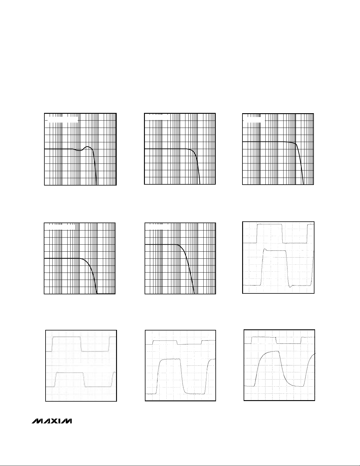
__________________________________________Typical Operating Characteristics
(VCC= +5V, VEE= -5V, SHDN = 0V, RL= 150Ω, TA = +25°C, unless otherwise noted.)
-5
-4
-3
-2
-1
0
1
2
3
4
5
100k 1M 10M 100M 1G
MAX4146
SMALL-SIGNAL GAIN
vs. FREQUENCY (A
V
= +100)
MAX4144/4146-04
FREQUENCY (Hz)
NORMALIZED GAIN (dB)
V
OUT
= 100mV
RMS
0.5
0.4
-0.5
100k 1M 10M 100M 1G
MAX4144
0.1dB GAIN FLATNESS vs.
FREQUENCY (A
V
= +2)
0
-0.1
-0.2
-0.3
-0.4
MAX444/46 TOC05
FREQUENCY (Hz)
NORMALIZED GAIN (dB)
0.1
0.2
0.3
V
OUT
= 100mV
RMS
5
-5
100k 1M
10M 100M 1G
MAX4144
SMALL-SIGNAL GAIN
vs. FREQUENCY (A
V
= +2)
-3
MAX4144/6 TOC-01
FREQUENCY (Hz)
NORMALIZED GAIN (dB)
-1
1
3
4
-4
-2
0
2
V
OUT
= 100mV
RMS
4
-6
100k 1M
10M 100M 1G
MAX4145
SMALL-SIGNAL GAIN
vs. FREQUENCY (A
V
= +1)
-4
MAX4144/6 TOC-02
FREQUENCY (Hz)
GAIN (dB)
-2
0
2
3
-5
-3
-1
1
V
OUT
= 100mV
RMS
5
-5
100k 1M
10M 100M 1G
MAX4146
SMALL-SIGNAL GAIN
vs. FREQUENCY (A
V
= +10)
-3
MAX4144/6 TOC-03
FREQUENCY (Hz)
NORMALIZED GAIN (dB)
-1
1
3
4
-4
-2
0
2
V
OUT
= 100mV
RMS
0.5
0.4
-0.5
100k 1M 10M 100M 1G
MAX4145
0.1dB GAIN FLATNESS vs.
FREQUENCY (A
V
= +1)
0
-0.1
-0.2
-0.3
-0.4
MAX4144/46 TOC06a
FREQUENCY (Hz)
NORMAILIZED GAIN (dB)
0.1
0.2
0.3
V
OUT
= 100mV
RMS
AC ELECTRICAL CHARACTERISTICS (continued)
(VCC= +5V, VEE= -5V, SHDN = 0V, RL= 150Ω, TA= T
MIN
to T
MAX
, unless otherwise noted. Typical values are at TA= +25°C.)
PARAMETER SYMBOL MIN TYP MAX UNITSCONDITIONS
0.03
0.06Differential Phase (Note 1) DP
0.07
Degrees
-66
-67
-48
f = 3.58MHz
f = 5MHz,
V
OUT
= 2Vp-p
MAX4144
MAX4145
MAX4146
Note 1: Differential gain and phase are tested using a modulated ramp, 100 IRE (0.714V).
-90
-92
Spurious-Free Dynamic Range SFDR
-82
dBc
f = 10kHz,
V
OUT
= 2Vp-p
MAX4144
MAX4145
MAX4146
AV= 2V/V
AV= 1V/V
AV= 10V/V
AV= 2V/V
AV= 1V/V
AV= 10V/V
MAX4144
MAX4145
MAX4146
MAX4144/MAX4145/MAX4146
High-Speed, Low-Distortion,
Differential Line Receivers
_______________________________________________________________________________________
5
-7
-6
-5
-4
-3
-2
-1
0
1
2
3
100k 1M 10M 100M 1G
MAX4146
LARGE-SIGNAL GAIN
vs. FREQUENCY (A
V
= +100)
MAX4144/4146-10
FREQUENCY (Hz)
NORMALIZED GAIN (dB)
V
OUT
= 2Vp-p
TIME (10ns/div)
MAX4144
SMALL-SIGNAL
PULSE RESPONSE (A
V
= +2)
IN
OUT
GND
GND
VOLTAGE (20mV/div)
TOC-11
GND
TIME (10ns/div)
GND
MAX4144/4146 TOC12
IN
OUT
VOLTAGE (50mV/div)
MAX4145
SMALL-SIGNAL
PULSE RESPONSE (A
V
= +1)
TIME (10ns/div)
MAX4146
SMALL-SIGNAL
PULSE RESPONSE (A
V
= +10)
IN
OUT
GND
GND
VOLTAGE (20mV/div)
TOC-13
TIME (10ns/div)
MAX4146
SMALL-SIGNAL
PULSE RESPONSE (A
V
= +100)
GND
GND
VOLTAGE
IN
OUT
1mV/div
20mV/div
TOC-14
_____________________________Typical Operating Characteristics (continued)
(VCC= +5V, VEE= -5V, SHDN = 0V, RL= 150Ω, TA = +25°C, unless otherwise noted.)
-5
-4
-3
-2
-1
0
1
2
3
4
5
100k 1M 10M 100M 1G
MAX4144
LARGE-SIGNAL GAIN
vs. FREQUENCY (A
V
= +2)
MAX4144/4146-07
FREQUENCY (Hz)
NORMALIZED GAIN (dB)
V
OUT
= 2Vp-p
4
3
-6
100k 1M 10M 100M 1G
MAX4145
LARGE-SIGNAL GAIN
vs. FREQUENCY (A
V
= +1)
-1
-2
-3
-4
-5
MAX4144/46 TOC-8
FREQUENCY (Hz)
NORMALIZED GAIN (dB)
0
1
2
V
OUT
= 2Vp-p
5
-5
100k 1M
10M 100M 1G
MAX4146
SMALL-SIGNAL GAIN
vs. FREQUENCY (A
V
= +10)
-3
MAX4144/6 TOC-09
FREQUENCY (Hz)
NORMALIZED GAIN (dB)
-1
1
3
4
-4
-2
0
2
V
OUT
= 100mV
RMS
0.5
0.4
-0.5
100k 1M 10M 100M 1G
MAX4146
0.1dB GAIN FLATNESS vs.
FREQUENCY (A
V
= +10)
0
-0.1
-0.2
-0.3
-0.4
MAX4144/46 TOC06
FREQUENCY (Hz)
NORMALIZED GAIN (dB)
0.1
0.2
0.3
V
OUT
= 100mV
RMS

MAX4144/MAX4145/MAX4146
High-Speed, Low-Distortion,
Differential Line Receivers
6 _______________________________________________________________________________________
_____________________________Typical Operating Characteristics (continued)
(VCC= +5V, VEE= -5V, SHDN = 0V, RL= 150Ω, TA = +25°C, unless otherwise noted.)
100
0.01
100k 1M 10M 100M 1G
CLOSED-LOOP OUTPUT IMPEDANCE
vs. FREQUENCY (A
V
= +1)
0.1
MAXXXXXX
FREQUENCY (Hz)
CLOSED-LOOP OUTPUT IMPEDANCE (Ω)
1
10
-0.01
0.01
0
-0.02
-0.03
-0.04
-0.01
0 100
0 100
MAX4144
DIFFERENTIAL GAIN AND PHASE
0.01
0
IRE
IRE
PHASE (deg)
GAIN (%)
0.04
0.03
0.02
MAX4144/6 TOC-20
AV = 2V/V
AV = 2V/V
0
0.05
-0.05
-0.10
-0.20
-0.15
-0.02
0 100
0 100
MAX4145
DIFFERENTIAL GAIN AND PHASE
0
IRE
IRE
PHASE (deg)
GAIN (%)
0.06
0.04
0.08
0.02
MAX4144/6 TOC-21
AV = 1V/V
AV = 1V/V
0
0.05
-0.05
-0.10
-0.15
-0.10
0 100
0
100
MAX4146
DIFFERENTIAL GAIN AND PHASE
-0.06
-0.08
IRE
IRE
PHASE (deg)
GAIN (%)
0
-0.02
0.02
-0.04
MAX4144/6 TOC-22
AV = 10V/V
AV = 10V/V
9.0
8.0
7.0
6.0
5.0
4.0
3.0
0 50 100 150 200 250
OUTPUT SWING
vs. LOAD RESISTANCE
MAX4144/4146-23
LOAD (Ω)
OUTPUT SWING (Vp-p)
MAX4144/46 TOC16
GND
TIME (10ns/div)
GND
IN
OUT
VOLTAGE (1V/div)
MAX4145
LARGE-SIGNAL
PULSE RESPONSE (A
V
= +1)
TIME (10ns/div)
MAX4146
LARGE-SIGNAL
PULSE RESPONSE (A
V
= +10)
IN
OUT
GND
GND
VOLTAGE (500mV/div)
TOC-17
TIME (10ns/div)
MAX4146
LARGE-SIGNAL
PULSE RESPONSE (A
V
= +100)
GND
GND
VOLTAGE
IN
(500mV/div)
(20mV/div)
OUT
TOC-18
TIME (10ns/div)
MAX4144
LARGE-SIGNAL
PULSE RESPONSE (A
V
= +2)
IN
OUT
GND
GND
VOLTAGE (500mV/div)
TOC-15

MAX4144/MAX4145/MAX4146
High-Speed, Low-Distortion,
Differential Line Receivers
_______________________________________________________________________________________
7
0
-100
100k 1M 10M 100M
MAX4146
HARMONIC DISTORTION
vs. FREQUENCY (A
V
= +10)
-80
MAX4144/4146 TOC-26
FREQUENCY (Hz)
DISTORTION (dBc)
-60
-40
-20
-10
-90
-70
-50
-30
V
OUT
= 2Vp-p
3RD HARMONIC
2ND HARMONIC
_____________________________Typical Operating Characteristics (continued)
(VCC= +5V, VEE= -5V, SHDN = 0V, RL= 150Ω, TA = +25°C, unless otherwise noted.)
0
-100
100k 1M 10M 100M
MAX4144
HARMONIC DISTORTION
vs. FREQUENCY (A
V
= +2)
-80
MAX4144/46/ TOC-24
FREQUENCY (Hz)
DISTORTION (dBc)
-60
-40
-20
-10
-90
-70
-50
-30
3RD HARMONIC
2ND HARMONIC
V
OUT
= 2Vp-p
0
-100
100k 1M 10M 100M
MAX4145
HARMONIC DISTORTION
vs. FREQUENCY (A
V
= +1)
-80
MAX4144/46 TOC25
FREQUENCY (Hz)
DISTORTION (dBc)
-60
-40
-20
-10
-90
-70
-50
-30
V
OUT
= 2Vp-p
3RD HARMONIC
2ND HARMONIC
0
-100
100k 1M 10M 100M
MAX4146
HARMONIC DISTORTION
vs. FREQUENCY (A
V
= +100)
-80
MAX4144/4146 TOC-27
FREQUENCY (Hz)
DISTORTION (dBc)
-60
-40
-20
-10
-90
-70
-50
-30
V
OUT
= 2Vp-p
3RD HARMONIC
2ND HARMONIC
0
-100
0 200 600 1k
MAX4144
5MHz HARMONIC DISTORTION
vs. LOAD (A
V
= +2)
-80
-20
MAX4144/4146-26
LOAD (Ω)
DISTORTION (dBc)
400 800
-40
-60
-90
-70
-10
-30
-50
2ND HARMONIC
3RD HARMONIC
V
OUT
= 2Vp-p
-100
-80
-90
-60
-70
-40
-50
-30
-10
-20
0
0 200 400 600 800 1k
MAX4145
5MHz HARMONIC DISTORTION
vs. LOAD (A
V
= +1)
MAX4145
LOAD (Ω)
DISTORTION (dBc)
V
OUT
= 2Vp-p
3RD HARMONIC
2ND HARMONIC
0
-100
0 200 600 1k
MAX4146
5MHz HARMONIC DISTORTION
vs. LOAD (A
V
= +10)
-80
-20
MAX4144/4146-30
LOAD (Ω)
DISTORTION (dBc)
400 800
-40
-60
-90
-70
-10
-30
-50
2ND HARMONIC
3RD HARMONIC
V
OUT
= 2Vp-p
0
-100
0 200 600 1k
MAX4146
5MHz HARMONIC DISTORTION
vs. LOAD (A
V
= +100)
-80
-20
MAX4144/4146-31
LOAD (Ω)
DISTORTION (dBc)
400 800
-40
-60
-90
-70
-10
-30
-50
2ND HARMONIC
3RD HARMONIC
V
OUT
= 2Vp-p
-100
-70
-80
-90
-60
-50
-40
-30
-20
-10
0
0.5 1.51.0 2.0 2.5 3.0 3.5
MAX4144
5MHz HARMONIC DISTORTION
vs. OUTPUT SWING (A
V
= +2)
MAX4144/46 TOC-32
VOLTAGE SWING (Vp-p)
DISTORTION (dBc)
2ND HARMONIC
3RD HARMONIC

MAX4144/MAX4145/MAX4146
High-Speed, Low-Distortion,
Differential Line Receivers
8 _______________________________________________________________________________________
_____________________________Typical Operating Characteristics (continued)
(VCC= +5V, VEE= -5V, SHDN = 0V, RL= 150Ω, TA = +25°C, unless otherwise noted.)
-100
-70
-80
-90
-60
-50
-40
-30
-20
-10
0
0.5 1.51.0 2.0 2.5 3.0 3.5
MAX4146
5MHz HARMONIC DISTORTION
vs. OUTPUT SWING (A
V
= +10)
MAX4144/4146 TOC-34
OUTPUT SWING (Vp-p)
DISTORTION (dBc)
3RD HARMONIC
2ND HARMONIC
-100
-70
-80
-90
-60
-50
-40
-30
-20
-10
0
0.5 1.51.0 2.0 2.5 3.0 3.5
MAX4146
5MHz HARMONIC DISTORTION
vs. OUTPUT SWING (A
V
= +100)
MAX4144/46 TOC35
OUTPUT SWING (Vp-p)
DISTORTION (dBc)
3RD HARMONIC
2ND HARMONIC
1
10 100 1k 10k 100k 1M
MAX4144
VOLTAGE NOISE DENSITY
vs. FREQUENCY (A
V
= +2)
10
100
MAX4144/4146-36
FREQUENCY (Hz)
VOLTAGE NOISE (nV/√Hz)
10 1k 10k 100k100 1M
MAX4145
VOLTAGE NOISE DENSITY
vs. FREQUENCY (A
V
= +1)
MAX4144/46 TOC-37
FREQUENCY (Hz)
VOLTAGE NOISE (nV/√Hz)
1000
10
100
1
10 100 1k 10k 100k 1M
MAX4146
VOLTAGE NOISE DENSITY
vs. FREQUENCY (A
V
= +10)
10
100
MAX4144/46-TOC38
FREQUENCY (Hz)
VOLTAGE NOISE (nV/√Hz)
10 1k 10k 100k100 1M
MAX4145
CURRENT NOISE DENSITY
vs. FREQUENCY (A
V
= +1)
MAX4144/46 TOC41Q
FREQUENCY (Hz)
CURRENT NOISE (pA/√Hz)
100
1
10
10 1k 10k 100k100 1M
MAX4144
CURRENT NOISE DENSITY
vs. FREQUENCY (A
V
= +2)
MAX4144/4146 TOC-40
FREQUENCY (Hz)
CURRENT NOISE (pA/√Hz)
10
0.1
1
1
10 100 1k 10k 100k 1M
MAX4146
VOLTAGE NOISE DENSITY
vs. FREQUENCY (A
V
= +100)
10
100
MAX4144/4146-39
FREQUENCY (Hz)
VOLTAGE NOISE (nV/√Hz)
-100
-80
-90
-60
-70
-40
-50
-30
-10
-20
0
0.5 1.5 2.01.0 2.5 3.0 3.5 4.0
MAX4145
5MHz HARMONIC DISTORTION
vs. OUTPUT SWING (A
V
= +1)
MAX4145
OUTPUT SWING (Vp-p)
DISTORTION (dBc)
3RD HARMONIC
2ND HARMONIC

MAX4144/MAX4145/MAX4146
High-Speed, Low-Distortion,
Differential Line Receivers
_______________________________________________________________________________________
9
110
10
100k 1M
10M 100M
MAX4144
COMMON-MODE REJECTION
vs. FREQUENCY (A
V
= +1)
30
MAX4144/6 TOC-43
FREQUENCY (Hz)
CMR (dB)
50
70
90
100
20
40
60
80
VCM = 100mV
RMS
25
35
45
55
65
75
85
95
105
115
125
100k 1M 10M 100M
POWER-SUPPLY REJECTION
vs. FREQUENCY
MAX4144/4146-42
FREQUENCY (Hz)
PSR (dB)
10 1k 10k 100k100 1M
MAX4146
CURRENT NOISE DENSITY
vs. FREQUENCY (A
V
= +10)
MAX4144/46 TOC41R
FREQUENCY (Hz)
CURRENT NOISE (pA/√Hz)
10
0.1
1
110
10
100k 1M
10M 100M
MAX4146
COMMON-MODE REJECTION
vs. FREQUENCY (A
V
= +10)
30
MAX4144/6 TOC-45
FREQUENCY (Hz)
CMR (dB)
50
70
90
100
20
40
60
80
VCM = 100mV
RMS
110
10
100k 1M 10M 100M
MAX4145
COMMON-MODE REJECTION
vs. FREQUENCY (A
V
= +2)
30
20
MAX4144/46 TOC44
FREQUENCY (Hz)
CMR (dB)
60
50
40
100
90
80
70
VCM = 100mV
RMS
TIME (20µs/div)
SHUTDOWN RESPONSE TIME
MAX4144/6 TOC-45
VOLTAGE
(1.V/div)
SHDN
OUT
GND
GND
(2.5V/div)
_____________________________Typical Operating Characteristics (continued)
(VCC= +5V, VEE= -5V, SHDN = 0V, RL= 150Ω, TA = +25°C, unless otherwise noted.)
10 1k 10k 100k100 1M
MAX4146
CURRENT NOISE DENSITY
vs. FREQUENCY (A
V
= +100)
MAX4144/46 TOC41
FREQUENCY (Hz)
CURRENT NOISE (pA/√Hz)
10
0.1
1

MAX4144/MAX4145/MAX4146
High-Speed, Low-Distortion,
Differential Line Receivers
10 ______________________________________________________________________________________
Pin Description
________________Detailed Description
The MAX4144/MAX4145/MAX4146 are low-distortion,
differential line receivers that feature high bandwidths
and excellent common-mode rejection, making them
ideal for balanced, high-speed data transmission systems.
The MAX4144 has a preset gain of +2V/V and achieves
a 130MHz -3dB bandwidth, a 1000V/µs slew rate, and
common-mode rejection (CMR) of 70dB at 10MHz. The
MAX4145 and MAX4146 use a single external resistor to
set the closed-loop gain from +1V/V to +10V/V for the
MAX4145, or greater than +10V/V for the MAX4146. The
MAX4145 achieves a -3dB bandwidth of 180MHz, a
slew rate of 600V/µs, and CMR of 75dB at 10MHz when
operating in the unity-gain configuration. The MAX4146
attains a -3dB bandwidth of 70MHz, a slew rate of
800V/µs, and CMR of 90dB at 10MHz when operating
with a closed-loop gain of +10V/V.
Differential inputs make the MAX4144/MAX4145/
MAX4146 ideal for applications with high common-
mode noise, such as receiving T1 or xDSL transmissions over a twisted-pair cable. Excellent differential
gain and phase, along with low noise, also suit them to
video applications and RF signal processing.
For a complete differential transmission link, use the
MAX4144/MAX4145/MAX4146 amplifiers with the
MAX4147 line driver, as shown in the
Typical Applica-
tion Circuit.
___________Applications Information
Grounding, Bypassing,
and PC Board Layout
Adhere to the following high-frequency design techniques when designing the PC board for the
MAX4144/MAX4145/MAX4146.
• The printed circuit board should have at least two
layers: the signal layer and the ground plane.
• Do not use wire-wrap boards—they are too
inductive.
FUNCTIONNAME
9
11
13
4
5
6
8, 14
3
10, 12
2
1, 7
PIN
Output Reference. Connect to ground for
normal operation.
REF9
OutputOUT11
Output Sense. Connect to OUT close to
the pin for normal operation.
SENSE13
Logic Input for Shutdown Circuitry. A logic
low enables the amplifier. A logic high
disables the amplifier.
SHDN4
Noninverting Input for Gain-Set Resistor RG+—
Noninverting InputIN+6
Positive Power SupplyV
CC
8, 14
Inverting Input for Gain-Set ResistorRG-—
No Connect. Not internally connected.N.C.
3, 5, 10,
12
Inverting InputIN-2
Negative Power SupplyV
EE
1, 7
9
11
13
4
5
6
8, 14
3
10, 12
2
1, 7
MAX4146MAX4144 MAX4145
14 SO14 SO 14 SO16 QSOP 16 QSOP 16 QSOP
1, 7
2
3, 5, 8, 9,
12,14
1, 7
2
12, 14
1, 7
2
12, 14
3 3—
4 4 4
— 5 5
6 6 6
10, 16 10, 16 10, 16
11 11 11
13 13 13
15 15 15

MAX4144/MAX4145/MAX4146
High-Speed, Low-Distortion,
Differential Line Receivers
______________________________________________________________________________________ 11
• Do not use IC sockets—they increase parasitic
capacitance and inductance.
• Use surface-mount power-supply bypass capacitors
instead of through-hole capacitors. Their shorter
lead lengths reduce parasitic inductance, leading to
superior high-frequency performance.
• Keep signal lines as short and as straight as possible. Do not make 90° turns; round all corners.
• The ground plane should be as free from voids as
possible.
Output Short-Circuit Protection
Under short-circuit conditions to ground, limit the output current to 120mA. This level is low enough that a
short to ground of moderate duration will not cause permanent damage to the chip. However, a short to either
supply will significantly increase power dissipation, and
will cause permanent damage. The high output current
capability is an advantage in systems that transmit a
signal to several loads.
Input Protection Circuitry
The MAX4144/MAX4145/MAX4146 include internal protection circuitry that prevents damage to the precision
input stage from large differential input voltages. This
protection circuitry consists of five back-to-back
Schottky protection diodes between IN+ and RG+, and
IN- and RG- (Figure 1). The diodes limit the differential
voltage applied to the amplifiers’ internal circuitry to no
more than 10VF, where VFis the diode’s forward voltage drop (about 0.4V at +25°C).
For a large differential input voltage (exceeding 4V), the
MAX4145/MAX4146 input bias current (at IN+ and IN-)
increases according to the following equation:
The MAX4144 has an internal gain-setting resistor valued at 1.4kΩ. A differential input voltage as high as 10V
will cause only 4.3mA to flow—much less than the
10mA absolute maximum rating. However, in the
MAX4145/MAX4146, R
G
can be as low as 150Ω. Under
this condition, the absolute maximum input current rating might be exceeded if the differential input voltage
exceeds 5.5V (10mA x 150Ω + 10VF). In that case,
510Ω resistors can be placed at IN+ and IN- to limit the
current without degrading performance.
Shutdown Mode
The MAX4144/MAX4145/MAX4146 can be put into lowpower shutdown mode by bringing SHDN high. The
amplifier output is high impedance in this mode; thus
the impedance at OUT is that of the feedback resistors
(1.4kΩ).
Setting Gain (MAX4145/MAX4146)
The MAX4145/MAX4146 ’s gain is determined by a single external resistor, RG. The optimal gain range is from
+1V/V to +10V/V for the MAX4145 and +10V/V (RG=
open) to +100V/V for the MAX4146. The gain (in V/V) is
given in the following equations:
Input Current=
V - V - 10V
R
IN+ IN- F
G
( )
1.4k
IN+
IN-
IN+
IN-
R
G
-
R
G
+
MAX4144 MAX4145
MAX4146
Figure 1. Input Protection Circuits

MAX4144/MAX4145/MAX4146
High-Speed, Low-Distortion,
Differential Line Receivers
12 ______________________________________________________________________________________
Figure 2 shows the connection for RG. RGmight simply
be a resistor, or it can be a complex pole-zero pair for
filter and shaping applications (Figure 9). Use surfacemount gain-setting components to ensure stability.
Using REF and SENSE
The MAX4144/MAX4145/MAX4146 have a REF pin (normally connected to ground) and a SENSE pin (normally
connected to OUT). In some long-line applications, it
may be desirable to connect SENSE and OUT together
at the load, instead of the typical connection at the part
(Figure 3). This compensates for the long line’s resistance, which otherwise leads to an IR voltage error.
When using this technique, keep the sense lines’
impedance low to minimize gain errors. Also, keep
capacitance low to maximize frequency response. The
gain of the MAX4144/MAX4145/MAX4146 output stage
is approximated by the following equation:
where ∆R
SENSE
and ∆R
REF
are the SENSE and REF
trace impedances, respectively. R is 700Ω for the
MAX4144 and MAX4145, and 100Ω for the MAX4146.
Additionally, mismatches in the SENSE and REF traces
lead to common-mode gain errors. Common-mode
gain is approximated by the following equation:
Substituting numbers for ∆R
REF
and ∆R
SENSE
into this
equation, we can see that if changes in ∆R
REF
and
∆R
SENSE
are equal, CMR is not degraded.
Driving Capacitive Loads
The MAX4144/MAX4145/MAX4146 provide maximum
AC performance when not driving an output load
capacitance. This is the case when driving a correctly
terminated transmission line (i.e., a back-terminated
cable). In most amplifier circuits, driving large load
capacitance increases the chance of oscillations. The
amplifier’s output impedance and the load capacitor
combine to add a pole and excess phase to the loop
response. If the pole’s frequency is low enough and
phase margin is degraded sufficiently, oscillations may
occur. A second concern when driving capacitive
loads results from the amplifier’s output impedance,
A =
R - R
R + 700
VCM
REF SENSE
∆ ∆
Ω
700 R
R 700 R
REF
REF
Ω ∆
Ω ∆
+
+
+ +
A =
12700 R
R
1
700 R
R 700 R
V
SENSE REF
REF
Ω ∆ Ω ∆
Ω ∆
+
+
+
+ +
G = A = 1 +
1.4k
R
(MAX4145)
G = A = 10 +
14k
R
(MAX4146)
V
G
V
G
Ω
Ω
100k 1M 10M 100M 1G
-3
-4
-5
-2
FREQUENCY (Hz)
GAIN (dB)
-1
0
1
2
3
4
5
CL = 10pF
CL = 5pF
CL = 15pF
Figure 4. MAX4144 Small-Signal Response with Capacitive
Load
SENSE
OUT
REF
R
L
MAX4144
MAX4145
MAX4146
Figure 3. Connection of SENSE and REF to a Remote Load
IN-
R
G
IN+
MAX4145
MAX4146
Figure 2. Connection of RGin MAX4146

MAX4144/MAX4145/MAX4146
High-Speed, Low-Distortion,
Differential Line Receivers
______________________________________________________________________________________ 13
which appears inductive at high frequencies. This
inductance forms an L-C resonant circuit with the
capacitive load, which causes peaking in the frequency
response and degrades the amplifier’s phase margin.
The MAX4144/MAX4145/MAX4146 drive capacitive
loads up to 25pF without oscillation. However, some
peaking may occur in the frequency domain (Figure 4).
To drive larger capacitance and reduce ringing, add an
isolation resistor (R
ISO
) between the amplifier’s output
and the load (Figure 5).
The value of R
ISO
depends on the circuit’s gain and the
capacitive load (Figures 6 and 7). With higher capaci-
tive values, bandwidth is dominated by the RC network
formed by R
ISO
and CL; the bandwidth of the amplifier
itself is much higher. Also note that the isolation resistor
forms a divider that decreases the voltage delivered to
the load.
Twisted-Pair Line Receiver
The MAX4144/MAX4145/MAX4146 are well suited as
receivers in twisted-pair xDSL or NTSC/PAL video
applications. The standard 24AWG telephone wire
widely used in these applications is a lossy medium for
high-frequency signals. The losses in NTSC video
applications are almost 15dB per 1000 feet (Figure 8).
4
0
8
6
CAPACITIVE LOAD (pF)
ISOLATION RESISTANCE (Ω)
200
16
18
12
10
14
50 150 250
20
100
AV = 10V/V
Figure 6. MAX4144 Isolation Resistance vs. Capacitve Load
0
0
5
CAPACITIVE LOAD (pF)
ISOLATION RESISTANCE (Ω)
200
25
15
10
20
50 150 250
30
100
Figure 7. MAX4145/MAX4146 Isolation Resistance vs.
Capacitive Load
R
LOAD
C
LOAD
R
ISO
OUT
MAX4144
MAX4145
MAX4146
Figure 5. Addition of R
ISO
to Amplifier Output
15
-35
-30
-25
10k 1M 10M
-20
-15
-10
-5
0
5
10
100k
FREQUENCY (Hz)
GAIN (dB)
Figure 8. 1000 Feet of AWG24 Twisted-Pair Telephone Cable
(Gain vs. Frequency)

MAX4144/MAX4145/MAX4146
High-Speed, Low-Distortion,
Differential Line Receivers
14 ______________________________________________________________________________________
TWISTED-PAIR-TO-COAX CABLE CONVERTER
Losses are higher at higher frequencies, contributing to
severe pulse-edge rounding in digital applications. The
nominal impedance of twisted-pair telephone wire is
110Ω.
The MAX4145/MAX4146, with variable gain up to
+10V/V and +100V/V, respectively, can be used to
compensate for cable losses. In the graph shown in
Figure 8, the cable characteristics are such that the
video-chroma frequency loss is almost 15dB greater
than the low-frequency loss. The losses can be compensated for by using the RC-shaping network (Figure
9).
A 560Ω resistance and a 100pF capacitance shape the
MAX4146 gain to inversely match the frequency of the
1000 feet of telephone cable. The differential gain and
phase, using the circuit shown in Figure 9, is 0.55%
and 0.18°, respectively.
Figure 9. Circuit for Transmitting NTSC/PAL Video Over 1000 Feet of Twisted-Pair Telephone Line
VIDEO INPUT
VIDEO
OUTPUT
75Ω
75Ω
1, 7
8, 14
10
12
9
13
1000 FEET
2
6
MAX4147ESD
0.1µF
V
CC
0.1µF
V
EE
0.1µF
11
9
13
75Ω
2
110Ω
560Ω
100pF
6
5
3
V
CC
V
EE
MAX4146ESD
0.1µF
1, 7
8, 14
__________________________________________________Typical Application Circuit
R
R
T
T
IN-
IN+
SENSE
MAX4144
REF
75Ω
OUT
75Ω
COAX
75Ω
R
IN+
IN-
SENSE+
MAX4147
SENSE-
OUT+
OUT-
T
R
T
V
OUT

MAX4144/MAX4145/MAX4146
High-Speed, Low-Distortion,
Differential Line Receivers
______________________________________________________________________________________ 15
___________________Chip Information
TRANSISTOR COUNT: 237
SUBSTRATE CONNECTED TO V
EE
Pin Configurations
14
13
12
11
10
9
8
1
2
3
4
5
6
7
V
CC
SENSE
N.C.
OUT
SHDN
N.C.
IN-
V
EE
TOP VIEW
MAX4144
N.C.
REF
V
CC
V
EE
IN+
N.C.
SO
R
F
R R
SENSE
R
REF
R
R
F
R
G
14
13
12
11
10
9
8
1
2
3
4
5
6
7
V
CC
SENSE
N.C.
OUT
SHDN
RG-
IN-
V
EE
MAX4145
MAX4146
N.C.
REF
V
CC
V
EE
IN+
RG+
R
F
R R
SENSE
R
REF
R
R
F
SO
16
15
14
13
12
11
10
1
2
3
4
5
6
7
V
CC
SENSE
N.C.
OUT
SHDN
N.C.
IN-
V
EE
MAX4144
N.C.
REF
V
CC
V
EE
IN+
9
8
N.C
N.C.
N.C.
QSOP
R
F
R R
SENSE
R
REF
R
R
F
R
G
16
15
14
13
12
11
10
1
2
3
4
5
6
7
V
CC
SENSE
N.C.
OUT
SHDN
RG-
IN-
V
EE
MAX4145
MAX4146
N.C.
REF
V
CC
V
EE
9
8
N.C.
N.C.
IN+
RG+
R
F
R R
SENSE
R
REF
R
R
F
QSOP

Maxim cannot assume responsibility for use of any circuitry other than circuitry entirely embodied in a Maxim product. No circuit patent licenses are
implied. Maxim reserves the right to change the circuitry and specifications without notice at any time.
16
____________________Maxim Integrated Products, 120 San Gabriel Drive, Sunnyvale, CA 94086 408-737-7600
© 1998 Maxim Integrated Products Printed USA is a registered trademark of Maxim Integrated Products.
MAX4144/MAX4145/MAX4146
High-Speed, Low-Distortion,
Differential Line Receivers
________________________________________________________Package Information
SOICN.EPS
QSOP.EPS
 Loading...