

EVALUATION KIT
AVAILABLE
For free samples & the latest literature: http://www.maxim-ic.com, or phone 1-800-998-8800.
For small orders, phone 408-737-7600 ext. 3468.
General Description
The MAX4142 differential line driver combines highspeed performance with fully symmetrical differential
inputs and outputs. With an internally set +2V/V closedloop gain, the MAX4142 is ideal for driving backterminated cables and transmission lines.
This device utilizes laser-trimmed thin-film resistors and
common-mode cancellation circuitry to deliver an outstanding 67dB at 10MHz common-mode rejection
(CMR). Using current-feedback techniques, the
MAX4142 achieves a 250MHz -3dB (AV= +2V/V) bandwidth, a 70MHz 0.1dB bandwidth, and a 1400V/µs slew
rate. Excellent differential gain/phase error and noise
specifications make this amplifier an excellent choice
for a wide variety of video and RF signal-processing
applications.
The MAX4142 operates from ±5V power supplies and
requires only 12.5mA of quiescent current. The output
stage is capable of driving a 100Ω load to ±6V (differentially) or to ±3V (single-ended). The MAX4142 is
available in a space-saving 14-pin SO package. For a
pin-compatible, higher speed differential line driver,
see the MAX4147 data sheet.
________________________Applications
Video Twisted-Pair Driver
Differential Pulse Amplifier
High-Speed Instrumentation Amplifier
Low-Noise Differential Receivers
Differential ADC Driver
____________________________Features
♦ 250MHz -3dB Bandwidth (AV= +2V/V)
♦ 1400V/µs Slew Rate
♦ 67dB at 10MHz CMR
♦ 0.01%/0.01° Differential Gain/Phase
♦ ±6V Differentially into 100Ω Output Drive
♦ 1mA Shutdown Capability
♦ 12.5mA Quiescent Supply Current
♦ Available in 14-Pin Narrow SO Package
MAX4142
250MHz, Low-Power,
High-Output-Current, Differential Line Driver
________________________________________________________________
Maxim Integrated Products
1
GND
OUT+
IN+
IN-
IN-
SENSE
IN+
OUT-
SENSE-
SENSE+
R
t
R
t
R
t
R
t
OUT
REF
75Ω
75Ω
COAX
75Ω
V
OUT
MAX4142
MAX4144
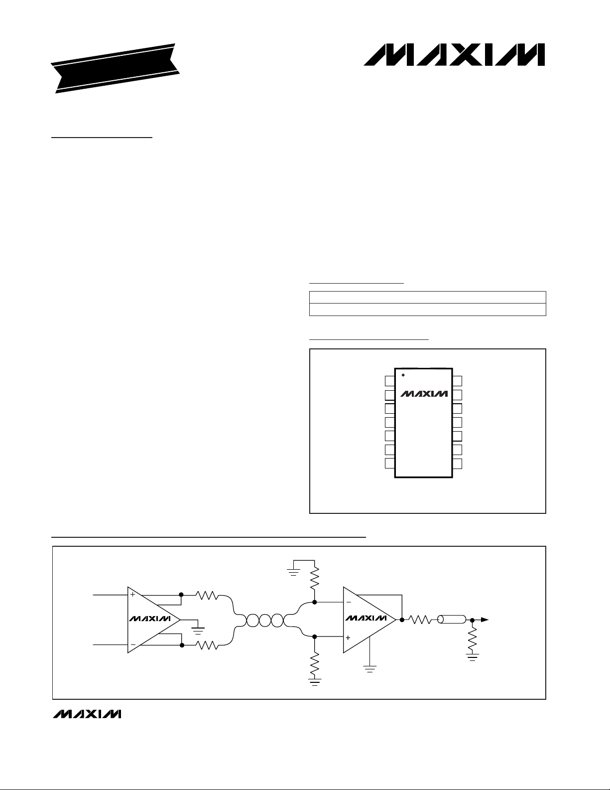
Typical Application Circuit
19-4763; Rev 0; 7/98
Ordering Information
TWISTED-PAIR TO COAX-CABLE CONVERTER
PART
MAX4142ESD
TEMP. RANGE
-40°C to +85°C
PIN-PACKAGE
14 SO
Pin Configuration
14
13
12
11
10
9
8
1
2
3
4
5
6
7
V
CC
OUT+
SENSE+
GND
SHDN
N.C.
IN+
V
EE
TOP VIEW
MAX4142
SENSEOUTV
CC
V
EE
IN-
N.C.
SO
N.C. = NOT INTERNALLY CONNECTED
MAX4142
250MHz, Low-Power, High-Output-Current,
Differential Line Driver
2 _______________________________________________________________________________________
ABSOLUTE MAXIMUM RATINGS
DC ELECTRICAL CHARACTERISTICS
(VCC= +5V, VEE= -5V, SHDN = 0, RL= ∞, TA= T
MIN
to T
MAX
, unless otherwise noted. Typical values specified at TA= +25°C.)
Stresses beyond those listed under “Absolute Maximum Ratings” may cause permanent damage to the device. These are stress ratings only, and functional
operation of the device at these or any other conditions beyond those indicated in the operational sections of the specifications is not implied. Exposure to
absolute maximum rating conditions for extended periods may affect device reliability.
Supply Voltage (VCCto VEE)................................................+12V
Voltage on Any Pin to Ground..........(V
EE
- 0.3V) to (VCC+ 0.3V)
Input Current (IN_)............................................................±10mA
Short-Circuit Duration (V
OUT
to GND)................................10sec
Continuous Power Dissipation (T
A
= +70°C)
Plastic SO (derate 8.3mW/°C above +70°C) ................667mW
Operating Temperature Range ...........................-40°C to +85°C
Storage Temperature Range.............................-65°C to +150°C
Lead Temperature (soldering, 10sec).............................+300°C
Differential Input Voltage Range -3.0 3.0 VGuaranteed by output voltage swing test
SHDN Input Current I
SHDN
66 150 µAV
SHDN
= 0
Output Resistance R
OUT
0.1 Ω
SHDN Logic-High Threshold V
IH
2.0 V
SHDN Logic-Low Threshold V
IL
0.8 V
Enable Time from Shutdown t
ON
500 ns
Disable Time to Shutdown t
OFF
3.5 µs
PARAMETER SYMBOL MIN TYP MAX UNITS
Input Offset Current I
OS
0.2 2.5 µA
Input Bias Current I
B
10 25 µA
Input Capacitance C
IN
1 pF
Differential Input Resistance R
IN
1 MΩ
Input Offset Voltage
Operating Supply Voltage ±4.5 ±5.5 V
V
OS
0.4 8 mV
Input Offset Voltage Drift TC
VOS
3 µV/°C
Common-Mode Input Voltage Range V
CM
-1.7 1.7 V
Gain A
V
2 V/V
Gain Error 0.3 2 %
Gain Drift 20 ppm/°C
Common-Mode Rejection CMR 55 80 dB
Power-Supply Rejection PSR 65 95 dB
Quiescent Supply Current I
CC, IEE
12.5 18 mA
Shutdown Supply Current I
CC, SHDN
1.0 2.0 mA
3.0 3.4
6.0 6.8
2.0 2.4
Output Voltage Swing
V
OUT
4.0 4.8
V
Output Current Drive I
OUT
120 75 mA
CONDITIONS
Guaranteed by CMR test
-1V ≤ V
OUT
≤ 1V, RL= 53Ω
V
IN
= 0
V
IN
= 0
-1V ≤ V
OUT
≤ 1V, RL= 53Ω
RL= 53Ω
VCM= ±1.7V
VS= ±4.5V to ±5.5V
VIN= 0
Guaranteed by PSR test
V
SHDN
≥ 2V, VIN= 0
V
IN
= 0
Single-ended, RL= ∞
Differential, RL= ∞
V
IN
= 0
Single-ended, RL= 26.5Ω
Differential, RL= 53Ω
RL= 20Ω
MAX4142
250MHz, Low-Power, High-Output-Current,
Differential Line Driver
_______________________________________________________________________________________ 3
AC ELECTRICAL CHARACTERISTICS
(VCC= +5V, VEE= -5V, SHDN = 0V, RL= 150Ω differential, TA= T
MIN
to T
MAX
, unless otherwise noted. Typical values specified at
T
A
= +25°C.)
__________________________________________Typical Operating Characteristics
(VCC= +5V, VEE= -5V, SHDN = 0, RL= 150Ω differential, TA = +25°C, unless otherwise noted.)
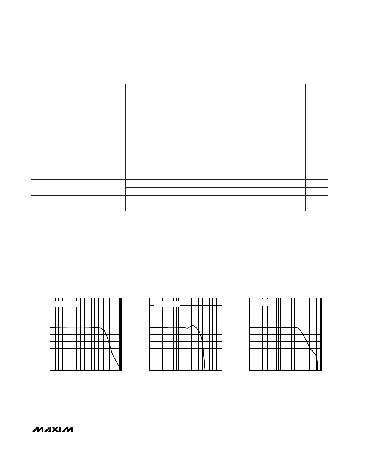
10
0
0.1 10 10001 100
SMALL-SIGNAL GAIN
vs. FREQUENCY
2
MAX4142-01
FREQUENCY (MHz)
GAIN (dB)
4
6
8
9
1
3
5
7
V
OUT
= 100mVp-p
6.4
5.4
0.1 10 10001 100
GAIN FLATNESS vs. FREQUENCY
5.6
MAX4142-02
FREQUENCY (MHz)
GAIN (dB)
5.8
6.0
6.2
6.3
5.5
5.7
5.9
6.1
V
OUT
= 100mVp-p
10
0
0.1 10 10001 100
LARGE-SIGNAL GAIN
vs. FREQUENCY
2
MAX4142-03
FREQUENCY (MHz)
GAIN (dB)
4
6
8
9
1
3
5
7
V
OUT
= 2Vp-p
to 0.01%
to 0.1%
PARAMETER SYMBOL MIN TYP MAX UNITS
Settling Time t
S
45
25
ns
Slew Rate SR 1400 V/µs
Common-Mode Rejection CMR 67 dB
Differential Gain DG 0.01 %
Differential Phase DP 0.01 degrees
2
Input Current Noise i
n
20
pA√Hz
Full-Power Bandwidth
-3dB Bandwidth BW
(-3dB)
250 MHz
FPBW 180 MHz
0.1dB Bandwidth BW
(0.1dB)
70 MHz
CONDITIONS
-1V ≤ V
OUT
≤ +1V
Differential, -2V ≤ V
OUT
≤ +2V
f = 10MHz, VCM= ±2V
f = 3.58MHz
f = 3.58MHz
f = 10kHz
f = 1MHz to 100MHz
V
OUT
≤ 0.1V
RMS
V
OUT
= 2Vp-p
V
OUT
≤ 0.1V
RMS
-84
Spurious-Free Dynamic
Range
SFDR
-76
dBc
fC= 500kHz, V
OUT
= 1Vp-p, RS= 50Ω, Figure1
fC= 10MHz, V
OUT
= 1Vp-p, RS= 50Ω, Figure1
8
Input Voltage Noise e
n
80
nV/√Hz
f = 10kHz
f = 1MHz to 100MHz µV
RMS
nA
RMS
MAX4142
250MHz, Low-Power, High-Output-Current,
Differential Line Driver
4 _______________________________________________________________________________________
_____________________________Typical Operating Characteristics (continued)
(VCC= +5V, VEE= -5V, SHDN = 0, RL= 150Ω differential, TA = +25°C, unless otherwise noted.)
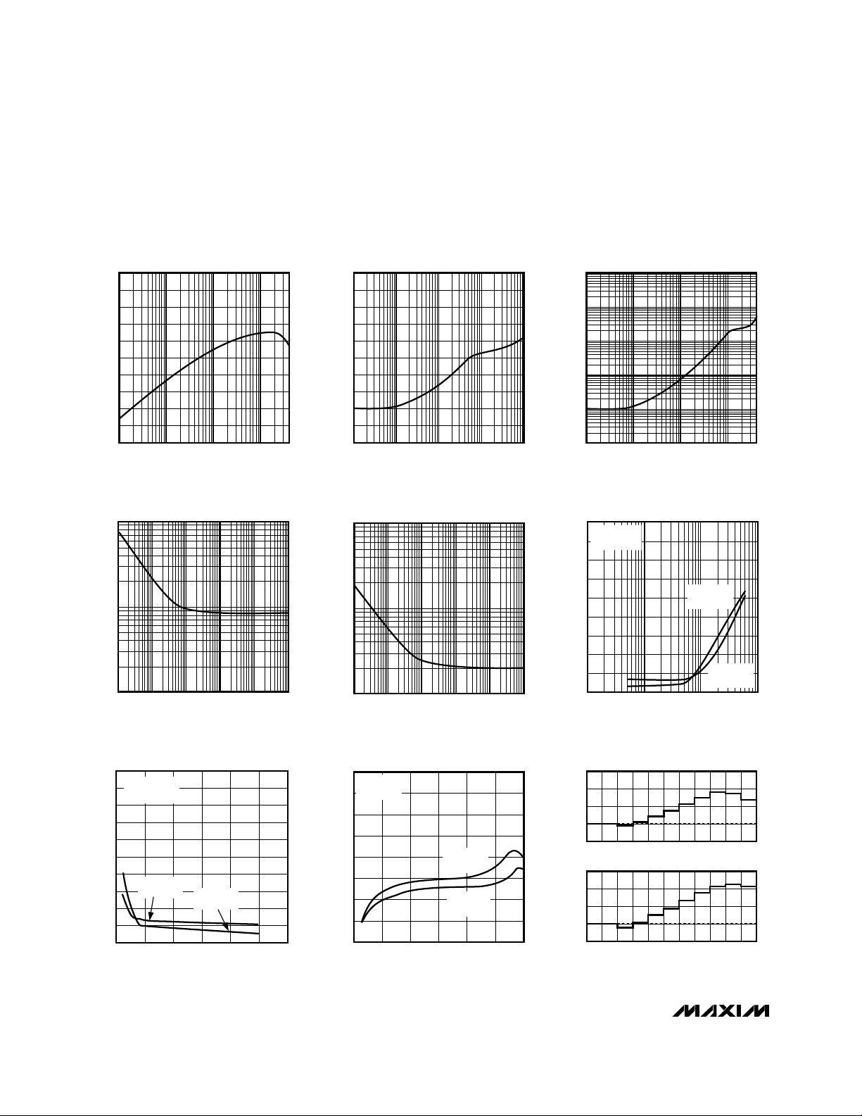
10
110
0.1 101 100
POWER-SUPPLY REJECTION
vs. FREQUENCY
90
MAX4142-04
FREQUENCY (MHz)
PSR (dB)
70
50
30
20
100
80
60
40
-10
90
0.1 10 10001 100
COMMON-MODE REJECTION
vs. FREQUENCY
70
MAX4142-05
FREQUENCY (MHz)
CMR (dB)
50
30
10
0
80
60
40
20
0.01
0.1
1
10
100
1000
0.1 101 100
OUTPUT IMPEDANCE vs. FREQUENCY
MAX4142-06
FREQUENCY (MHz)
OUTPUT IMPEDANCE (Ω)
1
10
100
10 100 1k 10k 100k 1M
VOLTAGE-NOISE DENSITY
vs. FREQUENCY
MAX4142-07
FREQUENCY (Hz)
VOLTAGE-NOISE DENSITY (nV/√
Hz
)
-100
-90
-60
-80
-70
-50
-30
-40
-20
0 400200 600 800 1000 1200
DISTORTION vs. LOAD
MAX4142-10
RESISTIVE LOAD (Ω)
DISTORTION (dBc)
2nd ORDER
HARMONIC
3rd ORDER
HARMONIC
fO = 5MHz,
V
OUT
= 1Vp-p
1
10
100
10 100 1k 10k 100k 1M
CURRENT-NOISE DENSITY
vs. FREQUENCY
MAX4142-08
FREQUENCY (Hz)
CURRENT-NOISE DENSITY (pA/√
Hz
)
0.1 1 10 100
HARMONIC DISTORTION
vs. FREQUENCY
MAX4142-09
FREQUENCY (MHz)
DISTORTION (dBc)
-90
-70
-80
-40
-50
-60
-10
-20
-30
0
RL = 150Ω
V
OUT
= 1Vp-p
2nd
HARMONIC
3rd
HARMONIC
-100
-90
-80
-70
-60
-50
-40
-30
-20
0 42 6 8 10 12
HARMONIC DISTORTION
vs. OUTPUT VOLTAGE SWING
MAX4142-11
OUTPUT VOLTAGE SWING (Vp-p)
DISTORTION (dBc)
f = 5MHz
R
L
= 150Ω
2nd
HARMONIC
3rd
HARMONIC
-0.005
0 100
0 100
DIFFERENTIAL GAIN AND PHASE
-0.005
0.000
0.000
0.005
0.005
0.010
0.010
0.015
IRE
DIFF. PHASE (deg)
DIFF. GAIN (%)
MAX4142-12

MAX4142
250MHz, Low-Power, High-Output-Current,
Differential Line Driver
_______________________________________________________________________________________
5
0
4
2
8
6
10
12
16
14
18
0 100 200 300 400 500
DIFFERENTIAL OUTPUT SWING
vs. LOAD RESISTANCE
MAX4142-13
LOAD RESISTANCE (Ω)
OUTPUT SWING (Vp-p)
12
13
16
15
14
17
18
-45 -15-30 0 15 30 45 60 75 90
DIFFERENTIAL OUTPUT VOLTAGE
SWING vs. TEMPERATURE
MAX4142-14
TEMPERATURE (°C)
DIFFERENTIAL OUTPUT VOLTAGE SWING (V)
RL = 1MΩ DIFFERENTIAL
0
0.2
0.1
0.4
0.3
0.6
0.5
0.7
0.9
0.8
1
-45 -15 0 15-30 30 45 60 75 90
INPUT OFFSET VOLTAGE
vs. TEMPERATURE
MAX4142-15
TEMPERATURE (°C)
INPUT OFFSET VOLTAGE (mV))
5
9
7
15
13
11
19
17
-45 0 15-30 -15 30 45 60 75 90
INPUT BIAS CURRENT
vs. TEMPERATURE
MAX4142-16
TEMPERATURE (°C)
INPUT BIAS CURRENT (µA)
OUT
IN
GND
GND
TIME (10ns/div)
SMALL-SIGNAL PULSE RESPONSE
MAX4142-19
VOLTAGE (25mV/div)
0
0.2
0.1
0.4
0.3
0.6
0.5
0.7
0.9
0.8
1.0
-45 -15 0 15-30 30 45 60 75 90
INPUT OFFSET CURRENT
vs. TEMPERATURE
MAX4142-17
TEMPERATURE (°C)
INPUT OFFSET CURRENT (µA)
10.0
11.0
10.5
12.0
11.5
13.0
12.5
13.5
14.5
14.0
15.0
-45 -15 0 15-30 30 45 60 75 90
POWER-SUPPLY CURRENT
vs. TEMPERATURE
MAX4142-18
TEMPERATURE (°C)
POWER-SUPPLY CURRENT (mA)
OUT
IN
GND
GND
TIME (10ns/div)
LARGE-SIGNAL PULSE RESPONSE
MAX4142-20
VOLTAGE (500mV/div)
V
OUT
SHDN
0V
5V
0V
2V
TIME (2µs/div)
ENABLE RESPONSE TIME
MAX4142-21
_____________________________Typical Operating Characteristics (continued)
(VCC= +5V, VEE= -5V, SHDN = 0, RL= 150Ω differential, TA = +25°C, unless otherwise noted.)

MAX4142
250MHz, Low-Power, High-Output-Current,
Differential Line Driver
6 _______________________________________________________________________________________
Detailed Description
The MAX4142 differential line driver features 250MHz
bandwidth and 67dB common-mode rejection (CMR) at
10MHz. This part achieves a 1400V/µs slew rate, and
power dissipation is only 125mW. The MAX4142 has an
internally set +2V/V closed-loop gain, making it ideal as
a back-terminated line driver. The output stage can
drive ±6V into a 100Ω load.
The MAX4142 utilizes a three-amplifier topology to provide differential inputs/outputs and common-mode
feedback (Figure 1), making it ideal for applications
with high common-mode noise, such as for driving T1
or xDSL transmissions over a twisted-pair cable. The
MAX4142’s differential noninverting structure uses two
noninverting amplifiers (A1 and A2) to provide a single
device with differential inputs and outputs. The use of
two amplifiers effectively doubles the output voltage
swing and bandwidth, and improves slew rate when
compared to the single op-amp differential amplifier.
Excellent gain and phase, along with low noise, also
make the MAX4142 suitable for video applications and
RF-signal processing.
For a complete differential transmission link, use the
MAX4142 line driver with the MAX4144/MAX4146 line
receivers, as shown in the
Typical Application Circuit
.
Applications Information
Balanced Transmission Lines
Differential (balanced) transmission lines use two conductors to transmit high-speed signals over low-cost
cable or twisted-pair wire with minimal signal degradation. The transmit side of the balanced transmission line
is driven by an amplifier with differential outputs, while
the signal is received by an amplifier with differential
inputs. In an ideal balanced system, each conductor
has the same impedance from input to output and from
the conductor to the system ground. Since the impedance from each conductor to ground is equivalent, any
noise or other interference coupled into the transmission line will be equal in magnitude in each conductor,
appearing as a common-mode signal to the amplifier at
the receiving end of the transmission line. Since the
receiving amplifier subtracts the signals on each side
of the transmission line to obtain the desired information, common-mode signals are effectively canceled
out by the receiving amplifier.
Common-Mode Feedback
In nonideal balanced systems, impedance mismatches
between the conductors of a transmission line can
degrade system common-mode rejection (CMR) by
converting a portion of any common-mode signal to a
_____________________Pin Description
MAX4142
A1
OUT+
IN+
V
IN
IN-
SENSE+
GND
SENSE-
OUT-
A3
A2
R
F
R
F
R
G
R
G
R
F
R
G
V
OUT
= 1 + V
IN
( )
Figure 1. MAX4142 Functional Diagram
12 SENSE+
Noninverting Output Sense. Connect
to OUT+ close to the pin for normal
operation.
13 OUT+ Noninverting Output
11 GND Ground
6 IN- Inverting Input
9 OUT- Inverting Output
10 SENSE-
Inverting Output Sense. Connect to OUTclose to the pin for normal operation.
8, 14 V
CC
Positive Power Supply. Connect V
CC
to +5V.
3, 5 N.C. No Connect. Not internally connected.
4 SHDN
Logic Input for Shutdown Circuitry. A
logic low enables the amplifier. A logic
high disables the amplifier.
2 IN+ Noninverting Input
NAME FUNCTION
1, 7 V
EE
Negative Power Supply. Connect V
EE
to -5V.
PIN

MAX4142
250MHz, Low-Power, High-Output-Current,
Differential Line Driver
_______________________________________________________________________________________ 7
differential signal that is amplified by the receiver. The
unique topology of the MAX4142 (Figure 1) utilizes two
amplifiers (A1 and A2) to provide differential inputs and
outputs, and a third amplifier (A3) to provide commonmode feedback. The common-mode feedback amplifier senses common-mode voltage at the MAX4142
output and forces this voltage to zero, effectively
removing common-mode voltages from the transmission line. This technique improves CMR for systems
with imperfectly balanced transmission-line impedances.
Grounding, Bypassing,
and PC Board Layout
Observe the following guidelines when designing your
PC board:
• High-frequency design techniques must be followed
when designing the PC board for the MAX4142.
• The printed circuit board should have at least two
layers: the signal layer and the ground plane.
• Do not use wire-wrap boards; they are too inductive.
• Do not use IC sockets; they increase parasitic
capacitance and inductance.
• Use surface-mount power-supply bypass capacitors
instead of through-hole capacitors. Their shorter lead
lengths reduce parasitic inductance, leading to
superior high-frequency performance.
• Keep signal lines as short and as straight as possible. Do not make 90° turns; round all corners.
• The ground plane should be as free from voids as
possible.
Input Stage Circuitry
The MAX4142 includes internal protection circuitry that
prevents damage to the precision input stage from
large differential input voltages. This protection circuitry
consists of five back-to-back Schottky protection
diodes between IN+ and RG, and IN- and RG(Figure 2). The diodes limit the differential voltage applied
to the amplifiers’ internal circuitry to no more than 10VF,
where VFis the diode’s forward voltage drop (about
0.4V at +25°C).
For a large differential input voltage (exceeding 4V), the
MAX4142 input bias current (at IN+ and IN-) increases
according to the following equation:
Input current = [(V
IN+
- V
IN-
) - 10VF] / 1.4kΩ
A differential input voltage as high as 10V will cause
only 2.1mA to flow—much less than the 10mA absolute
maximum rating.
Shutdown Mode
The MAX4142 can be put into low-power shutdown
mode by driving SHDN high. The amplifier output is
high impedance in this mode; thus the impedance at
OUT is that of the feedback resistors (2.8kΩ) (Figure 3).
MAX4142
A1
OUT+
IN+
IN-
SENSE+
SENSE-
OUT-
A2
R
F
R
F
2R
G
Figure 2. MAX4142 Input Protection Circuit
Figure 3. MAX4142 Shutdown Equivalent Circuit
OUT+
OUT-
IN-
IN+
700Ω
700Ω
1.4k
MAX4142

MAX4142
Using SENSE+ and SENSE-
The MAX4142 has two output voltage-sense pins,
SENSE+ and SENSE-. These pins are normally connected to the MAX4142’S OUT+ and OUT- pins. In
some long-line applications, it may be desirable to connect SENSE+ to OUT+ and SENSE- to OUT- at the
load, instead of the typical connection at the part
(Figure 4). This compensates for the long line’s resistance, which otherwise leads to an IR voltage error.
When using this technique, keep the sense lines’
impedance low to minimize gain errors. Also, keep
capacitance low to maximize frequency response. The
gain of the MAX4142 is approximated by the following
equation:
where ∆R
SENSE+
and ∆R
SENSE-
are the SENSE+ and
SENSE- trace impedances, respectively. For the
MAX4142, RFis 700Ω and RGis 700Ω.
Additionally, mismatches in the SENSE+ and SENSEtraces lead to common-mode gain errors. However,
these errors are effectively eliminated by the
MAX4142’s common-mode feedback (see the
Common-Mode Feedback
section).
Driving Capacitive Loads
The MAX4142 provides maximum AC performance
when driving no output load capacitance. This is the
case when driving a correctly terminated transmission
line (i.e., a back-terminated cable).
In most amplifier circuits, driving large-load capacitance increases the chance of oscillations. The amplifier’s output impedance and the load capacitor combine
to add a pole and excess phase to the loop response.
If the pole’s frequency is low enough and phase margin
is degraded sufficiently, oscillations may occur. A second concern when driving capacitive loads results from
the amplifier’s output impedance, which looks inductive
at high frequencies. The inductance forms an L-C resonant circuit with the capacitive load. This causes peaking in the frequency response and degrades the
amplifier’s phase margin.
The MAX4142 drives capacitive loads up to 25pF without oscillation. However, some peaking may occur in
the frequency domain (Figure 5).
To drive larger-capacitance loads or to reduce ringing,
add isolation resistors between the amplifier’s outputs
and the load (Figure 6).
The value of R
ISO
depends on the capacitive load
(Figure 7). With higher capacitive values, bandwidth is
dominated by the RC network formed by R
ISO
and CL;
the bandwidth of the amplifier itself is much higher.
Also note that the isolation resistor forms a divider that
decreases the voltage delivered to the load.
A = 1 +
R + R R
R
V
F SENSE SENSE
G
∆ ∆
+ −
( )+( )
250MHz, Low-Power, High-Output-Current,
Differential Line Driver
8 _______________________________________________________________________________________
MAX4142
A1
OUT+
IN+
IN-
SENSE+
GND
SENSE-
OUT-
A3
A2
R
F
R
F
R
G
R
L
R
G
Figure 4. Connection of SENSE+ and SENSE- to a Remote
Load
100k 1M 10M 100M 1G
-3
-4
-5
-2
FREQUENCY (Hz)
GAIN (dB)
-1
0
1
2
3
4
5
CL = 10pF
CL = 5pF
CL = 15pF
Figure 5. MAX4142 Small-Signal Response with Capacitive
Load

MAX4142
250MHz, Low-Power, High-Output-Current,
Differential Line Driver
_______________________________________________________________________________________ 9
0
5
10
15
20
25
0 200 250100 15050 300 350 400 450 500
CAPACITIVE LOAD (pF)
ISOLATION RESISTANCE (Ω)
RL = 150Ω
Figure 7. Isolation Resistance vs. Capacitive Load
MAX4142
A1
OUT+
IN+
IN-
SENSE+
GND
SENSE-
OUT-
A3
A2
R
F
R
F
R
ISO
C
LOAD
R
LOAD
R
G
R
G
R
ISO
C
LOAD
R
LOAD
Figure 6. Addition of R
ISO
to Amplifier Output
___________________Chip Information
TRANSISTOR COUNT: 243
SUBSTRATE CONNECTED TO V
EE

MAX4142
250MHz, Low-Power, High-Output-Current,
Differential Line Driver
10 ______________________________________________________________________________________
________________________________________________________Package Information
SOICN.EPS

MAX4142
250MHz, Low-Power, High-Output-Current,
Differential Line Driver
______________________________________________________________________________________ 11
NOTES

MAX4142
250MHz, Low-Power, High-Output-Current,
Differential Line Driver
Maxim cannot assume responsibility for use of any circuitry other than circuitry entirely embodied in a Maxim product. No circuit patent licenses are
implied. Maxim reserves the right to change the circuitry and specifications without notice at any time.
12
____________________Maxim Integrated Products, 120 San Gabriel Drive, Sunnyvale, CA 94086 408-737-7600
© 1998 Maxim Integrated Products Printed USA is a registered trademark of Maxim Integrated Products.
NOTES
 Loading...