

19-0400; Rev 0; 5/95
EVALUATION KIT
AVAILABLE
330MHz, 4x1 Precision Video Multiplexer
_______________General Description
The MAX4141 is a wideband 330MHz, 700V/µs 4x1
multiplexer optimized for high-definition, broadcastquality, composite (HDTV, NTSC, PAL, SECAM) video
switching arrays. The device includes four open-loop
buffer amplifiers with a 0.1dB gain flatness of 150MHz,
and enable and switch-control logic. The MAX4141
operates from ±5V supplies and features differential
phase and gain error of only 0.01°/0.01%. The ultra-low
switching glitch (less than 13mV) is positive to avoid
confusion with any sync pulses.
Ideal as a building block for large switch arrays, the
MAX4141 features a constant, high input impedance
and a disable function that puts the output into a highimpedance state and reduces the operating current to
only 250µA. The open-loop architecture allows the output to drive capacitive loads without oscillation.
Other key features include -66dB crosstalk (30MHz),
-74dB isolation (30MHz), less than 10mV offset voltage,
and a 110MHz full-power bandwidth (1.4Vp-p). The
MAX4141 is available in a 14-pin narrow SO package.
________________________Applications
Broadcast/HDTV-Quality Color Signal Multiplexing
Video Routers and Crosspoint Arrays
RF and IF Routing
Graphics Color Signal Routing
Telecom Routing
Data Acquisition
____________________________Features
♦ 330MHz -3dB Bandwidth
♦ 0.1dB Gain Flatness of 150MHz
♦ 700V/µs Slew Rate
♦ 0.01°/0.01% Differential Phase/Gain
♦ -66dB Crosstalk and -74dB Isolation at 30MHz
♦ High-Z Outputs when Disabled
♦ 3pF Input Capacitance
♦ Low Switching Glitch
♦ On-Board Control Logic
______________Ordering Information
PART
MAX4141CSD 0°C to +70°C
TEMP. RANGE PIN-PACKAGE
14 SO
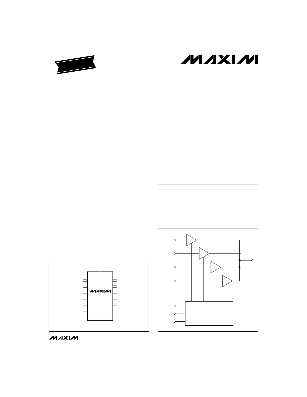
________________Functional Diagram
IN0
AV = +1
MAX4141
__________________Pin Configuration
TOP VIEW
IN0
1
GND
2
IN1
3
GND
IN2
GND
IN3
MAX4141
4
5
6
7
SO
________________________________________________________________
A0
14
A1
13
V
CC
12
OUT
11
V
10
EE
EN
9
N.C.
8
IN1
IN2
IN3
A0
A1
EN
AV = +1
CONTROL
LOGIC
Maxim Integrated Products
Call toll free 1-800-998-8800 for free samples or literature.
AV = +1
OUT
A
= +1
V
1
330MHz, 4x1 Precision Video Multiplexer
ABSOLUTE MAXIMUM RATINGS
VCC...........................................................................................6V
..........................................................................................-6V
V
EE
..................................................................................12V
V
CC-VEE
Analog Input Voltage .......................(V
Digital Input Voltage...................................-0.3V to (V
Duration of Short Circuit to Ground..............Continuous (Note 1)
Note 1: If maximum power-dissipation rating is met.
MAX4141
Stresses beyond those listed under “Absolute Maximum Ratings” may cause permanent damage to the device. These are stress ratings only, and functional
operation of the device at these or any other conditions beyond those indicated in the operational sections of the specifications is not implied. Exposure to
absolute maximum rating conditions for extended periods may affect device reliability.
- 0.3V) to (VCC+ 0.3V)
EE
CC
+ 0.3V)
Continuous Power Dissipation (T
SO (derate 8.00mW/°C above +70°C)........................640mW
Operating Temperature Range...............................0°C to +70°C
Storage Temperature Range.............................-65°C to +160°C
Junction Temperature......................................................+150°C
Lead Temperature (soldering, 10sec).............................+300°C
ELECTRICAL CHARACTERISTICS
(VS= ±5V, -2.5V ≤ VIN≤ +2.5V, RL= 5kΩ, CL= 5pF, TA= 0°C to +70°C, unless otherwise noted. Typical values are at TA= +25°C.)
CONDITIONS
DC PARAMETERS
Operating Supply Voltage
Operating Supply Current
Disabled Supply Current
Input Voltage Range
Input Bias Current
Input Resistance
Input Capacitance
Output Offset Voltage
Voltage Gain
Output Resistance
Disabled Output Current
Disabled Output Resistance
Disabled Output Capacitance
Logic Input High Voltage
Logic Input Low Voltage
Logic Input High Current
Logic Input Low Current
S
I
S(ON)
S(OFF)
IN
I
B
R
IN
IN
V
OS
A
V
OUT
OUT(OFF)
OUT
OUT
INH
INL
INH
INL
Enabled
VIN= 0V
TA= +25°C
TA= T
MIN
to T
Channel selected
Channel disabled
Channel selected
Channel disabled
VIN= 0V, channel enabled or disabled
TA= +25°C
TA= T
MIN
to T
MAX
VS= ±4.5V to ±5.5V
VIN= ±2.5V
V
= 0V
OUT
TA= +25°C
TA= T
MIN
to T
VS= ±4.5V to ±5.5V
= ±4.5V to ±5.5V
V
S
VS= ±4.5V to ±5.5V
VS= ±4.5V to ±5.5V
MAX
MAX
= +70°C)
A
±4.5 ±5.0 ±5.5V
5.0 5.5
6.5
±2.5 ±4.0
±0.2
0.4
100
3
±3 ±10
±15
0.98 1.0
0.97 1.0
UNITSMIN TYP MAXSYMBOLPARAMETER
V
mA
µA250 350I
V±2.5V
µA
MΩ
pFC
mV
dB50PSRRPower-Supply Rejection Ratio
V/V
Ω20R
nA10I
MΩ30R
pF5C
V2.0V
V0.8V
µA10I
µA10I
2 _______________________________________________________________________________________
330MHz, 4x1 Precision Video Multiplexer
ELECTRICAL CHARACTERISTICS (continued)
(VS= ±5V, -2.5V ≤ VIN≤ +2.5V, RL= 5kΩ, CL= 5pF, TA= 0°C to +70°C, unless otherwise noted. Typical values are at TA= +25°C.)
CONDITIONS
AC PARAMETERS
VIN= 5Vp-p
SRSlew Rate
VIN= 1.4Vp-p
Full-Power Bandwidth
(Note 2)
-3dB Bandwidth
Gain Flatness
Small-Signal Rise Time
VIN= 1.4Vp-p
f
PBW
VIN= 5Vp-p
VIN= 0.1Vp-p
3dB
DC to 30MHz
DC to 150MHz
VIN= 0.2Vp-p, 10% to 90%
R
f = 3.58MHz
f = 3.58MHz
VIN= 1Vp-p, f = 30MHz, RIN= 50Ω
VIN= 1Vp-p, f = 30MHz
Channel Switching Off Time
Channel Switching On Time
OFF
ON
f = 3.58MHz
Chip-to-chip, f = 3.58MHz
f = 30MHz, VIN= 1.4Vp-p, RL= 2k
f = 30MHz, VIN= 1.4Vp-p, RL= 2k
Note 2: Full-Power Bandwidth is inferred from Slew Rate (SR) testing by the equation SR = ωE
voltage and ω = 2πf.
Note 3: Differential Gain and Phase are tested using a modulated ramp, 100IRE (0.714V).
700
500
110
45
0.02
±0.1
, where EPis the peak output
P
UNITSMIN TYP MAXSYMBOLPARAMETER
V/µs
MHz
MHz330f
dB
dB0.08Gain Peaking
ps950t
%0.01DGDifferential Gain (Note 3)
degrees0.01DPDifferential Phase (Note 3)
dB66All-Hostile Crosstalk
dB74Off Isolation
µs1.0t
ns500t
mVp-p13Switching Transient
ps860Group Delay
degrees±0.2Input-Output Delay Matching
dBc-65Second Harmonic Distortion
dBc-70Third Harmonic Distortion
MAX4141
MAX4141
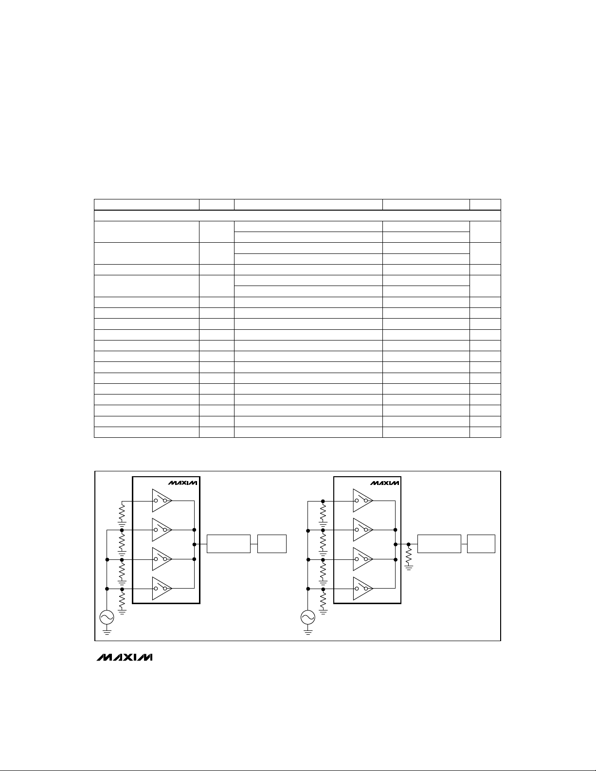
ALL-HOSTILE CROSSTALK TEST CIRCUIT
V
IN
(1Vp-p)
_______________________________________________________________________________________ 3
HIGH-IMPEDANCE
PROBE
NETWORK
ANALYZER
OFF-ISOLATION TEST CIRCUIT
V
IN
(1Vp-p)
MAX4141
HIGH-IMPEDANCE
PROBE
20Ω*
* 20Ω RESISTOR USED TO SIMULATE
OUTPUT RESISTOR OF AN "ON" MAX4141.
IN THIS WAY, OPERATION IN AN ARRAY
IS SIMULATED.
NETWORK
ANALYZER

330MHz, 4x1 Precision Video Multiplexer
__________________________________________Typical Operating Characteristics
(VS= ±5V, RL= 5kΩ, CL= 1pF, TA = +25°C, unless otherwise noted.)
2
0
-2
MAX4141
-4
-6
-8
GAIN (dB)
-10
-12
-14
-16
-18
10
0
-10
-20
-30
-40
-50
AMPLITUDE (dB)
-60
-70
-80
-90
GAIN vs. FREQUENCY
1 10 1000
10k 100k 10M 100M
FREQUENCY (MHz)
POWER-SUPPLY REJECTION RATIO
vs. FREQUENCY
V
FREQUENCY (Hz)
SMALL-SIGNAL PULSE RESPONSE
(CL = 0pF, RL = 5kΩ)
0.3
0.2
MAX4141 TOC-01
0.1
0
-0.1
-0.2
GAIN (dB)
-0.3
-0.4
-0.5
-0.6
100
-0.7
1 10 100
ALL-HOSTILE CROSSTALK
60
40
MAX4141 TOC-04
20
0
-20
EE
V
CC
1M
-40
-60
AMPLITUDE (dB)
-80
-100
-120
-140
0.1 1 100 1000
SMALL-SIGNAL PULSE RESPONSE
GAIN FLATNESS
FREQUENCY (MHz)
vs. FREQUENCY
10
FREQUENCY (MHz)
(CL = 47pF, RL = ∞)
1000
MAX4141 TOC-02
MAX4141 TOC-05
OUTPUT RESISTANCE vs. FREQUENCY
40
30
20
OUTPUT RESISTANCE (Ω)
10
0
0.1 1 100 500
OFF ISOLATION vs. FREQUENCY
60
40
20
0
-20
-40
-60
AMPLITUDE (dB)
-80
-100
-120
-140
0.1 1 100 1000
10
FREQUENCY (MHz)
10
FREQUENCY (MHz)
LARGE-SIGNAL PULSE RESPONSE
(CL = 0pF, RL = 5kΩ)
MAX4141 TOC-03
MAX4141 TOC-06
MAX14141 TOC-09
(2.5V/div)
VOLTS
OUT
(1V/div)
IN
VOLTS
(100mV/div)
TIME (5ns/div)
MAX14141 TOC-07
(100mV/div)
VOLTS
TIME (5ns/div)
4 _______________________________________________________________________________________
TIME (5ns/div)
MAX14141 TOC-08
GND
GND

330MHz, 4x1 Precision Video Multiplexer
____________________________Typical Operating Characteristics (continued)
(TA = +25°C, unless otherwise noted.)
LARGE-SIGNAL PULSE RESPONSE
IN
2.5V/div
VOLTS
OUT
(1V/div)
100
)
30
Hz
10
3
NOISE VOLTAGE (nV √
1
1 100 1M
(CL = 47pF, RL = ∞)
TIME (10ns/div)
NOISE VOLTAGE
vs. FREQUENCY
10k
FREQUENCY (Hz)
350
300
250
200
150
BANDWIDTH (MHz)
100
50
0
0
MAX14141 TOC-10
GND
2V/div
OUTPUT
GND
1V/div
5.0
MAX4141 TOC-13
10G
100M
BANDWIDTH vs.
LOAD CAPACITANCE
20 40 60 80 100
LOAD CAPACITANCE (pF)
4.8
4.6
4.4
4.2
4.0
SUPPLY CURRENT (mA)
3.8
3.6
3.4
070
RL = OPEN
-3dB BW
-0.1dB BW
ENABLE/DISABLE DELAY TIME
10 20 60
MAX4141 TOC-16
ENABLE ON
IN0 ON
TIME (1µs/div)
SUPPLY CURRENT
vs. TEMPERATURE
I
EE
30
40
TEMPERATURE (°C)
GAIN (dB)
I
CC
50
0
-0.2
-0.4
-0.6
-0.8
-1.0
-1.2
-1.4
-1.6
0
OUTPUT GLITCH AMPLITUDE
MAX14141 TOC-11
A0
2V/div
GND
AMPLITUDE
10mV/div
OUTPUT
GAIN vs. INPUT VOLTAGE
-0.085
MAX4141 TOC-14
-0.090
-0.095
GAIN (dB)
-0.100
-0.105
-0.110
-3
-2 -1 0 1 2 3
GAIN vs.
LOAD RESISTANCE
12345
RL(kΩ)
TIME (1µs/div)
AND TEMPERATURE
TA = 0°C
TA = +25°C
TA = +70°C
INPUT VOLTAGE (V)
MAX4141 TOC-17
MAX4141
MAX14141 TOC-12
MAX4141 TOC-15
_______________________________________________________________________________________
5

330MHz, 4x1 Precision Video Multiplexer
______________________________________________________________Pin Description
PIN
Signal InputIN01
GND2, 4, 6
MAX4141
10
12
EN9
EE
CC
Analog (Signal) Ground. Since inputs are isolated by these grounds, they should be as noise-free
as possible.
Signal InputIN13
Signal InputIN25
Signal InputIN37
No Connect—not internally connected.N.C.8
Output Enable and device shutdown. A logic high on this pin enables the output. A logic low
causes the output to assume a high-impedance state and reduces operating current.
Negative Power-Supply Voltage. Decouple to power ground.V
Signal OutputOUT11
Positive Power-Supply Voltage. Decouple to power ground.V
Channel Selection Bit. See truth tables.A113
Channel Selection Bit. See truth tables.A014
_______________Detailed Description
The MAX4141 video switch is manufactured with
Maxim’s proprietary complementary bipolar process
that yields high bandwidth and low capacitance. To
maintain a wide bandwidth, the MAX4141 incorporates
a straightforward structure of input and output buffers.
Make-before-break switching is employed to reduce
noise and glitches, even when switching from part to
part in large arrays. The input buffers provide a constant, high input impedance. And, they prevent the
make-before-break action from feeding back to the
input and causing noise and/or glitches.
The design of the switching mechanism limits the
inevitable glitch to within 13mVp-p. In addition, the
glitch pulse is positive to avoid confusion with any negative sync pulses.
Unity-gain output buffers isolate other inputs from the
switching action of large multiplex arrays. These buffers
can drive 5kΩ resistive loads. Load capacitance is limited only by system bandwidth requirements.
The MAX4141 does not contain buffer latches. The digital inputs control the switch transparently.
DESCRIPTIONFUNCTION
__________Applications Information
Grounding, Bypassing,
and PC Board Layout
In order to obtain the MAX4141’s full 330MHz bandwidth,
Microstrip and Stripline techniques are recommended in
most cases. To ensure your PC board does not degrade
the switch’s performance, it’s wise to design the board
for a frequency greater than 1GHz. Even with very short
runs, it’s good practice to use this technique at critical
points, such as inputs and outputs. Whether you use a
constant-impedance board or not, observe the following
guidelines when designing the board:
• Do not use wire-wrap boards, because they are too
inductive.
• Do not use IC sockets. They increase parasitic
capacitance and inductance.
• In general, surface-mount components have shorter
leads and lower parasitic reactance, and give better
high-frequency performance than through-hole components.
• The PC board should have at least two layers, with
one side a signal layer and the other a ground plane.
• Keep signal lines as short and as straight as possible. Do not make 90° turns; round all corners.
• The ground plane should be as free from voids as
possible.
6 _______________________________________________________________________________________

330MHz, 4x1 Precision Video Multiplexer
On Maxim’s evaluation kit, the ground plane has been
removed from areas where keeping the trace capacitance to a minimum is more important than maintaining
ground continuity. For example, the ground plane has
been removed from beneath the IC to minimize pin
capacitance.
The signal input line is approximately 0.103 inches
wide to minimize inductance and to provide a constant
50Ω impedance path. It is terminated by a 50Ω chip
resistor.
Bypass Components—Capacitors
Electrolytic and tantalum capacitors are available from
0.1µF to over 300µF, but have resonant frequencies
below 1MHz. Ceramic capacitors are highly recommended and are available to 1µF, with the smaller values having resonant frequencies to almost 1GHz. The
less expensive capacitors are constructed using a
multilayer approach; high values are available, but resonant frequencies beyond a few hundred megahertz
are not, because of the inductive effect of the multiple
layers. More expensive, solid dielectric microwave
porcelain/ceramic capacitors are available up to
1000pF with resonant frequencies beyond 20GHz. In all
types, resonant frequency depends on capacitor value,
voltage rating, and physical size; the larger the capacitor, the lower the resonant frequency.
We recommend ceramic surface-mount/chip capacitors. Placement of bypass capacitors on the PC board
is critical, and the smaller chip capacitors allow placement as close to the part as practical. The smaller,
higher frequency capacitors should be placed as close
to the chip as possible, with the higher-value capacitors placed farther away.
The MAX4141 was designed as a building block for
large arrays. The high-power drive required for internal
cable drivers has a negative effect on crosstalk and
increases system power consumption. Figure 1 shows
an 8x1 multiplexer circuit.
Even though the MAX4141 drives capacitive loads, you
may want to limit the number of switches connected
together to maximize bandwidth. The MAX4141 has a
finite input capacitance of about 3pF and a dynamic
output resistance of about 20Ω. This causes a pole at a
little more than 2.6GHz. However, in a large array with
many switch inputs, the total capacitance is (N x 3pF),
where “N” is the number of switches connected in parallel. The pole will be located at:
1
2 N 3pF C 20
π× × +
()
where C
connect.
If the maximum number of switches that may be connected while still maintaining bandwidth is less than
your system requirements, use a unity-gain buffer
amplifier to isolate the switch from the remainder of the
inputs.
is the stray capacitance from the inter-
STRAY
STRAY
×Ω
MHz
Table 1. Truth Table
A1 A0 EN OUT
X X 0 High-Z
0 0 1 IN0
0 1 1 IN1
1 0 1 IN2
1 1 1 IN3
Creating Large Arrays
MAX4141
_______________________________________________________________________________________ 7

330MHz, 4x1 Precision Video Multiplexer
V
10µF
EEVCC
10µF
OUT
(TO CABLE DRIVER OR
OTHER SWITCHES)
MAX4141
75Ω
75Ω
75Ω
75Ω
75Ω
75Ω
75Ω
75Ω
GND
GND
GND
GND
GND
GND
IN0
IN1
IN2
IN3
IN0
IN1
IN2
IN3
1
2
3
4
5
6
7
1
2
3
4
5
6
7
MAX4141
MAX4141
14
13
12
11
10
14
13
12
11
10
8
A0
A1
V
OUT
V
EN
9
N.C.
8
A0
A1
V
OUT
V
EN
9
N.C.
CC
1000pF
EE
1000pF
CC
1000pF
EE
1000pF
EN2
EN1
A1
A0
Figure 1. 8x1 Multiplexer Circuit
Maxim cannot assume responsibility for use of any circuitry other than circuitry entirely embodied in a Maxim product. No circuit patent licenses are
Maxim cannot assume responsibility for use of any circuitry other than circuitry entirely embodied in a Maxim product. No circuit patent licenses are
implied. Maxim reserves the right to change the circuitry and specifications without notice at any time.
implied. Maxim reserves the right to change the circuitry and specifications without notice at any time.
8
___________________Maxim Integrated Products, 120 San Gabriel Drive, Sunnyvale, CA 94086 (408) 737-7600
8
___________________Maxim Integrated Products, 120 San Gabriel Drive, Sunnyvale, CA 94086 (408) 737-7600
© 1995 Maxim Integrated Products Printed USA is a registered trademark of Maxim Integrated Products.
© 1995 Maxim Integrated Products Printed USA is a registered trademark of Maxim Integrated Products.
 Loading...