

_______________General Description
The MAX4130–MAX4134 family of operational amplifiers
combines 10MHz gain-bandwidth product and excellent
DC accuracy with rail-to-rail operation at the inputs and
outputs. These devices require only 900µA per amplifier,
and operate from either a single supply (+2.7V to +6.5V)
or dual supplies (±1.35V to ±3.25V) with a commonmode voltage range that extends 250mV beyond V
EE
and VCC. They are capable of driving 250Ω loads and
are unity-gain stable. In addition, the MAX4131/
MAX4133 feature a shutdown mode in which the outputs
are placed in a high-impedance state and the supply
current is reduced to only 25µA per amplifier.
With their rail-to-rail input common-mode range and
output swing, the MAX4130–MAX4134 are ideal for lowvoltage, single-supply operation. Although the minimum
operating voltage is specified at 2.7V, the devices
typically operate down to 1.8V. In addition, low offset
voltage and high speed make them the ideal signalconditioning stages for precision, low-voltage dataacquisition systems. The MAX4130 comes in the
space-saving SOT23-5 package.
________________________Applications
Battery-Powered Instruments
Portable Equipment
Data-Acquisition Systems
Signal Conditioning
Low-Power, Low-Voltage Applications
____________________________Features
♦ 5-Pin SOT23-5 Package (MAX4130)
♦ +2.7V to +6.5V Single-Supply Operation
♦ Rail-to-Rail Input Common-Mode Voltage Range
♦ Rail-to-Rail Output Voltage Swing
♦ 10MHz Gain-Bandwidth Product
♦ 900µA Quiescent Current per Amplifier
♦ 25µA Shutdown Function (MAX4131/MAX4133)
♦ 200µV Offset Voltage
♦ No Phase Reversal for Overdriven Inputs
♦ Drive 250Ω Loads
♦ Stable with 160pF Capacitive Loads
♦ Unity-Gain Stable
MAX4130–MAX4134
Single/Dual/Quad, Wide-Bandwidth, Low-Power,
Single-Supply, Rail-to-Rail I/O Op Amps
________________________________________________________________
Maxim Integrated Products
1
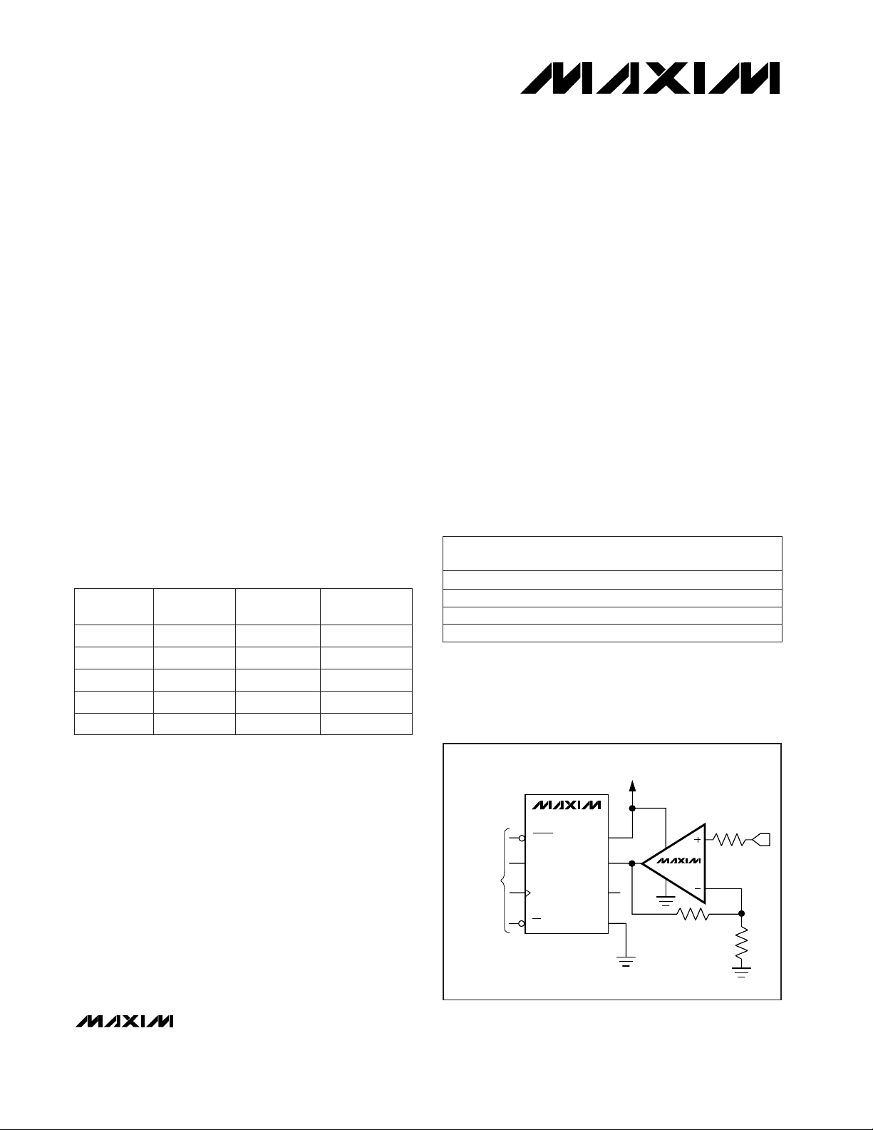
MAX147
MAX4131
SHDN
3
1
2
4
5
6
8
7
V
DD
+3V
AIN
VREF
GND
DOUT
SERIAL
INTERFACE
SCLK
CS
__________Typical Operating Circuit
19-1089; Rev 2; 8/97
______________Ordering Information
AMPS PER
PACKAGE
MAX4130
1
MAX4131
1
PART
MAX4132
2
MAX4133
2
MAX4134
4
SHUTDOWN
MODE
—
Yes
—
Yes
—
PIN-
PACKAGE
5 SOT23-5
8 SO/µMAX
8 SO/µMAX
14 SO
14 SO
PART
MAX4130EUK
MAX4131C/D
MAX4131ESA -40°C to +85°C
0°C to +70°C
-40°C to +85°C
TEMP. RANGE
PIN-
PACKAGE
5 SOT23-5
Dice*
8 SO
SOT
TOP MARK
AABB
—
—
MAX4131EUA -40°C to +85°C 8 µMAX —
____________________Selection Table
Ordering Information continued at end of data sheet.
*Dice are specified at TA= +25°C, DC parameters only.
Pin Configurations appear at end of data sheet.
For free samples & the latest literature: http://www.maxim-ic.com, or phone 1-800-998-8800.
For small orders, phone 408-737-7600 ext. 3468.
MAX4130–MAX4134
Single/Dual/Quad, Wide-Bandwidth, Low-Power,
Single-Supply Rail-to-Rail I/O Op Amps
2 _______________________________________________________________________________________
ABSOLUTE MAXIMUM RATINGS
DC ELECTRICAL CHARACTERISTICS
(VCC= +2.7V to +6.5V, VEE= 0V, VCM= 0V, V
OUT
= VCC/ 2, RLtied to VCC/ 2, SHDN ≥ 2V (or open), TA= +25°C, unless
otherwise noted.)
Stresses beyond those listed under “Absolute Maximum Ratings” may cause permanent damage to the device. These are stress ratings only, and functional
operation of the device at these or any other conditions beyond those indicated in the operational sections of the specifications is not implied. Exposure to
absolute maximum rating conditions for extended periods may affect device reliability.
Supply Voltage (VCC-VEE).....................................................7.5V
IN+, IN-, SHDN Voltage...................(V
CC
+ 0.3V) to (VEE- 0.3V)
Output Short-Circuit Duration (Note 1).......................Continuous
(short to either supply)
Continuous Power Dissipation (T
A
= +70°C)
5-pin SOT23-5 (derate 7.1mW/°C above +70°C) .........571mW
8-pin SO (derate 5.88mW/°C above +70°C).................471mW
8-pin µMAX (derate 4.10mW/°C above +70°C)............330mW
14-pin SO (derate 8.00mW/°C above +70°C)...............640mW
Operating Temperature Range
MAX413_E__ ....................................................-40°C to +85°C
Maximum Junction Temperature .....................................+150°C
Storage Temperature Range.............................-65°C to +160°C
Lead Temperature (soldering, 10sec).............................+300°C
V
CM
= VEEto V
CC
CONDITIONS
nA±1 ±12Input Offset Current
nA±50 ±150Input Bias Current
72 82
Ω0.1Output Resistance
kΩ500Differential Input Resistance
67 90
dB78 100Power-Supply Rejection Ratio
UNITSMIN TYP MAXPARAMETER
V
OUT
= 0.4V to 4.6V, RL= 250Ω 75 86
dBLarge-Signal Voltage Gain
V
VEE- VCC+
0.25 0.25
Common-Mode Input
Voltage Range
Note 1: Provided that the maximum package power-dissipation rating is met.
±0.20 ±0.60
±0.35 ±1.20
±0.35 ±1.50
±0.40 ±1.50
±0.35 ±1.50
Input Offset Voltage
±0.25 ±0.75
VCM= VEEto V
CC
mV
VCM= VEEto V
CC
-1.5V < V
DIFF
< 1.5V
VCC= 2.7V to 6.5V
AV= 1
SHDN < 0.8V, V
OUT
= 0V to V
CC
µA±0.1 ±1Off-Leakage Current
(V
EE
- 0.25V) < VCM<
(VCC+ 0.25V)
78 98
Common-Mode Rejection Ratio
64 84
dB
66 86
74 94
68 88
VCC= 5V
V
OUT
= 0.4V to 2.3V, RL= 250Ω
V
OUT
= 0.25V to 2.45V, RL= 100kΩ
V
OUT
= 0.25V to 4.75V, RL= 100kΩ
VCC= 2.7V
92 108
94 108
MAX4130EUK
MAX4131ESA
MAX4131EUA
MAX4132ESA/MAX4133ESD
MAX4132EUA
MAX4134ESD
MAX4134ESD
MAX4132EUA
MAX4132ESA/MAX4133ESD
MAX4131EUA
MAX4131ESA
MAX4130EUK
MAX4130–MAX4134
Single/Dual/Quad, Wide-Bandwidth, Low-Power,
Single-Supply Rail-to-Rail I/O Op Amps
_______________________________________________________________________________________ 3
DC ELECTRICAL CHARACTERISTICS
(VCC= +2.7V to +6.5V, VEE= 0V, VCM= 0V, V
OUT
= VCC/ 2, RLtied to VCC/ 2, SHDN ≥ 2V (or open), TA= -40°C to +85°C, unless
otherwise noted.)
DC ELECTRICAL CHARACTERISTICS (continued)
(VCC= +2.7V to +6.5V, VEE= 0V, VCM= 0V, V
OUT
= VCC/ 2, RLtied to VCC/ 2, SHDN ≥ 2V (or open), TA= +25°C, unless
otherwise noted.)
RL= 100kΩ
CONDITIONS
20 35
Low
V2.7 6.5Operating Supply-Voltage Range
SHDN > 0.8V, MAX4131–MAX4134
240 290
12 20
VOL- V
EE
125 170
MAX4130/
MAX4131
V
0.8
mA50Output Short-Circuit Current
µA
40 60
Shutdown Supply Current
per Amplifier
UNITS
MIN TYP MAX
PARAMETER
VCC- V
OH
VOL- V
EE
VCC- V
OH
RL= 250Ω
VCC- V
OH
VOL- V
EE
VCC- V
OH
RL= 250Ω
RL= 100kΩ
25 40
mV
280 330
15 30
VOL- V
EE
Output Voltage Swing
180 230
MAX4132/
MAX4133/
MAX4134
High 2.0
SHDN Logic Threshold
MAX4131–MAX4134
VCC= 5V
MAX4131–MAX4134 µA±1 ±3
SHDN Input Current
VCC= 2.7V
VCM= V
OUT
= VCC/ 2 µA
900 1050
VCC= 5V 1000 1150
Supply Current per Amplifier
VCC= 2.7V 25 40
(VEE- 0.2V) < VCM<
(VCC+ 0.2V)
CONDITIONS
±0.75
76
VCM= VEEto V
CC
V
VEE- VCC+
0.20 0.20
Common-Mode Input
Voltage Range
mV
±4.40
±3.50
±4.70
Common-Mode Rejection Ratio
±4.00
Input Offset Voltage
±0.95
VCM= VEEto V
CC
nA±18Input Offset Current
µV/°C±2
60
dB
58
Input Offset Voltage Tempco
MAX4132ESA/MAX4133ESD
60
62
UNITSMIN TYP MAXPARAMETER
VCM= VEEto V
CC
nA±160Input Bias Current
MAX4130EUK
MAX4131ESA
MAX4132ESA/MAX4133ESD
MAX4134ESD
MAX4130EUK
MAX4131ESA
MAX4131EUA
MAX4132EUA
MAX4134ESD
MAX4131EUA
MAX4132EUA
74
MAX4130–MAX4134
Single/Dual/Quad, Wide-Bandwidth, Low-Power,
Single-Supply Rail-to-Rail I/O Op Amps
4 _______________________________________________________________________________________
DC ELECTRICAL CHARACTERISTICS (continued)
(VCC= +2.7V to +6.5V, VEE= 0V, VCM= 0V, V
OUT
= VCC/ 2, RLtied to VCC/ 2, SHDN ≥ 2V (or open), TA= -40°C to +85°C, unless
otherwise noted.)
AC ELECTRICAL CHARACTERISTICS
(VCC= +2.7V to +6.5V, VEE= 0V, SHDN ≥ 2V (or open), TA= +25°C, unless otherwise noted.)
f = 10kHz, V
OUT
= 2Vp-p (AV= 1)
VCC= 0V to 3V step, V
OUT
= V
CC
/ 2 µs
AV= 1, V
OUT
= 2V step
1
pF
Turn-On Time
3Input Capacitance
f = 1kHz
pA/√Hz
f = 1kHz
0.4Input Noise Current Density
%
nV/√Hz
0.003
22Input Noise Voltage Density
CONDITIONS
AV= 1 pF160Capacitive Load Stability
Disable
Enable
MAX4131–MAX4134, VCC= 3V,
V
OUT
= V
CC
/ 2
µs
0.2
SHDN Delay
Total Harmonic Distortion
V/µs4Slew Rate
µs2.0Settling Time to 0.01%
1
MHz10Gain-Bandwidth Product
degrees62Phase Margin
dB12Gain Margin
UNITSMIN TYP MAXPARAMETER
86
Large-Signal Voltage Gain
68
V
OUT
= 0.25V to 4.75V, RL= 100kΩ
V
OUT
= 0.4V to 4.6V, RL= 250Ω
VCC= 5V
84
dB
66
V
OUT
= 0.25V to 2.45V, RL= 100kΩ
V
OUT
= 0.4V to 2.3V, RL= 250Ω
VCC= 2.7V
Off-Leakage Current ±12 µA
SHDN < 0.8V, V
OUT
= 0V to V
CC
MAX4130/
MAX4131
190VOL- V
EE
25
300
MAX4132/
MAX4133/
MAX4134
250
Output Voltage Swing
VOL- V
EE
35
350
mV
50
RL= 100kΩ
RL= 250Ω
VCC- V
OH
VOL- V
EE
VCC- V
OH
40
RL= 100kΩ
RL= 250Ω
VCC- V
OH
VOL- V
EE
VCC- V
OH
PARAMETER
MIN TYP MAX
UNITS
Shutdown Supply Current
per Amplifier
70
µA
Power-Supply Rejection Ratio 74 dB
0.8
V
SHDN < 0.8V, MAX4131–MAX4134
Operating Supply-Voltage Range 2.7 6.5 V
1100
µAVCM= V
OUT
= V
CC
/ 2
VCC= 2.7V
SHDN Input Current
Low
±3
CONDITIONS
µA
50
MAX4131—MAX4134
VCC= 2.7V to 6.5V
VCC= 2.7V
VCC= 5V
MAX4131–MAX4134
Supply Current per Amplifier
SHDN Logic Threshold
1200
2.0High
VCC= 5V
MAX4131–MAX4134
MAX4130–MAX4134
Single/Dual/Quad, Wide-Bandwidth, Low-Power,
Single-Supply, Rail-to-Rail I/O Op Amps
_______________________________________________________________________________________
5
60
-40
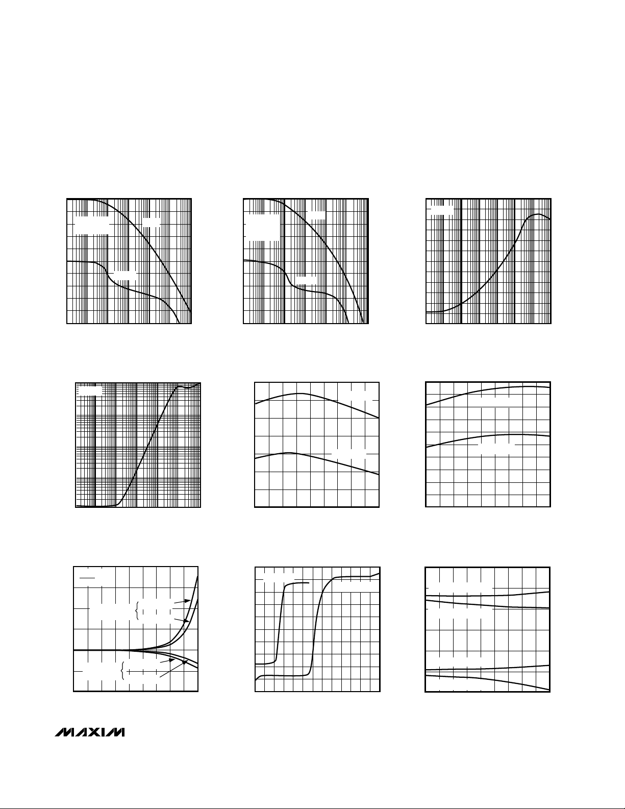
100 1k 10k 1M 10M100k 100M
GAIN AND PHASE
vs. FREQUENCY
-20
FREQUENCY (Hz)
GAIN (dB)
0
20
40
PHASE
GAIN
AV = +1000
NO LOAD
PHASE (DEGREES)
180
144
72
0
-72
-144
-180
-108
-36
36
108
MAX4130/34-01
60
-40
100 1k 10k 1M 10M100k 100M
GAIN AND PHASE
vs. FREQUENCY (WITH C
LOAD
)
-20
MAX4130/34-02
FREQUENCY (Hz)
GAIN (dB)
0
20
40
PHASE
GAIN
AV = +1000
R
L
= ∞
C
L
= 160pF
PHASE (DEGREES)
180
144
72
0
-72
-144
-180
-108
-36
36
108
0
-100
10 100 1k 100k 1M 10M10k 100M
POWER-SUPPLY REJECTION
vs. FREQUENCY
-80
MAX4130/34-03
FREQUENCY (Hz)
PSR (dB)
-60
-40
-20
AV = +1
0
10
5
15
20
25
35
30
45
40
50
-40 -25 -10 5 20 35 50 65 80 95
SHUTDOWN SUPPLY CURRENT
vs. TEMPERATURE
MAX4130/34-07
TEMPERATURE (°C)
SUPPLY CURRENT (µA)
VCC = +6.5V
VCC = +2.7V
100
0.10
0.01
100 1k 100k 1M
10M
10k 100M
OUTPUT IMPEDANCE
vs. FREQUENCY
MAX4130/34-05
FREQUENCY (Hz)
OUTPUT IMPEDANCE (Ω)
1
10
AV = +1
1150
800
850
900
950
1050
1000
1100
-40 -25 -10 5 20 35 50 65 80 95
SUPPLY CURRENT PER AMPLIFIER
vs. TEMPERATURE
MAX4130/34-06
TEMPERATURE (°C)
SUPPLY CURRENT (µA)
VCC = +6.5V
VCC = +2.7V
-10
-5
0
5
10
15
20
-40 -25 -10 5 20 35 50 65 80 95
OUTPUT LEAKAGE CURRENT
vs. TEMPERATURE
MAX4130/34-08
TEMPERATURE (°C)
LEAKAGE CURRENT (µA)
VCC = +6.5V
V
OUT
SHORT
TO V
CC
VCC = +2.7V
VCC = +6.5V
V
OUT
SHORT
TO V
EE
VCC = +2.7V
AV = +1
SHDN = 0V
__________________________________________Typical Operating Characteristics
(VCC= +5V, VEE= 0V, VCM= V
CC
/ 2, TA = +25°C, unless otherwise noted.)
-60
0 1 2 3 4 5 6
INPUT BIAS CURRENT
vs. COMMON-MODE VOLTAGE
MAX4130/34-10
COMMON-MODE VOLTAGE (V)
INPUT BIAS CURRENT (nA)
-50
-40
-30
-20
-10
0
10
20
30
40
VCC = +2.7V
VCC = +6.5V
-60
-40
-40 -25 -10 5 20 35 50 65 80 95
INPUT BIAS CURRENT
vs. TEMPERATURE
MAX4130/34-11
TEMPERATURE (°C)
INPUT BIAS CURRENT (nA)
-20
0
20
40
60
VCC = +6.5V, VCM = V
CC
VCC = +2.7V, VCM = V
EE
VCC = +2.7V, VCM = V
CC
VCC = +6.5V, VCM = V
EE

MAX4130–MAX4134
Single/Dual/Quad, Wide-Bandwidth, Low-Power,
Single-Supply, Rail-to-Rail I/O Op Amps
6 _______________________________________________________________________________________
120
70
75
0 600
110
115
OUTPUT VOLTAGE: EITHER SUPPLY (mV)
GAIN (dB)
300
95
85
90
80
100 200 500
105
100
400
MAX4130/34-19
LARGE-SIGNAL GAIN
vs. OUTPUT VOLTAGE
RL = 500Ω
RL = 100kΩ
RL = 10kΩ
RL = 2kΩ
VCC = +6.5V
R
L
TO V
CC
130
-40 -25 -10 5 20 35 50 65 80 95
LARGE-SIGNAL GAIN
vs. TEMPERATURE
90
120
MAX4130/34-20
TEMPERATURE (°C)
GAIN (dB)
110
100
80
95
125
115
105
VCC = +6.5V, RL TO V
CC
OR V
EE
VCC = +2.7V, RL TO V
CC
OR V
EE
RL = 100kΩ
V
OUT
(p-p) = VCC - 0.6V
1.2
1.3
1.5
1.4
1.6
1.7
1.8
1.9
-40 -25 -10 5 20 35 50 65 80 95
MINIMUM OPERATING VOLTAGE
vs. TEMPERATURE
MAX4130/34-21
TEMPERATURE (°C)
MINIMUM OPERATING VOLTAGE (V)
____________________________ Typical Operating Characteristics (continued)
(VCC= +5V, VEE= 0V, VCM= V
CC
/ 2, TA = +25°C, unless otherwise noted.)
120
80
85
90
95
100
105
110
115
-40 -25 -10 5 20 35 50 65 80 95
COMMON-MODE REJECTION
vs. TEMPERATURE
MAX4130/34-12
TEMPERATURE (°C)
COMMON-MODE REJECTION (dB)
VCM = 0V TO 5.0V
VCM = 0.2V TO 5.2V
VCM = 0.3V TO 5.3V
130
70
0 600
120
OUTPUT VOLTAGE: EITHER SUPPLY (mV)
GAIN (dB)
300
100
90
80
100 200 500
110
400
MAX4130/34-16
LARGE-SIGNAL GAIN
vs. OUTPUT VOLTAGE
VCC = +6.5V
R
L
TO V
EE
RL = 500Ω
RL = 100kΩ
RL = 10kΩ
RL = 2kΩ
120
60
0 600
110
OUTPUT VOLTAGE: EITHER SUPPLY (mV)
GAIN (dB)
300
90
80
70
100 200 500
100
400
MAX4130/34-15
LARGE-SIGNAL GAIN
vs. OUTPUT VOLTAGE
VCC = +2.7V
R
L
TO V
EE
RL = 500Ω
RL = 100kΩ
RL = 10kΩ
RL = 2kΩ
120
80
-40 -25 -10 5 20 35 50 65 80 95
LARGE-SIGNAL GAIN
vs. TEMPERATURE
90
MAX4130/34-17
TEMPERATURE (°C)
GAIN (dB)
105
85
95
115
110
100
VCC = +2.7V,
R
L
TO V
EE
VCC = +6.5V,
R
L
TO V
CC
VCC = +2.7V, RL TO V
CC
V
OUT
(p-p) = V
CC
-1V
R
L
= 500Ω
VCC = +6.5V,
R
L
TO V
EE
120
70
75
0 600
110
115
OUTPUT VOLTAGE: EITHER SUPPLY (mV)
GAIN (dB)
300
95
85
90
80
100 200 500
105
100
400
MAX4130/34-18
LARGE-SIGNAL GAIN
vs. OUTPUT VOLTAGE
RL = 500Ω
RL = 100kΩ
RL = 10kΩ
RL = 2kΩ
VCC = +2.7V
R
L
TO V
CC
-3.00
-2.25
-0.75
-1.50
0
1.50
0.75
2.25
3.00
-40 -25 -10 5 20 35 50 65 80 95
INPUT OFFSET VOLTAGE
vs. TEMPERATURE
MAX4130/34-09
TEMPERATURE (°C)
VOLTAGE (mV)
SOT23-5
PACKAGE
SO PACKAGE

MAX4130–MAX4134
Single/Dual/Quad, Wide-Bandwidth, Low-Power,
Single-Supply, Rail-to-Rail I/O Op Amps
_______________________________________________________________________________________
7
140
80
10k1k 100k 10M1M
CHANNEL SEPARATION
vs. FREQUENCY
MAX4130/34-25a
FREQUENCY (Hz)
CHANNEL SEPARATION (dB)
100
90
130
110
120
VS = +5V
10 100k10k
FREQUENCY (Hz)
100 1k
0.030
0
0.005
0.010
0.015
0.020
0.025
TOTAL HARMONIC DISTORTION
AND NOISE vs. FREQUENCY
MAX4130/34-22A
THD AND NOISE (%)
2Vp-p SIGNAL
500kHz LOWPASS FILTER
R
L
= 10kΩ TO V
CC
/ 2
0.1
0.001
4.0 4.44.2 5.04.84.6
TOTAL HARMONIC DISTORTION AND NOISE
vs. PEAK-TO-PEAK SIGNAL AMPLITUDE
MAX4130/34-23
PEAK-TO-PEAK SIGNAL AMPLITUDE (V)
THD + NOISE (%)
0.01
RL = 100kΩ
RL = 10kΩ
RL = 2kΩ
RL = 250Ω
AV = +1
10kHz SINE WAVE
R
L
TO V
CC
/ 2
500kHz LOWPASS FILTER
IN
TIME (200ns/div)
VOLTAGE (50mV/div)
OUT
MAX4131
SMALL-SIGNAL TRANSIENT
RESPONSE (NONINVERTING)
MAX4130/34-24
AV = +1
IN
TIME (200ns/div)
VOLTAGE (50mV/div)
OUT
MAX4131
SMALL-SIGNAL TRANSIENT
RESPONSE (INVERTING)
MAX4130/34-25
AV = -1
IN
TIME (2µs/div)
VOLTAGE (2V/div)
OUT
MAX4131
LARGE-SIGNAL TRANSIENT
RESPONSE (NONINVERTING)
MAX4130/34-26
AV = +1
IN
TIME (2µs/div)
VOLTAGE (2V/div)
OUT
MAX4131
LARGE-SIGNAL TRANSIENT
RESPONSE (INVERTING)
MAX4130/34-27
AV = -1
____________________________Typical Operating Characteristics (continued)
(VCC= +5V, VEE= 0V, VCM= V
CC
/ 2, TA = +25°C, unless otherwise noted.)
160
0
-40 -25 -10 5 20 35 50 65 80 95
MINIMUM OUTPUT VOLTAGE
vs. TEMPERATURE
20
140
120
MAX4130/34-13
TEMPERATURE (°C)
V
OUT
- V
EE
(mV)
100
80
60
40
RL TO V
CC
VCC = +6.5V, RL = 500Ω
VCC = +2.7V, RL = 100kΩ
VCC = +2.7V, RL = 500Ω
VCC = +6.5V, RL = 100kΩ
0
50
100
150
200
250
300
-40 -25 -10 5 20 35 50 65 80 95
MAXIMUM OUTPUT VOLTAGE
vs. TEMPERATURE
MAX4130/34-14
TEMPERATURE (°C)
V
CC
- V
OUT
(mV)
RL TO V
EE
VCC = +6.5V, RL = 500Ω
VCC = +2.7V, RL = 100kΩ (BOTTOM)
VCC = +2.7V, RL = 500Ω
VCC = +6.5V, RL = 100kΩ (TOP)

MAX4130–MAX4134
Single/Dual/Quad, Wide-Bandwidth, Low-Power,
Single-Supply, Rail-to-Rail I/O Op Amps
8 _______________________________________________________________________________________
______________________________________________________________Pin Description
Inverting Inputs for amps 1 and 2IN1-, IN2-—
Noninverting Inputs for amps 1 and 2IN1+, IN2+—
Shutdown Control, independent for amps 1
and 2. Tie high or leave floating to enable
amplifier.
SHDN1,
SHDN2
—
Outputs for amps 3 and 4
OUT3,
OUT4
—
Inverting Inputs for amps 3 and 4IN3-, IN4-—
Positive SupplyV
CC
5
No Connect. Not internally connected.N.C.—
Shutdown Control. Tie high or leave floating
to enable amplifier.
SHDN
—
Outputs for amps 1 and 2
OUT1,
OUT2
—
Inverting InputIN-4
Noninverting Input IN+3
MAX4130
Negative Supply. Ground for single-supply
operation.
V
EE
2
OutputOUT1
FUNCTIONNAME
—
—
—
—
—
7
1, 5
8
—
2
3
MAX4131
4
6
2, 6
3, 5
—
—
—
8
—
—
1, 7
—
—
MAX4132
4
—
2, 12
3, 11
6, 9
—
—
14
5, 7, 8, 10
—
1, 13
—
—
MAX4133
4
—
2, 6
3, 5
—
8, 14
9, 13
4
—
—
1, 7
—
—
MAX4134
11
—
Noninverting Inputs for amps 3 and 4IN3+, IN4+— — — — 10, 12
Figure 1a. Reducing Offset Error Due to Bias Current
(Noninverting)
R3
R3 = R1 R2
R1 R2
MAX4130
MAX4131
MAX4132
MAX4133
MAX4134
Figure 1b. Reducing Offset Error Due to Bias Current
(Inverting)
MAX4130
MAX4131
MAX4132
MAX4133
R3
R3 = R1 R2
R1 R2
MAX4134

MAX4130–MAX4134
Single/Dual/Quad, Wide-Bandwidth, Low-Power,
Single-Supply, Rail-to-Rail I/O Op Amps
_______________________________________________________________________________________ 9
__________Applications Information
Rail-to-Rail Input Stage
Devices in the MAX4130–MAX4134 family of highspeed amplifiers have rail-to-rail input and output
stages designed for low-voltage, single-supply operation. The input stage consists of separate NPN and
PNP differential stages that combine to provide an
input common-mode range that extends 0.2V beyond
the supply rails. The PNP stage is active for input voltages close to the negative rail, and the NPN stage is
active for input voltages near the positive rail. The input
offset voltage is typically below 200µV. The switchover
transition region, which occurs near V
CC
/ 2, has been
extended to minimize the slight degradation in common-mode rejection ratio caused by the mismatch of
the input pairs. Their low offset voltage, high bandwidth, and rail-to-rail common-mode range make these
op amps excellent choices for precision, low-voltage
data-acquisition systems.
Since the input stage switches between the NPN and
PNP pairs, the input bias current changes polarity as
the input voltage passes through the transition region.
Reduce the offset error caused by input bias currents
flowing through external source impedances by matching the effective impedance seen by each input
(Figures 1a, 1b). High source impedances, together
with input capacitance, can create a parasitic pole that
produces an underdamped signal response. Reducing
the input impedance or placing a small (2pF to 10pF)
capacitor across the feedback resistor improves
response.
The MAX4130–MAX4134’s inputs are protected from
large differential input voltages by 1kΩ series resistors
and back-to-back triple diodes across the inputs
(Figure 2). For differential input voltages less than 1.8V,
input resistance is typically 500kΩ. For differential input
voltages greater than 1.8V, input resistance is approximately 2kΩ. The input bias current is given by the following equation:
I =
V - 1.8V
2k
BIAS
DIFF
Ω
1k
1k
Figure 2. Input Protection Circuit

MAX4130–MAX4134
Single/Dual/Quad, Wide-Bandwidth, Low-Power,
Single-Supply, Rail-to-Rail I/O Op Amps
10 ______________________________________________________________________________________
Rail-to-Rail Output Stage
The minimum output voltage is within millivolts of
ground for single-supply operation where the load is
referenced to ground (VEE). Figure 3 shows the input
voltage range and output voltage swing of a MAX4131
connected as a voltage follower. With a +3V supply
and the load tied to ground, the output swings from
0.00V to 2.90V. The maximum output voltage swing
depends on the load, but will be within 150mV of a +3V
supply, even with the maximum load (500Ω to ground).
Driving a capacitive load can cause instability in most
high-speed op amps, especially those with low quiescent current. The MAX4130–MAX4134 have a high tolerance for capacitive loads. They are stable with
capacitive loads up to 160pF. Figure 4 gives the stable
operating region for capacitive loads. Figures 5 and 6
show the response with capacitive loads and the
results of adding an isolation resistor in series with the
output (Figure 7). The resistor improves the circuit’s
phase margin by isolating the load capacitor from the
op amp’s output.
IN
TIME (1µs/div)
VOLTAGE (1V/div)
OUT
VCC = 3V, RL = 10kΩ to V
EE
Figure 3. Rail-to-Rail Input/Output Voltage Range
500
0
50
100
150
200
300
350
400
450
0.1 1 10010
LOAD RESISTANCE (kΩ)
LOAD CAPACITANCE (pF)
250
UNSTABLE
OPERATING
REGION
STABLE
OPERATING
REGION
RL to V
EE
V
OUT
= VCC/2
Figure 4. Capacitive-Load Stability
IN
TIME (200ns/div)
VOLTAGE (50mV/div)
OUT
VCC = 5V
R
L
= 10kΩ
C
L
= 130pF
Figure 5. MAX4131 Small-Signal Transient Response with
Capacitive Load
Figure 6. MAX4131 Transient Response to Capacitive Load
with Isolation Resistor
IN
TIME (500ns/div)
VOLTAGE (50mV/div)
OUT
VCC = 5V
C
L
= 1000pF
R
S
= 39Ω

MAX4130–MAX4134
Single/Dual/Quad, Wide-Bandwidth, Low-Power,
Single-Supply, Rail-to-Rail I/O Op Amps
______________________________________________________________________________________ 11
Power-Up and Shutdown Mode
The MAX4130–MAX4134 amplifiers typically settle within 1µs after power-up. Figures 9 and 10 show the output voltage and supply current on power-up, using the
test circuit of Figure 8.
The MAX4131 and MAX4133 have a shutdown option.
When the shutdown pin (SHDN) is pulled low, the supply current drops below 25µA per amplifier and the
amplifiers are disabled with the outputs in a highimpedance state. Pulling SHDN high or leaving it floating enables the amplifier. In the dual-amplifier
MAX4133, the shutdown functions operate independently. Figures 11 and 12 show the output voltage and
supply current responses of the MAX4131 to a shutdown pulse, using the test circuit of Figure 8.
R
S
C
L
Figure 7. Capacitive-Load Driving Circuit
SHDN
OUT
0V TO 2.7V
STEP FOR
SHUTDOWN
TEST
0V TO 2.7V STEP
FOR POWER-UP
TEST; 2.7V FOR
SHUTDOWN
ENABLE TEST.
SUPPLY-CURRENT
MONITORING POINT
V
CC
*0.1µF
10Ω
2k
*FOR SHUTDOWN TEST ONLY.
10k
2k
Figure 8. Power-Up/Shutdown Test Circuit
V
CC
TIME (5µs/div)
VOLTAGE (1V/div)
OUT
Figure 9. Power-Up Output Voltage
V
CC
(1V/div)
TIME (5µs/div)
I
EE
(500µA/div)
Figure 10. Power-Up Supply Current

MAX4130–MAX4134
Single/Dual/Quad, Wide-Bandwidth, Low-Power,
Single-Supply, Rail-to-Rail I/O Op Amps
12 ______________________________________________________________________________________
Power Supplies and Layout
The MAX4130–MAX4134 operate from a single +2.7V
to +6.5V power supply, or from dual supplies of ±1.35V
to ±3.25V. For single-supply operation, bypass the
power supply with a 0.1µF ceramic capacitor in parallel
with at least 1µF. For dual supplies, bypass each supply to ground.
Good layout improves performance by decreasing the
amount of stray capacitance at the op amp’s inputs
and outputs. Decrease stray capacitance by placing
external components close to the op amp’s pins, minimizing trace lengths and resistor leads.
SHDN
TIME (1µs/div)
VOLTAGE (1V/div)
OUT
Figure 11. Shutdown Output Voltage
SHDN
1V/div
TIME (1µs/div)
SUPPLY
CURRENT
500µA/div
Figure 12. Shutdown Enable/Disable Supply Current

MAX4130–MAX4134
Single/Dual/Quad, Wide-Bandwidth, Low-Power,
Single-Supply, Rail-to-Rail I/O Op Amps
______________________________________________________________________________________ 13
__________________________________________________________Pin Configurations
V
EE
IN-
IN+
1
5
V
CC
OUT
MAX4130
SOT23-5
TOP VIEW
2
3
4
14
13
12
11
10
9
8
1
2
3
4
5
6
7
V
CC
OUT2
IN2-
IN2+
V
EE
IN1+
IN1-
OUT1
MAX4133
N.C.
SHDN2
N.C.
N.C.
SHDN1
N.C.
SO
14
13
12
11
10
9
8
1
2
3
4
5
6
7
OUT4
IN4IN4+
V
EE
V
CC
IN1+
IN1-
OUT1
MAX4134
IN3+
IN3OUT3
OUT2
IN2-
IN2+
SO
IN2-
IN1+
IN2+
V
EE
1
2
8
7
V
CC
OUT2
IN1-
OUT1
MAX4132
SO/µMAX
3
4
6
5
OUT
IN1+
N.C.
V
EE
1
2
8
7
SHDN
V
CC
IN1-
N.C.
MAX4131
SO/µMAX
3
4
6
5

MAX4130–MAX4134
Single/Dual/Quad, Wide-Bandwidth, Low-Power,
Single-Supply, Rail-to-Rail I/O Op Amps
14 ______________________________________________________________________________________
__________________________________________________________Chip Topographies
___________________Chip Information_Ordering Information (continued)
SHDN
V
CC
0.055"
(1.397mm)
0.036"
(0.914mm)
OUT
V
EE
IN-
iN+
V
EE
TRANSISTOR COUNT: 170
SUBSTRATE CONNECTED TO V
EE
OUT2
IN2-
IN2+
0.066"
(1.676mm)
0.053"
(1.346mm)
VCCSHDN1
SHDN2
VEEV
CC
OUT1
V
CC
IN1-
IN1+
V
EE
TRANSISTOR COUNT: 340
SUBSTRATE CONNECTED TO V
EE
MAX4131 MAX4133
MAX4130 TRANSISTOR COUNT: 170
MAX4132 TRANSISTOR COUNT: 340
MAX4134 TRANSISTOR COUNT: 680
PART
MAX4132ESA
MAX4132EUA
MAX4133C/D
0°C to +70°C
-40°C to +85°C
-40°C to +85°C
TEMP. RANGE
PIN-
PACKAGE
8 SO
8 µMAX
Dice*
SOT
TOP MARK
—
—
—
MAX4133ESD -40°C to +85°C 14 SO —
*
Dice are specified at TA= +25°C, DC parameters only.
MAX4134ESD
-40°C to +85°C 14 SO —

MAX4130–MAX4134
Single/Dual/Quad, Wide-Bandwidth, Low-Power,
Single-Supply, Rail-to-Rail I/O Op Amps
______________________________________________________________________________________ 15
________________________________________________________Package Information
L
DIM
A
A1
A2
b
C
D
E
E1
L
e
e1
α
MIN
0.90
0.00
0.90
0.35
0.08
2.80
2.60
1.50
0.35
0°
MAX
1.45
0.15
1.30
0.50
0.20
3.00
3.00
1.75
0.55
10°
MILLIMETERS
α
5-PIN SOT23-5
SMALL-OUTLINE
TRANSISTOR PACKAGE
D
e1
A
A2
A1
C
b
e
E1
21-0057B
E
0.95ref
1.90ref
L
α
C
A1B
DIM
A
A1
B
C
D
E
e
H
L
α
MIN
0.036
0.004
0.010
0.005
0.116
0.116
0.188
0.016
0°
MAX
0.044
0.008
0.014
0.007
0.120
0.120
0.198
0.026
6°
MIN
0.91
0.10
0.25
0.13
2.95
2.95
4.78
0.41
0°
MAX
1.11
0.20
0.36
0.18
3.05
3.05
5.03
0.66
6°
INCHES MILLIMETERS
8-PIN µMAX
MICROMAX SMALL-OUTLINE
PACKAGE
0.650.0256
A
e
E H
D
0.101mm
0.004 in
21-0036D

MAX4130–MAX4134
Single/Dual/Quad, Wide-Bandwidth, Low-Power,
Single-Supply, Rail-to-Rail I/O Op Amps
___________________________________________Package Information (continued)
DIM
A
A1
B
C
E
e
H
L
MIN
0.053
0.004
0.014
0.007
0.150
0.228
0.016
MAX
0.069
0.010
0.019
0.010
0.157
0.244
0.050
MIN
1.35
0.10
0.35
0.19
3.80
5.80
0.40
MAX
1.75
0.25
0.49
0.25
4.00
6.20
1.27
INCHES MILLIMETERS
21-0041A
Narrow SO
SMALL-OUTLINE
PACKAGE
(0.150 in.)
DIM
D
D
D
MIN
0.189
0.337
0.386
MAX
0.197
0.344
0.394
MIN
4.80
8.55
9.80
MAX
5.00
8.75
10.00
INCHES MILLIMETERS
PINS
8
14
16
1.270.050
L
0°-8°
HE
D
e
A
A1
C
0.101mm
0.004in.
B
Maxim cannot assume responsibility for use of any circuitry other than circuitry entirely embodied in a Maxim product. No circuit patent licenses are
implied. Maxim reserves the right to change the circuitry and specifications without notice at any time.
16
____________________Maxim Integrated Products, 120 San Gabriel Drive, Sunnyvale, CA 94086 408-737-7600
© 1997 Maxim Integrated Products Printed USA is a registered trademark of Maxim Integrated Products.
 Loading...