Maxim MAX4309ESA, MAX4308ESA, MAX4109ESA, MAX4108ESA Datasheet

For free samples & the latest literature: http://www.maxim-ic.com, or phone 1-800-998-8800
_______________General Description
The MAX4108/MAX4109/MAX4308/MAX4309 op amps
combine ultra-high-speed performance with ultra-lowdistortion operation. The MAX4108 is compensated for
unity-gain stability; the MAX4109, MAX4308, and
MAX4309 are compensated for minimum closed-loop
gains (A
VCL
) of 2V/V, 5V/V, and 10V/V, respectively.
The MAX4108 delivers a 400MHz unity-gain bandwidth
with a 1200V/µs slew rate. An ultra-low-distortion design
provides an unprecedented spurious-free dynamic
range of -93dBc (MAX4108) at 5MHz (V
OUT
= 2Vp-p, R
L
= 100Ω), making these amplifiers ideal for high-performance RF signal processing.
These high-speed op amps feature a wide output voltage swing and a high-current output-drive capability of
90mA.
________________________Applications
High-Speed ADC/DAC Preamp
RGB and Composite Video
High-Performance Receivers
Pulse/RF Amplifier
Active Filters
Ultrasound
Broadcast and High-Definition TV
____________________________Features
♦ High Speed:
400MHz Unity-Gain Bandwidth (MAX4108)
225MHz -3dB Bandwidth (A
VCL
= +2, MAX4109)
220MHz -3dB Bandwidth (A
VCL
= +5, MAX4308)
200MHz -3dB Bandwidth (A
VCL
= +10, MAX4309)
♦ 1200V/µs Slew Rate
♦ Excellent Spurious-Free Dynamic Range:
-93dBc at fC= 5MHz (MAX4108)
-90dBc at fC= 5MHz (MAX4109)
♦ 100MHz 0.1dB Gain Flatness (MAX4108)
♦ High Full-Power Bandwidth: 300MHz
(MAX4108, VO= 2Vp-p)
♦ High Output Drive: 90mA
♦ Output Short-Circuit Protected
♦ Low Differential Gain/Phase: 0.004%/0.008°
MAX4108/MAX4109/MAX4308/MAX4309
400MHz, Ultra-Low-Distortion Op Amps
________________________________________________________________
Maxim Integrated Products
1
19-0461; Rev 2; 4/97
PART
MAX4108ESA
MAX4109ESA
-40°C to +85°C
-40°C to +85°C
TEMP. RANGE PIN-PACKAGE
8 SO
8 SO
______________Ordering Information
OUT
IN+
V
EE
V
EE
1
2
8
7
V
CC
V
CC
IN-
N.C.
MAX4108
MAX4109
MAX4308
MAX4309
SO
TOP VIEW
3
4
6
5
__________________Pin Configuration
300Ω
300Ω
300Ω
300Ω
53.6Ω*
60Ω*
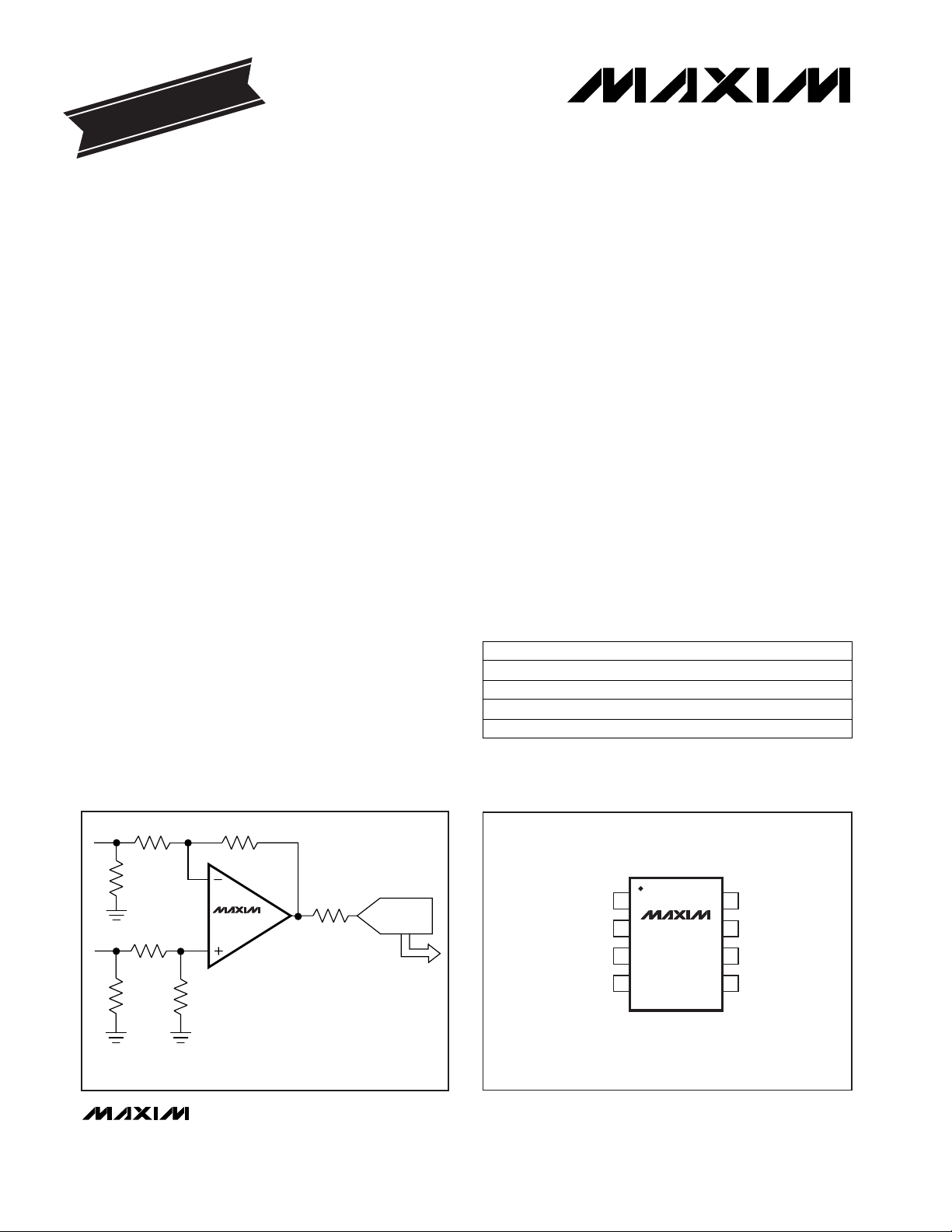
DIFFERENCE AMPLIFIER/ADC PREAMPLIFIER
10Ω
MAX4109
12-BIT ADC
* USED TO MATCH A 50Ω
SOURCE IMPEDANCE
________Typical Application Circuit
EVALUATION KIT
AVAILABLE
MAX4308ESA
MAX4309ESA
-40°C to +85°C
-40°C to +85°C 8 SO
8 SO

MAX4108/MAX4109/MAX4308/MAX4309
400MHz, Ultra-Low-Distortion Op Amps
2 _______________________________________________________________________________________
ABSOLUTE MAXIMUM RATINGS
ELECTRICAL CHARACTERISTICS
(VCC= +5V, VEE= -5V, TA= T
MIN
to T
MAX
, typical values are at TA= +25°C, unless otherwise noted.)
Stresses beyond those listed under “Absolute Maximum Ratings” may cause permanent damage to the device. These are stress ratings only, and functional
operation of the device at these or any other conditions beyond those indicated in the operational sections of the specifications is not implied. Exposure to
absolute maximum rating conditions for extended periods may affect device reliability.
Supply Voltage (VCCto VEE)..................................................12V
Voltage on Any Pin to Ground or
Any Other Pin..............................(V
EE
- 0.3V) to (VCC+ 0.3V)
Short-Circuit Duration (OUT to GND).........................Continuous
Continuous Power Dissipation (T
A
= +70°C)
SO (derate 5.88mW/°C above +70°C)........................471mW
Operating Temperature Range ...........................-40°C to +85°C
Storage Temperature Range.............................-65°C to +150°C
Junction Temperature......................................................+150°C
Lead Temperature (soldering, 10sec).............................+300°C
V
OUT
= 0V
Short to ground
V
OUT
= 0V
RL= 33Ω, TA= 0°C to +85°C
VIN= 0V
V
OUT
= 0V, VIN= -V
OS
V
OUT
= 0V, VIN= -V
OS
Either input
VCM= ±2.5V
Either input
f = 10kHz
CONDITIONS
mA100I
SC
Short-Circuit Output Current
mA65 90I
OUT
Output Current Drive
mA20 27I
S
Quiescent Supply Current
dB70 100CMRCommon-Mode Rejection
pA/√Hz2i
n
Input Current Noise
µV/°C13TCV
OS
Input Offset Voltage Drift
mV1 8V
OS
Input Offset Voltage
6
µA12 34I
B
Input Bias Current
µA0.05 2.5I
OS
Input Offset Current
MΩ1.5R
INCM
Common-Mode Input
Resistance
pF1C
INCM
Common-Mode Input
Capacitance
UNITSMIN TYP MAXSYMBOLPARAMETER
VS= ±4.5V to ±5.5V dB70 90PSRPower-Supply Rejection
RL= 100Ω
RL= ∞
V
2.5 to 2.7 to
-3.1 -3.7
V
OUT
Output Voltage Swing
2.5 to 2.9 to
-3.1 -3.8
V
OUT
= ±2.0V, VCM= 0V, RL= 100Ω dBA
OL
Open-Loop Voltage Gain 70 100
V-2.5 2.5V
CM
Common-Mode Input Voltage
µV
RMS
75
fB= 1MHz to 100MHz nA
RMS
25I
n
Integrated Current Noise
nV/√Hzf = 10kHze
n
Input Voltage Noise
fB= 1MHz to 100MHzE
nRMS
Integrated Voltage Noise
225MAX4109
MHz
220
200
MAX4308
BW
-3dB
-3dB Bandwidth V
OUT
≤ 0.1V
RMS
MAX4309
400MAX4108
DC SPECIFICATIONS (RL= ∞)
AC SPECIFICATIONS (RL= 100Ω)

MAX4108/MAX4109/MAX4308/MAX4309
400MHz, Ultra-Low-Distortion Op Amps
_______________________________________________________________________________________ 3
ELECTRICAL CHARACTERISTICS (continued)
(VCC= +5V, VEE= -5V, TA= T
MIN
to T
MAX
, typical values are at TA= +25°C, unless otherwise noted.)
-50mV ≤ V
OUT
≤ 50mV
-2V ≤ V
OUT
≤ 2V
To 0.01%
To 0.1%
MAX4109, A
VCL
= +2
MAX4108, A
VCL
= +1
MAX4309
MAX4308
MAX4108
MAX4309, A
VCL
= +10
MAX4109
MAX4308, A
VCL
= +5
CONDITIONS
%0.004DGDifferential Gain
nsRise/Fall Times
2
f = 3.58MHz, RL= 150Ω degrees
3
tR, t
F
0.008
ns
12
t
S
Settling Time
DP
8
Differential Phase
V/µs1200
pF2C
IN
Input Capacitance
f = 10MHz Ω1R
OUT
MHz
30
BW
0.1dB
0.1dB Gain Flatness
Output Resistance
100
25
100
MHz
130
FPBWFull-Power Bandwidth
190
300
200
UNITSMIN TYP MAXSYMBOLPARAMETER
f = 3.58MHz, RL= 150Ω
10% to 90%
-1V ≤ V
OUT
≤ 1V
-2V ≤ V
OUT
≤ 2V
V
OUT
= 2Vp-p
SRSlew Rate
fC= 20MHz,
RL= 100Ω
fC= 5MHz,
RL= 100Ω
-81
-93
MAX4108,
V
OUT
= 2Vp-p, A
VCL
= +1
fC= 20MHz,
RL= 100Ω
fC= 5MHz,
RL= 100Ω
-80
-90
MAX4109,
V
OUT
= 2Vp-p, A
VCL
= +2
fC= 20MHz,
RL= 100Ω
fC= 5MHz,
R
L
= 100Ω
fC= 20MHz,
RL= 100Ω
fC= 5MHz,
RL= 100Ω
dBcSpurious-Free Dynamic Range
-80
-80
-83
-83
SFDR
MAX4309,
V
OUT
= 2Vp-p, A
VCL
= +10
MAX4308,
V
OUT
= 2Vp-p, A
VCL
= +5
MAX4308
MAX4108
dBmThird-Order Intercept
46
39
IP3 fC= 10MHz
36
43
MAX4109
MAX4309
AC SPECIFICATIONS (RL= 100Ω) (continued)

MAX4108/MAX4109/MAX4308/MAX4309
400MHz, Ultra-Low-Distortion Op Amps
4 _______________________________________________________________________________________
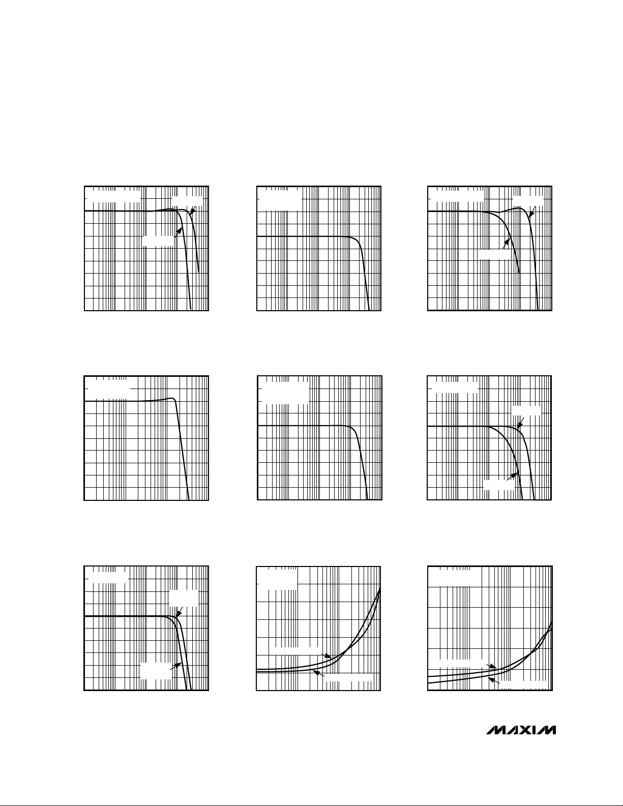
__________________________________________Typical Operating Characteristics
(VCC= +5V, VEE= -5V, RL= 100Ω, TA= +25°C, unless otherwise noted.)
2
1
-8
0.1 1 10 100 1000
MAX4108
SMALL-SIGNAL GAIN vs. FREQUENCY
-6
-7
MAX4108/9-A
FREQUENCY (MHz)
NORMALIZED GAIN (dB)
-4
-5
-2
-3
0
-1
V
OUT
≤ 100mVp-p
A
VCL
= +1
A
VCL
= +2
2
1
0
-8
0.1 1 100 1000
MAX4109
SMALL-SIGNAL GAIN vs. FREQUENCY
-4
-5
-6
-7
-1
-2
-3
MAX4108/9-C
FREQUENCY (MHz)
NORMALIZED GAIN (dB)
10
A
VCL
= +5
A
VCL
= +2
V
OUT
≤ 100mVp-p
2
1
0
-8
1 100 1000
MAX4109
LARGE-SIGNAL GAIN vs. FREQUENCY
-4
-5
-6
-7
-1
-2
-3
MAX4108/9-D
FREQUENCY (MHz)
NORMALIZED GAIN (dB)
10
V
OUT
= 2Vp-p
A
VCL
= +2
4
-6
0.1 10 1001 1000
MAX4309
SMALL-SIGNAL GAIN vs. FREQUENCY
-4
-5
MAX4308/9 TOCF
FREQUENCY (MHz)
NORMALIZED GAIN (dB)
-2
-3
0
-1
2
1
3
V
OUT
≤ 100mVp-p
A
VCL
= +20
A
VCL
= +10
4
3
-6
0.1 1 10 100 1000
MAX4108
LARGE-SIGNAL GAIN vs. FREQUENCY
-4
-5
MAX4108/9-B
FREQUENCY (MHz)
GAIN (dB)
-2
-3
0
-1
2
1
V
OUT
= 2Vp-p
A
VCL
= +1
4
-6
0.1 10 1001 1000
MAX4308
SMALL-SIGNAL GAIN vs. FREQUENCY
-4
-5
MAX4308/9 TOCE
FREQUENCY (MHz)
NORMALIZED GAIN (dB)
-2
-3
0
-1
2
1
3
V
OUT
≤ 100mVp-p
A
VCL
= +5
4
-6
0.1 10 1001 1000
MAX4308/MAX4309
LARGE-SIGNAL GAIN vs. FREQUENCY
-4
-5
MAX4308/9 TOCG
FREQUENCY (MHz)
NORMALIZED GAIN (dB)
-2
-3
0
-1
2
1
3
V
OUT
= 2Vp-p
MAX4309
A
VCL
= +10
MAX4308
A
VCL
= +5
-50
-40
-110
0.1 100
-80
-100
-90
-60
-70
MAX4108/9-H
FREQUENCY (MHz)
HARMONIC DISTORTION (dBc)
1 10
MAX4108
HARMONIC DISTORTION vs. FREQUENCY
2ND HARMONIC
3RD HARMONIC
V
OUT
= 2Vp-p
A
VCL
= +1
10
-110
0.1 100
-50
-90
-70
-10
-30
MAX4108/9-i
FREQUENCY (MHz)
HARMONIC DISTORTION (dBc)
1 10
2ND HARMONIC
V
OUT
= 2Vp-p
A
VCL
= +2
MAX4109
HARMONIC DISTORTION vs. FREQUENCY
3RD HARMONIC
 Loading...