

Page 1
For free samples & the latest literature: http://www.maxim-ic.com, or phone 1-800-998-8800.
For small orders, phone 1-800-835-8769.
General Description
The MAX4104/MAX4105/MAX4304/MAX4305 op amps
feature ultra-high speed, low noise, and low distortion in
a SOT23 package. The unity-gain-stable MAX4104
requires only 20mA of supply current while delivering
625MHz bandwidth and 400V/µs slew rate. The
MAX4304, compensated for gains of +2V/V or greater,
delivers a 730MHz bandwidth and a 1000V/µs slew
rate. The MAX4105 is compensated for a minimum gain
of +5V/V and delivers a 410MHz bandwidth and a
1400V/sec slew rate. The MAX4305 has +10V/V minimum gain compensation and delivers a 340MHz bandwidth and a 1400V/µs slew rate.
Low voltage noise density of 2.1nV/√Hz and -88dBc
spurious-free dynamic range make these devices ideal
for low-noise/low-distortion video and telecommunications applications. These op amps also feature a wide
output voltage swing of ±3.7V and ±70mA output currentdrive capability. For space-critical applications, they
are available in a miniature 5-pin SOT23 package.
________________________Applications
Video ADC Preamp
Pulse/RF Telecom Applications
Video Buffers and Cable Drivers
Ultrasound
Active Filters
ADC Input Buffers
Features
♦ Low 2.1nV/√Hz Voltage Noise Density
♦ Ultra-High 740MHz -3dB Bandwidth (MAX4304,
A
VCL
= 2V/V)
♦ 100MHz 0.1dB Gain Flatness (MAX4104/4105)
♦ 1400V/µs Slew Rate (MAX4105/4305)
♦ -88dBc SFDR (5MHz, R
L
= 100Ω) (MAX4104/4304)
♦ High Output Current Drive: ±70mA
♦ Low Differential Gain/Phase Error: 0.01%/0.01°
(MAX4104/4304)
♦ Low ±1mV Input Offset Voltage
♦ Available in Space-Saving 5-Pin SOT23 Package
MAX4104/MAX4105/MAX4304/MAX4305
740MHz, Low-Noise, Low-Distortion
Op Amps in SOT23-5
________________________________________________________________
Maxim Integrated Products
1
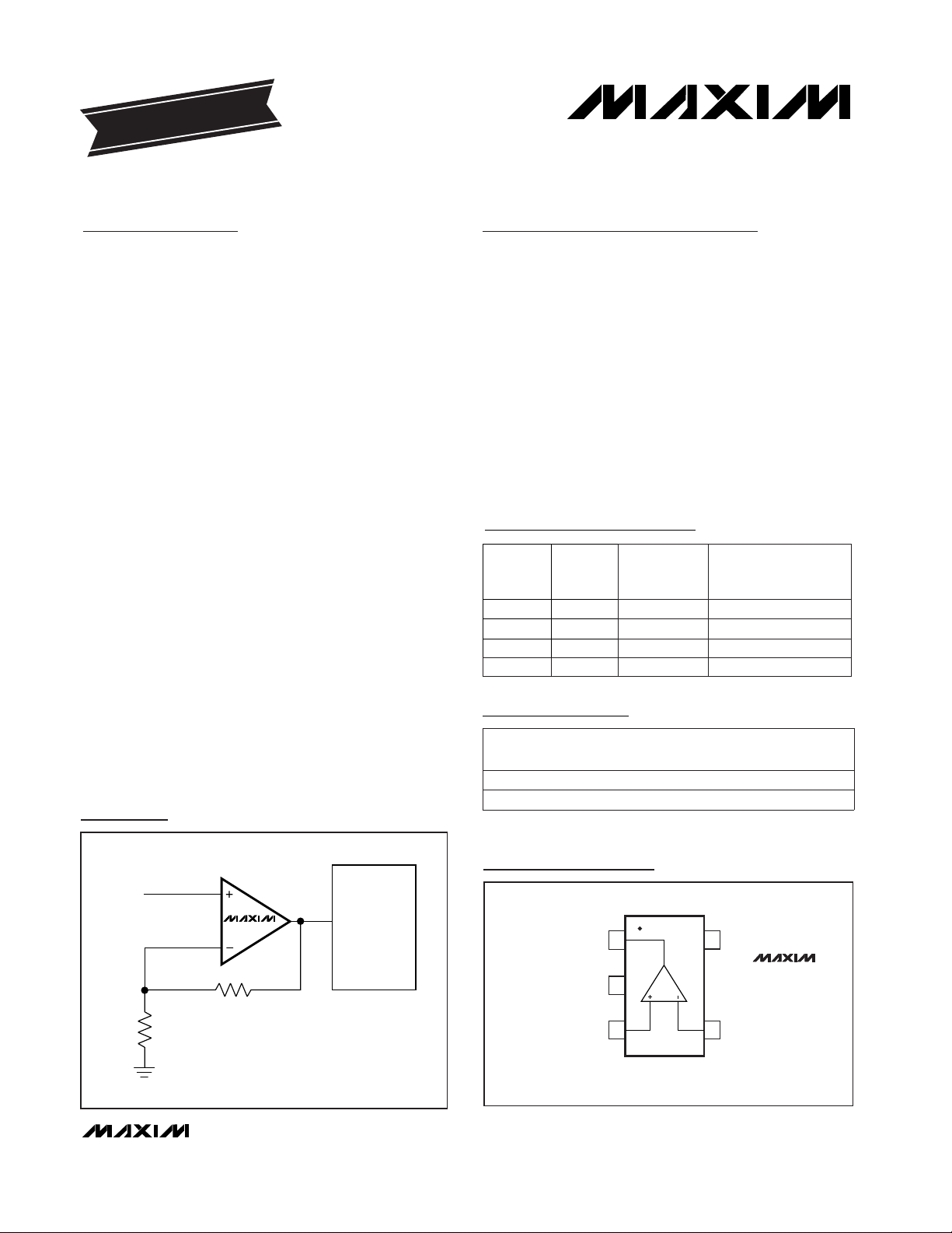
MAX4304
8 to 16-BIT
HIGH-SPEED
ADC
INPUT
330Ω
ADC BUFFER WITH GAIN (A
VCL
= 2V/V)
330Ω
Typical Application Circuit
19-4757; Rev 3; 10/98
PART
MAX4104ESA
MAX4104EUK-T -40°C to +85°C
-40°C to +85°C
TEMP. RANGE
PIN-
PACKAGE
8 SO
5 SOT23-5
EVALUATION KIT MANUAL
FOLLOWS DATA SHEET
Ordering Information
Selector Guide
SOT
TOP MARK
—
ACCO
PART
MAX4104
MAX4304
MAX4105 5
2
1
MINIMUM
STABLE
GAIN (V/V)
BANDWIDTH
(MHz)
625
740
410
MAX4305 10 340
PIN-PACKAGE
5-pin SOT23, 8-pin SO
5-pin SOT23, 8-pin SO
5-pin SOT23, 8-pin SO
5-pin SOT23, 8-pin SO
Pin Configurations
Pin Configurations continued at end of data sheet.
Ordering Information continued at end of data sheet.
TOP VIEW
15V
OUT
2
V
EE
34
SOT23-5
CC
MAX4104
MAX4105
MAX4304
MAX4305
IN-IN+
Page 2
MAX4104/MAX4105/MAX4304/MAX4305
740MHz, Low-Noise, Low-Distortion
Op Amps in SOT23-5
2 _______________________________________________________________________________________
ABSOLUTE MAXIMUM RATINGS
DC ELECTRICAL CHARACTERISTICS
(VCC= +5V, VEE= -5V, VCM= 0, RL= 100kΩ, TA= T
MIN
to T
MAX
, unless otherwise noted. Typical values are at TA= +25°C.)
Stresses beyond those listed under “Absolute Maximum Ratings” may cause permanent damage to the device. These are stress ratings only, and functional
operation of the device at these or any other conditions beyond those indicated in the operational sections of the specifications is not implied. Exposure to
absolute maximum rating conditions for extended periods may affect device reliability.
Supply Voltage (VCCto VEE)................................................+12V
Voltage on Any Pin to Ground..........(V
EE
- 0.3V) to (VCC+ 0.3V)
Short-Circuit Duration (V
OUT
to GND)........................Continuous
Continuous Power Dissipation (T
A
= +70°C)
5-pin SOT23 (derate 7.1mW/°C above +70°C)...........571mW
8-pin SO (derate 5.9mW/°C above +70°C).................471mW
Operating Temperature Range ...........................-40°C to +85°C
Storage Temperature Range.............................-65°C to +150°C
Lead Temperature (soldering, 10sec).............................+300°C
V
OUT
= 0
RL= short to ground
Guaranteed by PSRR test
RL= 30Ω
RL= 100kΩ
VCC= 3.5V to 5.5V
-2.8V ≤ VCM≤ 4.1V
-2.8V ≤ V
OUT
≤ 2.8V, RL= 100Ω
V
OUT
= 0
Guaranteed by CMRR test
Either input
-0.8V ≤ VIN≤ 0.8V
VEE= -3.5V to -5.5V
CONDITIONS
Ω9Z
OUT
Open-Loop Output Impedance
mA80I
SC
Short-Circuit Output Current
mA±53 ±70I
OUT
Output Current Drive
±3.0 -3.5 to +3.4
V
±3.5 -3.7 to +3.8
V
OUT
Output Voltage Swing
dB55 65A
VOL
Open-Loop Gain
mA20 27I
S
Quiescent Supply Current
dB55 65PSRR-
Negative Power-Supply
Rejection Ratio
mV
1 6
V
OS
V±3.5 ±5 ±5.5VCC/V
EE
Operating Supply Voltage
Range
dB75 85PSSR+
Positive Power-Supply Rejection
Ratio
dB80 95CMRRCommon-Mode Rejection Ratio
V-2.8 +4.1V
CM
Input Common-Mode Voltage
Range
MΩ1.5R
IN
Common-Mode Input
Resistance
1 8
µV/°CTCV
OS
Input Offset-Voltage Drift
µA32 70I
B
kΩ6R
IN
Differential Input Resistance
UNITSMIN TYP MAXSYMBOLPARAMETER
Input Offset Voltage
Input Bias Current
MAX4_0_EUK
2.5
MAX4_0_ESA
Input Offset Current µA0.5 5.0I
OS
RL= 100Ω
Page 3
MAX4104/MAX4105/MAX4304/MAX4305
740MHz, Low-Noise, Low-Distortion
Op Amps in SOT23-5
_______________________________________________________________________________________ 3
AC ELECTRICAL CHARACTERISTICS
(VCC= +5V, VEE= -5V, VCM= 0, RL= 100Ω; AV= +1V/V for MAX4104, +2V/V for MAX4304, +5V/V for MAX4105, +10V/V for MAX4305;
T
A
= +25°C; unless otherwise noted.)
CONDITIONS
MHz
625
BW
(-3dB)
-3dB Bandwidth
UNITSMIN TYP MAXSYMBOLPARAMETER
20
V
OUT
= 2Vp-p
f = 1MHz
f = 10MHz
f = 1MHz
Ω1Z
OUT
Output Impedance
pA/√Hz
3.1i
n
Input Current Noise Density
nV/√Hz
2.1e
n
Input Voltage Noise Density
nst
S
Settling Time to 0.1%
%
0.01
DGDifferential Gain Error
V
OUT
= 100mVp-p
MAX4104
MAX4304
MAX4105
MAX4305 340
410
740
MAX4305
MHz
100
BW
(0.1)
0.1dB Bandwidth
MAX4104
V
OUT
= 100mVp-p
MAX4304
MAX4105
70
80
60
MAX4305
MHz
115
FPBWFull-Power Bandwidth
MAX4104
V
OUT
= 2Vp-p
MAX4304
MAX4105
320
370
285
MAX4305
V/µs
400
SRSlew Rate
MAX4104
V
OUT
= 2Vp-p
MAX4304
MAX4105
1400
1400
1000
to 0.1%
25to 0.01%
-88
V
OUT
=2Vp-p
fC = 5MHz
-67fC = 20MHz
dBcSFDR
Spurious-Free
Dynamic Range
-74fC = 5MHz
-61fC = 20MHz
MAX4104/
MAX4304
MAX4105/
MAX4305
MAX4104/MAX4304
NTSC, RL= 150Ω
MAX4105/MAX4305 0.02
MAX4105/MAX4305
MAX4104/MAX4304
NTSC, RL= 150Ω degrees
0.02
0.01
DPDifferential Phase Error
Page 4
MAX4104/MAX4105/MAX4304/MAX4305
740MHz, Low-Noise, Low-Distortion
Op Amps in SOT23-5
4 _______________________________________________________________________________________
__________________________________________Typical Operating Characteristics
(VCC= +5V, V
EE
= -5V, RF= 330Ω, RL= 100Ω, TA= +25°C, unless otherwise noted.)
5
4
-5
100k 1M 10M 100M 1G
MAX4104
SMALL-SIGNAL GAIN
vs. FREQUENCY (A
VCL
= +1)
-3
-4
FREQUENCY (Hz)
GAIN (dB)
-1
-2
1
0
3
2
MAX4104 TOC01
V
OUT
= 100mVp-p
5
4
-5
100k 1M 10M 100M 1G
MAX4304
SMALL-SIGNAL GAIN
vs. FREQUENCY (A
VCL
= +2)
-3
-4
FREQUENCY (Hz)
NORMALIZED GAIN (dB)
-1
-2
1
0
3
2
MAX4104 TOC 2
V
OUT
= 100mVp-p
5
4
-5
100k 1M 10M 100M 1G
MAX4105
SMALL-SIGNAL GAIN
vs. FREQUENCY (A
VCL
= +5)
-3
-4
FREQUENCY (Hz)
NORMALIZED GAIN (dB)
-1
-2
1
0
3
2
MAX4104 TOC 3
V
OUT
= 100mVp-p
5
4
-5
100k 1M 10M 100M 1G
MAX4305
SMALL-SIGNAL GAIN
vs. FREQUENCY (A
VCL
= +10)
-3
-4
FREQUENCY (Hz)
NORMALIZED GAIN (dB)
-1
-2
1
0
3
2
MAX4104 TOC 4
V
OUT
= 100mVp-p
0.5
0.4
-0.5
100k 1M 10M 100M 1G
MAX4105
GAIN FLATNESS
vs. FREQUENCY (A
VCL
= +5)
-0.3
-0.4
FREQUENCY (Hz)
NORMALIZED GAIN (dB)
-0.1
-0.2
0.1
0
0.3
0.2
MAX4104 TOC 7
V
OUT
= 100mVp-p
0.5
0.4
-0.5
100k 1M 10M 100M 1G
MAX4104
GAIN FLATNESS
vs. FREQUENCY (A
VCL
= +1)
-0.3
-0.4
FREQUENCY (Hz)
GAIN (dB)
-0.1
-0.2
0.1
0
0.3
0.2
MAX4104 TOC 5
V
OUT
= 100mVp-p
0.5
0.4
-0.5
100k 1M 10M 100M 1G
MAX4304
GAIN FLATNESS
vs. FREQUENCY (A
VCL
= +2)
-0.3
-0.4
FREQUENCY (Hz)
NORMALIZED GAIN (dB)
-0.1
-0.2
0.1
0
0.3
0.2
MAX4104 TOC 6
V
OUT
= 100mVp-p
0.5
0.4
-0.5
100k 1M 10M 100M 1G
MAX4305
GAIN FLATNESS
vs. FREQUENCY (A
VCL
= +10)
-0.3
-0.4
FREQUENCY (Hz)
NORMALIZED GAIN (dB)
-0.1
-0.2
0.1
0
0.3
0.2
MAX4104 TOC 8
V
OUT
= 100mVp-p
5
4
-5
100k 1M 10M 100M 1G
MAX4104
LARGE-SIGNAL GAIN
vs. FREQUENCY (A
VCL
= +1)
-3
-4
FREQUENCY (Hz)
GAIN (dB)
-1
-2
1
0
3
2
MAX4104 TOC9
V
OUT
= 2Vp-p
Page 5

MAX4104/MAX4105/MAX4304/MAX4305
740MHz, Low-Noise, Low-Distortion
Op Amps in SOT23-5
_______________________________________________________________________________________
5
5
4
-5
100k 1M 10M 100M 1G
MAX4304
LARGE-SIGNAL GAIN
vs. FREQUENCY (A
VCL
= +2)
-3
-4
FREQUENCY (Hz)
NORMALIZED GAIN (dB)
-1
-2
1
0
3
2
MAX4104 TOC10
V
OUT
= 2Vp-p
5
4
-5
100k 1M 10M 100M 1G
MAX4105
LARGE-SIGNAL GAIN
vs. FREQUENCY (A
VCL
= +5)
-3
-4
FREQUENCY (Hz)
NORMALIZED GAIN (dB)
-1
-2
1
0
3
2
MAX4104 TOC 11
V
OUT
= 2Vp-p
5
4
-5
100k 1M 10M 100M 1G
MAX4305
LARGE-SIGNAL GAIN
vs. FREQUENCY (A
VCL
= +10)
-3
-4
FREQUENCY (Hz)
NORMALIZED GAIN (dB)
-1
-2
1
0
3
2
MAX4104 TOC12
V
OUT
= 2Vp-p
0
-10
-100
-90
100k 1M 10M 100M 1G
POSITIVE POWER-SUPPLY REJECTION
vs. FREQUENCY
-80
-70
MAX4104 TOCM
FREQUENCY (Hz)
POWER-SUPPLY REJECTION (dB)
-50
-60
-30
-40
-20
10 100 100k 1M 10M
FREQUENCY (Hz)
1k 10k1
100
10
1
VOLTAGE NOISE DENSITY vs. FREQUENCY
(INPUT REFERRED)
MAX4104 TOC-P
VOLTAGE NOISE DENSITY (nV/√Hz)
20
10
-80
-70
100k 1M 10M 100M 1G
NEGATIVE POWER-SUPPLY REJECTION
vs. FREQUENCY
-60
-50
MAX4104 TOCN
FREQUENCY (Hz)
POWER-SUPPLY REJECTION (dB)
-30
-40
-10
-20
0
0
-10
-100
10k 1M 10M 100M100k 1G
COMMON-MODE REJECTION
vs. FREQUENCY
-80
-90
MAX4104 TOCO
FREQUENCY (Hz)
CMR (dB)
-60
-70
-40
-50
-20
-30
10 100 100k 1M 10M
FREQUENCY (Hz)
1k 10k1
100
10
1
CURRENT NOISE DENSITY vs. FREQUENCY
(INPUT REFERRED)
CURRENT NOISE DENSITY (pA/√Hz)
MAX4104 TOC-Q
1000
0.01
100k 1M 10M 100M 1G
CLOSED-LOOP OUTPUT IMPEDANCE
vs. FREQUENCY
0.1
MAX4104 TOC-R
FREQUENCY (Hz)
OUTPUT IMPEDANCE (Ω)
1
10
100
Typical Operating Characteristics (continued)
(VCC= +5V, V
EE
= -5V, RF= 330Ω, RL= 100Ω, TA= +25°C, unless otherwise noted.)
Page 6

MAX4104/MAX4105/MAX4304/MAX4305
740MHz, Low-Noise, Low-Distortion
Op Amps in SOT23-5
6 _______________________________________________________________________________________
Typical Operating Characteristics (continued)
(VCC= +5V, V
EE
= -5V, RF= 330Ω, RL= 100Ω, TA= +25°C, unless otherwise noted.)
0 100
0 100
MAX4104/MAX4304
DIFFERENTIAL GAIN AND PHASE
-0.015
0.000
-0.010
0.005
-0.005
0.010
0.015
-0.005
0.000
0.005
IRE
DIFF PHASE (deg)
DIFF GAIN (%)
MAX4104 TOC-S
RL = 150Ω
RL = 150Ω
-0.005
0 100
0 100
MAX4105/MAX4305
DIFFERENTIAL GAIN AND PHASE
-0.01
0.010
0.005
0.000
0.00
0.015
0.01
0.020
0.02
0.025
0.03
IRE
DIFF PHASE (deg)
DIFF GAIN (%)
MAX4104 TOC T
RL = 150Ω
RL = 150Ω
0
-100
100k 1M 10M 100M
MAX4104/MAX4304
HARMONIC DISTORTION vs. FREQUENCY
-80
MAX4104 TOC-U
FREQUENCY (Hz)
HARMONIC DISTORTION (dBc)
-60
-40
-20
-10
-90
-70
-50
-30
3RD HARMONIC
2ND HARMONIC
V
OUT
= 2Vp-p
0
-100
100k 1M 10M 100M
MAX4105/MAX4305
HARMONIC DISTORTION vs. FREQUENCY
-80
MAX4104 TOC-V
FREQUENCY (Hz)
DISTORTION (dBc)
-60
-40
-20
-10
-90
-70
-50
-30
3RD HARMONIC
2ND HARMONIC
V
OUT
= 2Vp-p
-100
-80
-90
-60
-70
-40
-50
-30
-10
-20
0
0.5 1.5 2.0 2.51.0 3.0 3.5 4.0
MAX4104/MAX4304
HARMONIC DISTORTION
vs. OUTPUT SWING
MAX4104 TOC-Y
OUTPUT SWING (Vp-p)
HARMONIC DISTORTION (dBc)
3RD HARMONIC
2ND HARMONIC
f = 5MHz
-100
-80
-90
-60
-70
-40
-50
-30
-10
-20
0
0 200 300 400100 500 600 700 900800 1k
MAX4104/MAX4304
HARMONIC DISTORTION vs. LOAD
MAX4104 TOC-W
LOAD (Ω)
HARMONIC DISTORTION (dBc)
3RD HARMONIC
2ND HARMONIC
f = 5MHz
V
OUT
= 2Vp-p
-100
-80
-90
-60
-70
-40
-50
-30
-10
-20
0
0 200 300 400100 500 600 700 900800 1k
MAX4105/MAX4305
HARMONIC DISTORTION vs. LOAD
MAX4104 TOC-X
LOAD (Ω)
HARMONIC DISTORTION (dBc)
3RD HARMONIC
2ND HARMONIC
f = 5MHz
V
OUT
= 2Vp-p
-100
-80
-90
-60
-70
-40
-50
-30
-10
-20
0
0.5 1.5 2.0 2.51.0 3.0 3.5 4.0
MAX4105/MAX4305
HARMONIC DISTORTION
vs. OUTPUT SWING
MAX4104 TOC-Z
OUTPUT SWING (Vp-p)
HARMONIC DISTORTION (dBc)
3RD HARMONIC
2ND HARMONIC
f = 5MHz
1
3
2
5
4
7
6
8
0 100 15050 200 250 300 350 400
OUTPUT SWING vs. LOAD RESISTANCE
MAX4104 TOCAA
LOAD RESISTANCE (Ω)
OUTPUT SWING (Vp-p)
Page 7

MAX4104/MAX4105/MAX4304/MAX4305
740MHz, Low-Noise, Low-Distortion
Op Amps in SOT23-5
_______________________________________________________________________________________
7
-3.0
-2.0
0.0
-1.0
1.5
2.0
3.0
-2.5
-0.5
-1.5
1.0
0.5
2.5
-40 10-15 35 60 85
INPUT OFFSET VOLTAGE
vs. TEMPERATURE
MAX4104 TOCBB
TEMPERATURE (°C)
INPUT OFFSET VOLTAGE (mV)
-3
-1
-2
1
0
3
2
4
-40 10-15 35 60 85
INPUT OFFSET CURRENT
vs. TEMPERATURE
MAX4104 TOC-CC
TEMPERATURE (°C)
INPUT OFFSET CURRENT (µA)
30
31
33
32
34
35
-40 10-15 35 60 85
INPUT BIAS CURRENT
vs. TEMPERATURE
MAX4104 TOC-DD
TEMPERATURE (°C)
INPUT BIAS CURRENT (µA)
15
18
17
16
19
20
21
22
23
24
25
9.0 9.5 10.0 10.5 11.0
SUPPLY CURRENT
vs. SUPPLY VOLTAGE
MAX4104 TOC-FF
SUPPLY VOLTAGE (V)
SUPPLY CURRENT (mA)
15
18
17
16
19
20
21
22
23
24
25
-40 10-15 35 60 85
SUPPLY CURRENT
vs. TEMPERATURE
MAX4104 TOC-EE
TEMPERATURE (°C)
SUPPLY CURRENT (mA)
-50mV
+50mV
OUT
IN
-25mV
GND
GND
+25mV
10ns/div
MAX4304
SMALL-SIGNAL PULSE RESPONSE
(A
V
= +2)
MAX4104 TOCII
3.2
3.3
3.4
3.5
3.6
3.7
3.8
3.9
4.0
-40 -15 10 35 60 85
POSITIVE OUTPUT VOLTAGE SWING
vs. TEMPERATURE
MAX4104 TOC-GG
TEMPERATURE (°C)
VOLTAGE SWING (V)
RL = 100kΩ
RL = 100kΩ
-50mV
OUT
+50mV
+50mV
-50mV
IN
GND
GND
10ns/div
MAX4104
SMALL-SIGNAL PULSE RESPONSE
(A
V
= +1)
MAX4104 TOCHH
-50mV
OUT
+50mV
-10mV
GND
GND
+10mV
IN
10ns/div
MAX4105
SMALL-SIGNAL PULSE RESPONSE
(A
V
= +5)
MAX4104 TOCJJ
Typical Operating Characteristics (continued)
(VCC= +5V, V
EE
= -5V, RF= 330Ω, RL= 100Ω, TA= +25°C, unless otherwise noted.)
Page 8

MAX4104/MAX4105/MAX4304/MAX4305
740MHz, Low-Noise, Low-Distortion
Op Amps in SOT23-5
8 _______________________________________________________________________________________
Typical Operating Characteristics (continued)
(VCC= +5V, V
EE
= -5V, RF= 330Ω, RL= 100Ω, TA= +25°C, unless otherwise noted.)
-1V
OUT
+1V
+1V
IN
-1V
GND
GND
10ns/div
MAX4104
LARGE-SIGNAL PULSE RESPONSE
(A
V
= +1)
MAX4104 TOCLL
-1V
OUT
+1V
+500mV
-500mV
IN
GND
GND
10ns/div
MAX4305
LARGE-SIGNAL PULSE RESPONSE
(A
V
= +2)
MAX4104 TOCMM
-1V
OUT
IN
+1V
+200mV
-200mV
GND
GND
10ns/div
MAX4105
LARGE-SIGNAL PULSE RESPONSE
(A
V
= +5)
MAX4104 TOCNN
-1V
+1V
OUT
+100mV
IN
-100mV
GND
GND
10ns/div
MAX4305
LARGE-SIGNAL PULSE RESPONSE
(A
V
= +10)
MAX4104 TOCOO
-50mV
+50mV
OUT
IN
-5mV
GND
GND
+5mV
10ns/div
MAX4305
SMALL-SIGNAL PULSE RESPONSE
(A
V
= +10)
MAX4104 TOCKK
Page 9

_______________Detailed Description
The MAX4104/MAX4105/MAX4304/MAX4305 are ultrahigh-speed, low-noise amplifiers featuring -3dB bandwidths up to 880MHz, 0.1dB gain flatness up to
100MHz, and low differential gain and phase errors of
0.01% and 0.01°, respectively. These devices operate
on dual power supplies ranging from ±3.5V to ±5.5V
and require only 20mA of supply current.
The MAX4104/MAX4304/MAX4105/MAX4305 are optimized for minimum closed-loop gains of +1V/V, +2V/V,
+5V/V and +10V/V (respectively) with corresponding
-3dB bandwidths of 880MHz, 730MHz, 430MHz, and
350MHz. Each device in this family features a low input
voltage noise density of only 2.1nV/√Hz (at 1MHz), an
output current drive of ±70mA, and spurious-free
dynamic range as low as -88dBc (5MHz, RL= 100Ω).
___________Applications Information
Layout and Power-Supply Bypassing
The MAX4104/MAX4105/MAX4304/MAX4305 have an
extremely high bandwidth, and consequently require
careful board layout, including the possible use of
constant-impedance microstrip or stripline techniques.
To realize the full AC performance of these high-speed
amplifiers, pay careful attention to power-supply
bypassing and board layout. The PC board should
have at least two layers: a signal and power layer on
one side, and a large, low-impedance ground plane on
the other side. The ground plane should be as free of
voids as possible. With multilayer boards, locate the
ground plane on a layer that incorporates no signal or
power traces.
Regardless of whether or not a constant-impedance
board is used, it is best to observe the following guidelines when designing the board:
1) Do not use wire-wrapped boards (they are much too
inductive) or breadboards (they are much too
capacitive).
2) Do not use IC sockets. IC sockets increase reac tances.
3) Keep signal lines as short and straight as possible.
Do not make 90° turns; round all corners.
4) Observe high-frequency bypassing techniques to
maintain the amplifier’s accuracy and stability.
5) Bear in mind that, in general, surface-mount components have shorter bodies and lower parasitic reactance, resulting in greatly improved high-frequency
performance over through-hole components.
The bypass capacitors should include 1nF and 0.1µF
ceramic surface-mount capacitors between each supply pin and the ground plane, located as close to the
package as possible. Optionally, place a 10µF tantalum
capacitor at the power supply pins’ point of entry to the
PC board to ensure the integrity of incoming supplies.
The power-supply trace should lead directly from the
tantalum capacitor to the V
CC
and VEEpins. To minimize parasitic inductance, keep PC traces short and
use surface-mount components.
Input termination resistors and output back-termination
resistors, if used, should be surface-mount types, and
should be placed as close to the IC pins as possible.
DC and Noise Errors
The MAX4104/MAX4105/MAX4304/MAX4305 output
offset voltage, V
OUT
(Figure 1), can be calculated with
the following equation:
V
OUT
= [VOS+ (IB+x RS) + (IB-x (R
F
||
RG))] [1 + RF/ RG]
where:
VOS= input offset voltage (in volts)
1 + RF/RG= amplifier closed-loop gain (dimensionless)
IB+= noninverting input bias current (in amps)
IB-= inverting input bias current (in amps)
RG= gain-setting resistor (in ohms)
RF= feedback resistor (in ohms)
RS= source resistor at noninverting input (in ohms)
The following equation represents output noise density:
e 1
R
R
i x R i x R R e
n(OUT)
F
G
n S
2
n F G
2
n
2
||= +
( )
+
( )
+
MAX4104/MAX4105/MAX4304/MAX4305
740MHz, Low-Noise, Low-Distortion
Op Amps in SOT23-5
_______________________________________________________________________________________ 9
_____________________Pin Description
SOT23-5 SO
OUT
V
CC
V
EE
IN+
IN-
N.C.
NAME
Amplifier Output61
Positive Power Supply75
Negative Power Supply 42
Amplifier Noninverting
Input
33
Amplifier Inverting Input24
Not internally connected.1, 5, 8
—
FUNCTION
PIN
Page 10

MAX4104/MAX4105/MAX4304/MAX4305
where:
in= input current noise density (in pA/√Hz)
en= input voltage noise density (in nV/√Hz)
The MAX4104/MAX4105/MAX4304/MAX4305 have a
very low, 2.1nV/√Hz input voltage noise density and
3.1pA/√Hz input current noise density.
An example of DC-error calculations, using the
MAX4304 typical data and the typical operating circuit
with RF= RG= 330Ω (RF|| RG= 165Ω) and RS= 50Ω
gives:
Calculating total output noise in a similar manner yields
the following:
With a 200MHz system bandwidth, this calculates to
60.8µV
RMS
(approximately 365µVp-p, using the six-
sigma calculation).
ADC Input Buffers
Input buffer amplifiers can be a source of significant
error in high-speed ADC applications. The input buffer
is usually required to rapidly charge and discharge the
ADC’s input, which is often capacitive. In addition, the
input impedance of a high-speed ADC often changes
very rapidly during the conversion cycle—a condition
that demands an amplifier with very low output impedance at high frequencies to maintain measurement
accuracy. The combination of high-speed, fast slew
rate, low noise, and low-distortion available in the
MAX4104/MAX4105/MAX4304/MAX4305 makes them
ideally suited for use as buffer amplifiers in high-speed
ADC applications.
Video Line Driver
The MAX4104/MAX4105/MAX4304/MAX4305 are optimized to drive coaxial transmission lines when the
cable is terminated at both ends, as shown in Figure 2.
To minimize reflections and maximize power transfer,
select the termination resistors to match the characteristic impedance of the transmission line. Cable frequency response can cause variations in the flatness of the
signal.
Driving Capacitive Loads
The MAX4104/MAX4105/MAX4304/MAX4305 provide
maximum AC performance when driving no output load
capacitance. This is the case when driving a correctly
terminated transmission line (i.e., a back-terminated
cable).
In most amplifier circuits, driving a large load capacitance increases the chance of oscillations occurring.
The amplifier’s output impedance and the load capacitor combine to add a pole and excess phase to the
loop response. If the pole’s frequency is low enough
and phase margin is degraded sufficiently, oscillations
may result.
A second concern when driving capacitive loads originates from the amplifier’s output impedance, which
e
x x x x x
e nV Hz
n OUT
n OUT
( )
( )
. . .
.
=
+
[ ]
+
+
=
− − −
1 1 3 1 10 50 3 1 10 165 2 1 10
4 3
12
2
12
2
9
2
V 32 x 10 50 32 x 10 165 1 x 10 1 1
V 15.8mV
OUT
6 6 3
OUT
=
( )
+
( )
+
+
[ ]
=
− − −
Ω
740MHz, Low-Noise, Low-Distortion
Op Amps in SOT23-5
10 ______________________________________________________________________________________
MAX4104
MAX4105
MAX4304
MAX4305
R
G
FB
I
B-
I
B+
IN
V
OUT
OUT
R
S
R
F
Figure 1. Output Offset Voltage Figure 2. Video Line Driver
MAX4104
MAX4105
MAX4304
MAX4305
R
G
IN-
IN+
OUT
R
L
75Ω
R
T
75Ω
R
T
75Ω
75Ω CABLE
75Ω CABLE
R
F
Page 11

appears inductive at high frequencies. This inductance
forms an L-C resonant circuit with the capacitive load,
which causes peaking in the frequency response and
degrades the amplifier’s phase margin.
The MAX4104/MAX4105/MAX4304/MAX4305 drive
capacitive loads up to 10pF without oscillation.
However, some peaking may occur in the frequency
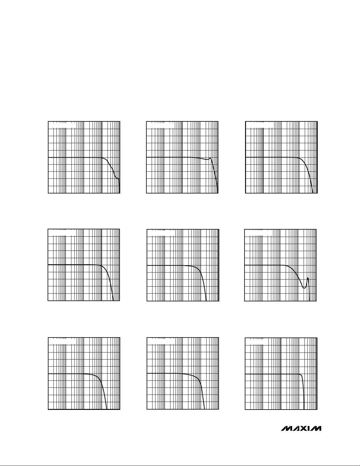
domain (Figure 3). To drive larger capacitance loads or
to reduce ringing, add an isolation resistor between the
amplifier’s output and the load (Figure 4).
The value of R
ISO
depends on the circuit’s gain and the
capacitive load (Figure 5). Figure 6 shows the
MAX4104/MAX4105/MAX4304/MAX4305 frequency
response with the isolation resistor and a capacitive
load. With higher capacitive values, bandwidth is dominated by the RC network formed by R
ISO
and CL; the
bandwidth of the amplifier itself is much higher. Also
note that the isolation resistor forms a divider that
decreases the voltage delivered to the load.
Maxim’s High-Speed Evaluation Boards
The MAX4104 evaluation kit manual shows a suggested layout for Maxim’s high-speed, single-amplifier evaluation boards. This board was developed using the
techniques described previously (
see Layout and
Power-Supply Bypassing
section). The smallest available surface-mount resistors were used for the feedback and back-termination resistors to minimize the
MAX4104/MAX4105/MAX4304/MAX4305
740MHz, Low-Noise, Low-Distortion
Op Amps in SOT23-5
______________________________________________________________________________________ 11
Figure 3a. MAX4104 Frequency Response with Capacitive
Load and No Isolation Resistor
30
25
-20
100k 1M 10M 100M 1G
-10
-15
FREQUENCY (Hz)
GAIN (dB)
0
-5
10
5
20
15
CL = 10pF
CL = 5pF
CL = 15pF
Figure 3b. MAX4304 Frequency Response with Capacitive
Load and No Isolation Resistor
Figure 3d. MAX4305 Frequency Response with Capacitive
Load and No Isolation Resistor
Figure 3c. MAX4105 Frequency Response with Capacitive
Load and No Isolation Resistor
30
25
-20
100k 1M 10M 100M 1G
-10
-15
FREQUENCY (Hz)
NORMALIZED GAIN (dB)
0
-5
10
5
20
15
CL = 5pF
CL = 15pF
CL = 10pF
25
20
15
10
5
0
-5
-10
NORMALIZED GAIN (dB)
-15
-20
-25
100k 1M 10M 100M 1G
CL = 5pF
FREQUENCY (Hz)
CL = 15pF
CL = 10pF
25
20
15
10
5
0
-5
-10
NORMALIZED GAIN (dB)
-15
-20
-25
100k 1M 10M 100M 1G
FREQUENCY (Hz)
CL = 15pF
CL = 10pF
CL = 5pF
Page 12

MAX4104/MAX4105/MAX4304/MAX4305
distance from the IC to these resistors, thus reducing
the capacitance associated with longer lead lengths.
SMA connectors were used for best high-frequency
performance. Because distances are extremely short,
performance is unaffected by the fact that inputs and
outputs do not match a 50Ω line. However, in applications that require lead lengths greater than 1/4 of the
wavelength of the highest frequency of interest,
constant-impedance traces should be used.
Fully assembled evaluation boards are available for the
MAX4104 in an 8-pin SO package.
740MHz, Low-Noise, Low-Distortion
Op Amps in SOT23-5
12 ______________________________________________________________________________________
MAX4104
MAX4105
MAX4304
MAX4305
R
G
IN-
IN+
R
ISO
OUT
R
F
C
L
R
L
Figure 5. Optimal Isolation Resistor (R
ISO
) vs. Capacitive
Load
4
3
-6
100k 1M 10M 100M 1G
-4
-5
FREQUENCY (Hz)
GAIN (dB)
-2
-3
0
-1
2
1
CL = 47pF
MAX4104/MAX4304
R
ISO
= 15Ω
CL = 83pF
CL = 68pF
Figure 6. Frequency Responses vs. Capacitive Load with 15
Ω
Isolation Resistor
Figure 4. Using an Isolation Resistor (R
ISO
) for High Capacitive
Loads
Chip Information
TRANSISTOR COUNT: 44
SUBSTRATE CONNECTED TO V
EE
Ordering Information (continued)
*
Future product—contact factory for availability.
PART
MAX4105ESA
-40°C to +85°C
TEMP. RANGE
PIN-
PACKAGE
8 SO
MAX4105EUK-T -40°C to +85°C 5 SOT23-5
MAX4304ESA
MAX4304EUK-T
MAX4305ESA*
-40°C to +85°C
-40°C to +85°C
-40°C to +85°C 8 SO
5 SOT23-5
8 SO
MAX4305EUK-T -40°C to +85°C 5 SOT23-5
SOT
TOP MARK
—
ACCP
—
ACCQ
—
ACCR
OUT
IN+
N.C.
V
EE
1
2
8
7
N.C.
V
CC
IN-
N.C.
MAX4304
MAX4305
MAX4104
MAX4105
SO
TOP VIEW
3
4
6
5
Pin Configurations (continued)
30
25
20
MAX4105/MAX4305
15
10
5
MAX4104/MAX4304
OPTIMAL ISLOATION RESISTOR (Ω)
0
0 10050 150 200 250
CAPACITIVE LOAD (pF)
 Loading...