Maxim MAX4103ESA, MAX4102ESA Datasheet

19-0471; Rev 0; 2/96
250MHz, Broadcast-Quality, Low-Power
Video Op Amps
_______________General Description
The MAX4102/MAX4103 op amps combine high-speed
performance and ultra-low differential gain and phase
while drawing only 5mA of supply current. The
MAX4102 is compensated for unity-gain stability, while
the MAX4103 is compensated for a closed-loop gain
(A
) of 2V/V or greater.
VCL
The MAX4102/MAX4103 deliver a 250MHz -3dB bandwidth
(MAX4102) or a 180MHz -3dB bandwidth (MAX4103).
Differential gain and phase are an ultra-low 0.002%/0.002°
(MAX4102) and 0.008%/0.003° (MAX4103), making these
amplifiers ideal for composite video applications.
These high-speed op amps have a wide output voltage
swing of ±3.4V (RL= 100Ω) and 80mA current-drive
capability.
________________________Applications
Broadcast and High-Definition TV Systems
Pulse/RF Amplifier
ADC/DAC Amplifier
____________________________Features
♦ 250MHz -3dB Bandwidth (MAX4102)
180MHz -3dB Bandwidth (MAX4103)
♦ Unity-Gain Stable (MAX4102)
♦ 350V/µs Slew Rate
♦ Lowest Differential Gain/Phase (RL= 150Ω)
MAX4102: 0.002%/0.002°
MAX4103: 0.008%/0.003°
♦ Low Distortion (SFDR 5MHz): -78dBc
♦ 100dB Open-Loop Gain
♦ High Output Drive: 80mA
♦ Low Power: 5mA Supply Current
______________Ordering Information
PART
MAX4102ESA
MAX4103ESA
TEMP. RANGE PIN-PACKAGE
-40°C to +85°C
-40°C to +85°C
8 SO
8 SO
MAX4102/MAX4103
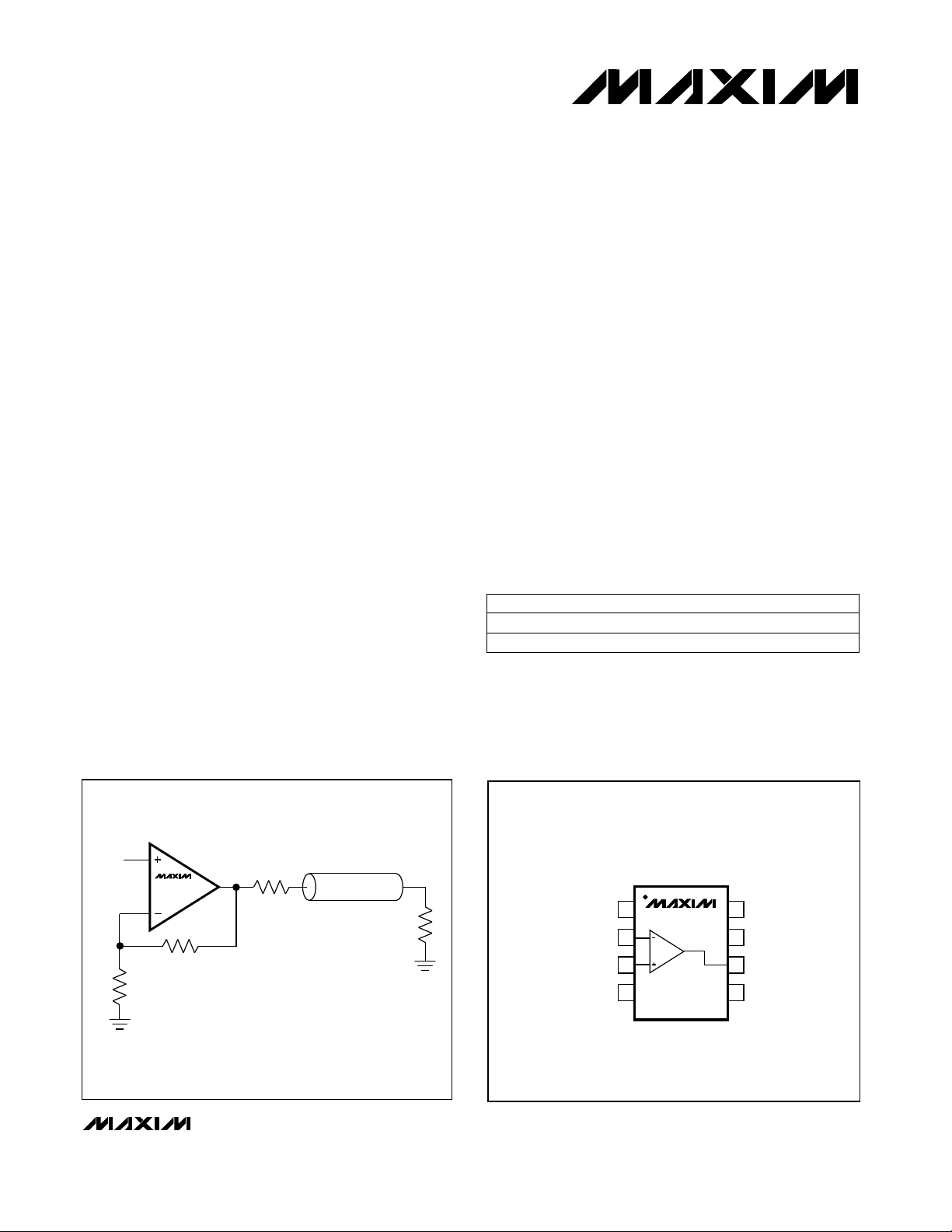
________Typical Application Circuit
INPUT
390Ω
MAX4102
MAX4103
390Ω
75Ω
75Ω
__________________Pin Configuration
TOP VIEW
N.C.
IN+
V
1
MAX4102
MAX4103
2
IN-
3
4
EE
SO
8
N.C.
V
7
CC
OUT
6
N.C.
5
VIDEO CABLE DRIVER
________________________________________________________________
Maxim Integrated Products
1
For free samples & the latest literature: http://www.maxim-ic.com, or phone 1-800-998-8800

250MHz, Broadcast-Quality, Low-Power
Video Op Amps
ABSOLUTE MAXIMUM RATINGS
Supply Voltage (VCCto VEE)..................................................12V
Voltage on Any Pin to Ground or Any Other Pin.........V
Short-Circuit Duration (V
Continuous Power Dissipation (T
SO (derate 5.88mW/°C above +70°C).........................471mW
Stresses beyond those listed under “Absolute Maximum Ratings” may cause permanent damage to the device. These are stress ratings only, and functional
operation of the device at these or any other conditions beyond those indicated in the operational sections of the specifications is not implied. Exposure to
absolute maximum rating conditions for extended periods may affect device reliability.
to GND)........................Continuous
OUT
= +70°C)
A
CC
to V
EE
DC ELECTRICAL CHARACTERISTICS
(VCC= 5V, VEE= -5V, TA= T
DC SPECIFICATIONS
Input Offset Voltage
Input Offset Voltage Drift
Input Bias Current
MAX4102/MAX4103
Input Offset Current
Common-Mode Input Resistance
Common-Mode Input Capacitance
Input Voltage Noise
Integrated Voltage Noise
Input Current Noise
Integrated Current Noise
Common-Mode Input Voltage
Open-Loop Voltage Gain
Quiescent Supply Current
Output Voltage Swing
Short-Circuit Output Current
MIN
to T
, unless otherwise noted. Typical values are at TA= +25°C.)
MAX
V
OS
OS
B
OS
INCM
INCM
e
n
i
n
CM
A
VOL
SY
V
OUT
SC
= 0V
OUT
V
= 0V
OUT
V
= 0V, V
OUT
V
OUT
Either input
Either input
f = 100kHz
f = 1MHz to 100MHz
f = 100kHz
f = 1MHz to 100MHz
VS= ±4.5V to ±5.5V
V
OUT
VIN= 0V
RL= ∞
RL = 100Ω
RL = 30Ω, TA= 0°C to +85°C
Short to ground or either supply voltage
IN
= 0V, V
IN
= ±2.0V, VCM= 0V
Operating Temperature Range
MAX4102ESA/MAX4103ESA...........................-40°C to +85°C
Storage Temperature Range.............................-65°C to +160°C
Lead Temperature (soldering, 10sec).............................+300°C
CONDITIONS
= -V
OS
= -V
OS
MAX4102
MAX4103
MAX4102
MAX4103
MAX4102
MAX4103
MAX4102
MAX4103
RL = ∞
RL = 100Ω
66 96
70 100
±3.3 ±3.7
±3.1 ±3.4
7
5
88
63
1.0
1.0
12.5
12.5
UNITSMIN TYP MAXSYMBOLPARAMETER
µV/°C5TCV
nV/√Hz
µV
pA/√Hz
nA
mV0.5 8V
µA39I
µA0.04 0.5I
MΩ5R
pF1C
RMS
RMS
V-2.5 2.5V
dB75 100CMRCommon-Mode Rejection VCM= ±2.5V
dB70 100PSRPower-Supply Rejection
dB
mA4.6 6I
V
mA65 80Output Current
mA90I
2 _______________________________________________________________________________________

250MHz, Broadcast-Quality, Low-Power
Video Op Amps
AC ELECTRICAL CHARACTERISTICS
(VCC= 5V, VEE= -5V, RL= 100Ω, A
AC SPECIFICATIONS
0.1dB Bandwidth
Settling Time
Rise/Fall Times tR, t
Differential Gain
Differential Phase DP
Input Capacitance C
Output Resistance R
Spurious-Free Dynamic Range SFDR
= +1 (MAX4102), A
VCL
SYMBOL UNITSCONDITIONS
V
BW-3dB Bandwidth
OUT
≤ 0.1V
MAX4102
MAX4103
OUT
-1V ≤ V
t
DG
s
F
OUT
10% to 90%, -2V ≤ V
10% to 90%, -50mV ≤ V
f = 3.58MHz,
RL= 150Ω
f = 3.58MHz,
RL= 150Ω
IN
f = 10MHz
OUT
fC= 5MHz,
V
= 2V
OUT
= +2 (MAX4103), TA= +25°C, unless otherwise noted.)
VCL
MIN TYP MAXPARAMETER
RMS
MAX4102
MAX4103
250
180
130
80
≤ 2V
≤ 1V ns
≤ 2V 13
OUT
≤ 50mV 1.5
OUT
to 0.1%
to 0.01%
MAX4102
MAX4103
MAX4102
MAX4103
18
30
0.002
0.008
0.002
0.003
degrees
2 pF
MAX4102
0.7
MAX4103 0.7
-78
-76
p-p
MAX4102
MAX4103
MAX4102/MAX4103
MHz
MHz
V/µsSRSlew Rate 350-2V ≤ V
ns
%
Ω
dBc
__________________________________________Typical Operating Characteristics
(VCC= 5V, VEE= -5V, RL= 100Ω, TA = +25°C, unless otherwise noted.)
= 2V/V
= 2V/V
MAX4103
IRE
IRE
100
0.004
0.002
0.000
MAX4102/03-02
-0.002
-0.004
-0.006
DIFF GAIN (%)
-0.008
-0.010
0.015
0.010
0.005
0.000
-0.005
DIFF PHASE (deg)
-0.010
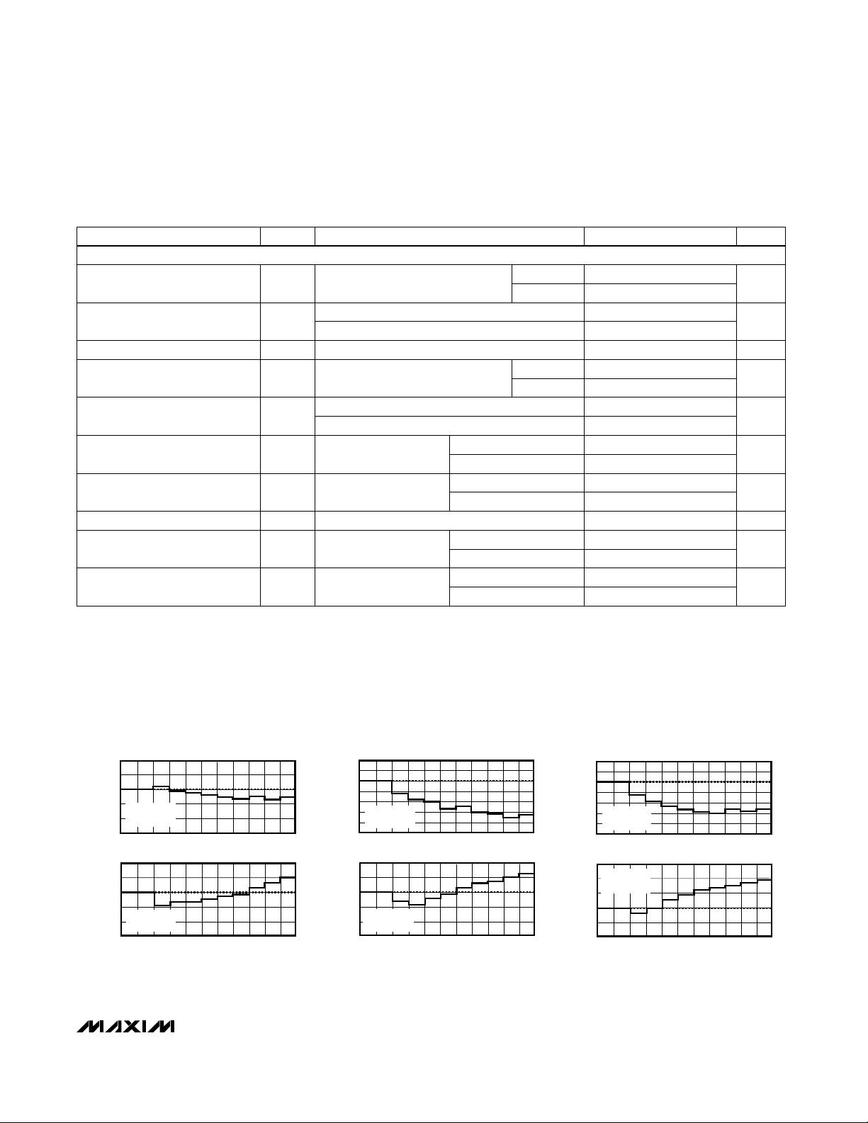
DIFFERENTIAL GAIN AND PHASE
MAX4102
RL = 75Ω
= 1V/V
A
VCL
0
RL = 75Ω
= 1V/V
A
VCL
0 100
IRE
IRE
100
DIFFERENTIAL GAIN AND PHASE
MAX4102
0.004
0.002
0.000
-0.002
RL = 150Ω
DIFF GAIN (%)
-0.004
-0.006
0.004
0.002
0.000
-0.002
-0.004
DIFF PHASE (deg)
-0.006
= 1V/V
A
VCL
0
RL = 150Ω
= 1V/V
A
VCL
0 100
IRE
IRE
_______________________________________________________________________________________ 3
100
0.004
0.002
0.000
MAX4102/03-01
-0.002
-0.004
-0.006
DIFF GAIN (%)
-0.008
-0.010
0.004
0.002
0.000
-0.002
-0.004
DIFF PHASE (deg)
-0.006
DIFFERENTIAL GAIN AND PHASE
RL = 150Ω
A
VCL
0
RL = 150Ω
A
VCL
0 100
MAX4102/03-03

250MHz, Broadcast-Quality, Low-Power
Video Op Amps
____________________________Typical Operating Characteristics (continued)
(VCC= 5V, VEE= -5V, RL= 100Ω, TA = +25°C, unless otherwise noted.)
DIFFERENTIAL GAIN AND PHASE
MAX4103
0.005
0.000
-0.005
-0.010
RL = 75Ω
DIFF GAIN (%)
-0.015
-0.020
0.020
0.015
0.010
0.005
0.000
-0.005
DIFF PHASE (deg)
-0.010
MAX4102/MAX4103
= 2V/V
A
VCL
0
RL = 75Ω
= 2V/V
A
VCL
0 100
IRE
IRE
100
MAX4102/03-04
-1
GAIN (dB)
-3
-5
MAX4102/MAX4103
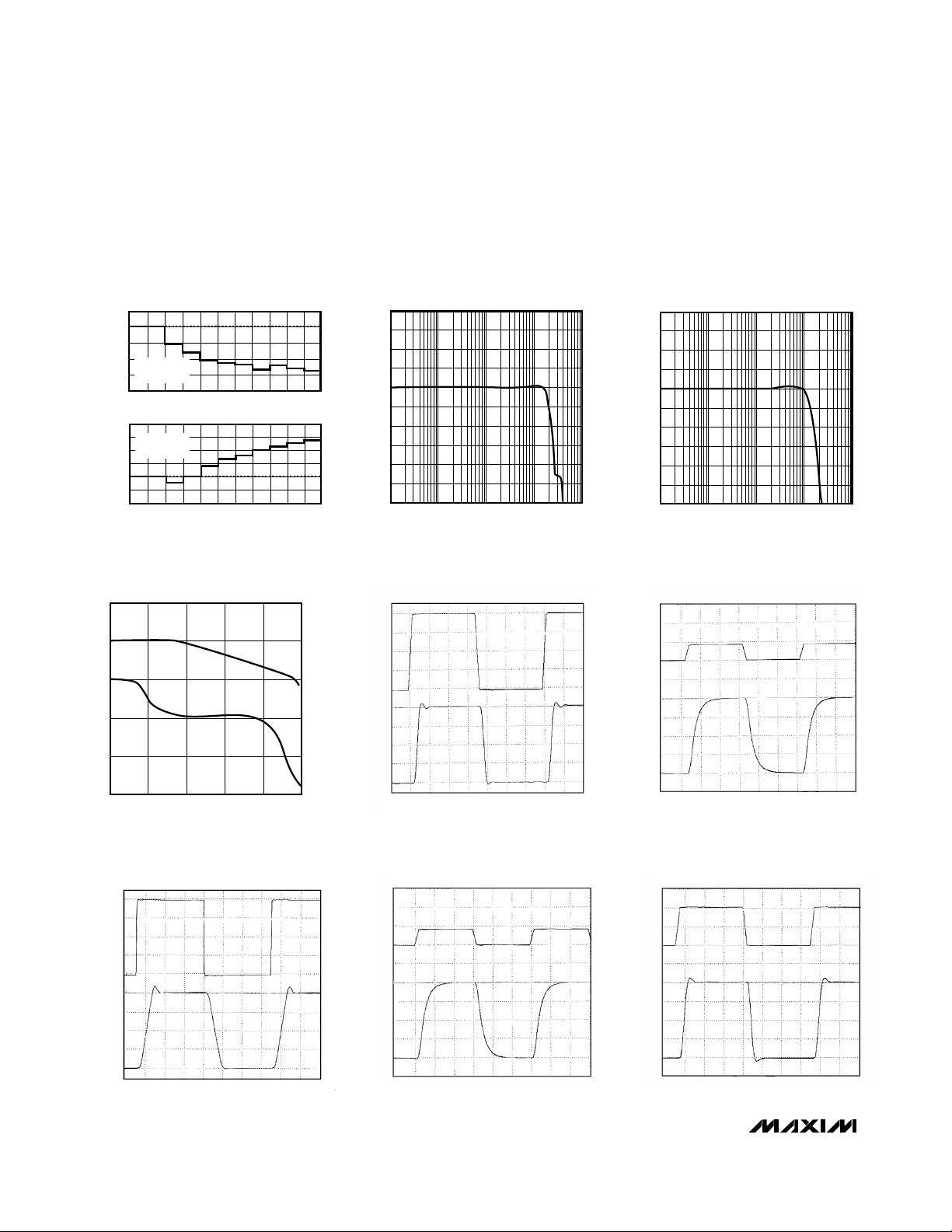
OPEN-LOOP GAIN
200
100
0
GAIN (dB)
-100
-200
AND PHASE vs. FREQUENCY
MAX4102/03-07
200
100
0
-100
-200
PHASE (degrees)
VOLTAGE (25mv/div)
SMALL-SIGNAL GAIN vs. FREQUENCY
MAX4102
(A
= +1)
4
3
2
1
0
-2
-4
-6
0.1M 10M1M 100M 1G
VCL
FREQUENCY (Hz)
MAX4102
SMALL-SIGNAL
PULSE RESPONSE (A
VCL
= +1)
IN
OUT
MAX4102/03-09
MAX4102/03-05
GAIN (dB)
GND
GND
SMALL-SIGNAL GAIN vs. FREQUENCY
MAX4103
(A
= +2)
4
3
2
1
0
-1
-2
-3
-4
-5
-6
0.1M 10M1M 100M 1G
VCL
FREQUENCY (Hz)
MAX4102
SMALL-SIGNAL
PULSE RESPONSE (A
VCL
= +5)
IN
VOLTAGE (25mv/div)
OUT
MAX4102/03-06
MAX4102/03-10
GND
GND
= +1)
MAX4102/03-11
-300
VOLTAGE (500mv/div)
GND
TIME (10ns/div)
MAX4102
LARGE-SIGNAL
PULSE RESPONSE (A
IN GND
OUT
TIME (20ns/div)
= +5)
VCL
MAX4102/03-12
GND
VOLTAGE (25mv/div)
TIME (20ns/div)
SMALL-SIGNAL
PULSE RESPONSE (A
IN GND
OUT
-300
1 10k100 1M 100M 1G
FREQUENCY (Hz)
MAX4102
LARGE-SIGNAL
PULSE RESPONSE (A
VCL
IN GND
VOLTAGE (500mv/div)
OUT
TIME (10ns/div)
4 _______________________________________________________________________________________
MAX4103
TIME (10ns/div)
VCL
= +2)
MAX4102/03-13
GND
 Loading...