

Page 1
General Description
The MAX410/MAX412/MAX414 single/dual/quad op
amps set a new standard for noise performance in
high-speed, low-voltage systems. Input voltage-noise
density is guaranteed to be less than 2.4nV/√Hz at
1kHz. A unique design not only combines low noise
with ±5V operation, but also consumes 2.5mA supply
current per amplifier. Low-voltage operation is guaranteed with an output voltage swing of 7.3V
P-P
into 2kΩ
from ±5V supplies. The MAX410/MAX412/MAX414 also
operate from supply voltages between ±2.4V and ±5V
for greater supply flexibility.
Unity-gain stability, 28MHz bandwidth, and 4.5V/µs
slew rate ensure low-noise performance in a wide variety of wideband and measurement applications. The
MAX410/MAX412/MAX414 are available in DIP and SO
packages in the industry-standard single/dual/quad op
amp pin configurations. The single comes in an ultrasmall TDFN package (3mm ✕ 3mm).
Applications
Low-Noise Frequency Synthesizers
Infrared Detectors
High-Quality Audio Amplifiers
Ultra Low-Noise Instrumentation Amplifiers
Bridge Signal Conditioning
Features
♦ Voltage Noise: 2.4nV/√Hz (max) at 1kHz
♦ 2.5mA Supply Current Per Amplifier
♦ Low Supply Voltage Operation: ±2.4V to ±5V
♦ 28MHz Unity-Gain Bandwidth
♦ 4.5V/µs Slew Rate
♦ 250µV (max) Offset Voltage (MAX410/MAX412)
♦ 115dB (min) Voltage Gain
♦ Available in an Ultra-Small TDFN Package
MAX410/MAX412/MAX414
Single/Dual/Quad, 28MHz, Low-Noise,
Low-Voltage, Precision Op Amps
________________________________________________________________ Maxim Integrated Products 1
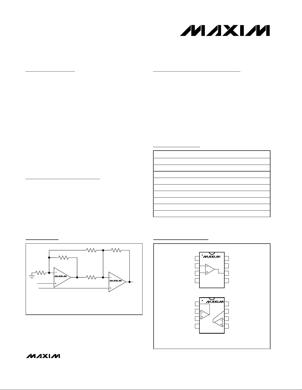
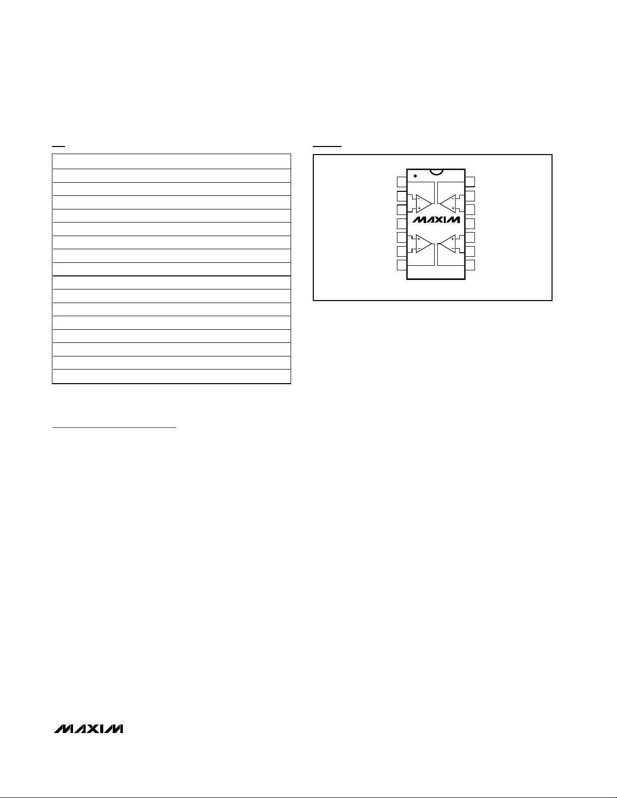
Pin Configurations
+IN
-IN
42.2kΩ**
1%
2
3
200Ω
1%
1
200Ω
1%
1kΩ*
6
5
7
OUT
42.2kΩ
1%
1/2 MAX412
1/2 MAX412
*TRIM FOR GAIN.
**TRIM FOR COMMON-MODE REJECTION.
LOW-NOISE INSTRUMENTATION AMPLIFIER
Typical Operating Circuit
19-4194; Rev 4; 6/03
For pricing, delivery, and ordering information, please contact Maxim/Dallas Direct! at
1-888-629-4642, or visit Maxim’s website at www.maxim-ic.com.
Ordering Information
Ordering Information continued at end of data sheet.
*EP—Exposed paddle. Top Mark—AGQ.
Pin Configurations continued at end of data sheet.
PART TEMP RANGE PIN-PACKAGE
MAX410CPA 0°C to +70°C 8 Plastic DIP
MAX410BCPA 0°C to +70°C 8 Plastic DIP
MAX410CSA 0°C to +70°C 8 SO
MAX410BCSA 0°C to +70°C 8 SO
MAX410EPA -40°C to +85°C 8 Plastic DIP
MAX410BEPA -40°C to +85°C 8 Plastic DIP
MAX410ESA -40°C to +85°C 8 SO
MAX410BESA -40°C to +85°C 8 SO
MAX410ETA -40°C to +85°C 8 TDFN-EP*
TOP VIEW
NULL
IN+
OUT1
IN1+
1
MAX410
2
3
4
DIP/SO/TDFN
1
2
3
4
DIP/SO
MAX412
87NULL
V+IN-
OUT
6
N.C.V-
5
87V+
OUT2IN1-
IN2-
6
IN2+V-
5
Page 2
MAX410/MAX412/MAX414
Single/Dual/Quad, 28MHz, Low-Noise,
Low-Voltage, Precision Op Amps
2 _______________________________________________________________________________________
ABSOLUTE MAXIMUM RATINGS
Stresses beyond those listed under “Absolute Maximum Ratings” may cause permanent damage to the device. These are stress ratings only, and functional
operation of the device at these or any other conditions beyond those indicated in the operational sections of the specifications is not implied. Exposure to
absolute maximum rating conditions for extended periods may affect device reliability.
Supply Voltage .......................................................................12V
Differential Input Current (Note 1) ....................................±20mA
Input Voltage Range........................................................V+ to V-
Common-Mode Input Voltage ..............(V+ + 0.3V) to (V- - 0.3V)
Short-Circuit Current Duration....................................Continuous
Continuous Power Dissipation (T
A
= +70°C)
MAX410/MAX412
8-Pin Plastic DIP (derate 9.09mW/°C above +70°C) ...727mW
8-Pin SO (derate 5.88mW/°C above +70°C)................471mW
8-Pin TDFN (derate 24.4mW/°C above +70°C) .........1951mW
MAX414
14-Pin Plastic DIP (derate 10.00mW/°C above +70°C)800mW
14-Pin SO (derate 8.33mW/°C above +70°C)..............667mW
Operating Temperature Ranges:
MAX41_C_ _ .......................................................0°C to +70°C
MAX41_E_ _.....................................................-40°C to +85°C
Storage Temperature Range .............................-65°C to +150°C
Lead Temperature (soldering, 10s) .................................+300°C
ELECTRICAL CHARACTERISTICS
(V+ = 5V, V- = -5V, TA= +25°C, unless otherwise noted.)
)
Note 1: The amplifier inputs are connected by internal back-to-back clamp diodes. In order to minimize noise in the input stage, current-
limiting resistors are not used. If differential input voltages exceeding ±1.0V are applied, limit input current to 20mA.
Input Offset Voltage V
Input Bias Current I
Input Offset Current I
Differential Input Resistance R
Common-Mode Input Resistance R
Input Capacitance C
Input Noise-Voltage Density e
Input Noise-Current Density i
Common-Mode Input Voltage V
Common-Mode Rejection Ratio CMRR VCM = ±3.5V 115 130 dB
Power-Supply Rejection Ratio PSRR VS = ±2.4V to ±5.25V 96 103 dB
Large-Signal Gain A
Output Voltage Swing V
Short-Circuit Output Current I
Slew Rate SR 10kΩ || 20pF load 4.5 V/µs
Unity-Gain Bandwidth GBW 10kΩ || 20pF load 28 MHz
Settling Time t
Channel Separation C
PARAMETER SYMBOL CONDITIONS MIN TYP MAX UNITS
OS
OS
IN(Diff)
IN(CM
CM
VOL
OUT
SC
MAX410, MAX410B, MAX412, MAX412B ±120 ±250
MAX414, MAX414B ±150 ±320
B
IN
MAX410, MAX412,
MAX414
n
MAX410B, MAX412B,
MAX414B
fO = 10Hz 2.6
n
fO = 1000Hz 1.2
RL = 2kΩ, VO = ±3.6V 115 122
RL = 600Ω, VO = ±3.5V 110 120
RL = 2kΩ
To 0.1% 1.3 µs
S
fO = 1kHz 135 dB
S
±80 ±150 nA
±40 ±80 nA
20 kΩ
40 MΩ
4pF
10Hz 7
1000Hz (Note 2) 1.5 2.4
1000Hz (Note 2) 2.4 4.0
±3.5
+3.6
-3.7
+3.7/
-3.8
+3.7/
-3.8
35 mA
µV
nV√Hz
pA√Hz
V
dB
V
Page 3
MAX410/MAX412/MAX414
Single/Dual/Quad, 28MHz, Low-Noise,
Low-Voltage, Precision Op Amps
_______________________________________________________________________________________ 3
Note 2: Guaranteed by design.
Note 3: All TDFN devices are 100% tested at T
A
= +25°C. Limits over temperature for thin TDFNs are guaranteed by design.
ELECTRICAL CHARACTERISTICS
(V+ = 5V, V- = -5V, TA= 0°C to +70°C, unless otherwise noted.)
ELECTRICAL CHARACTERISTICS
(V+ = 5V, V- = -5V, TA= -40°C to +85°C, unless otherwise noted.) (Note 3)
ELECTRICAL CHARACTERISTICS (continued)
(V+ = 5V, V- = -5V, TA= +25°C, unless otherwise noted.)
Operating Supply-Voltage Range V
Supply Current I
PARAMETER SYMBOL CONDITIONS MIN TYP MAX UNITS
S
Per amplifier 2.5 2.7 mA
S
±2.4 ±5.25 V
Input Offset Voltage V
Offset Voltage Tempco ∆VOS/∆T Over operating temperature range ±1 µV/°C
Input Bias Current I
Input Offset Current I
Common-Mode Input Voltage V
Common-Mode Rejection Ratio CMRR VCM = ±3.5V 105 121 dB
Power-Supply Rejection Ratio PSRR VS = ±2.4V to ±5.25V 90 97 dB
Large-Signal Gain A
Output Voltage Swing V
Supply Current I
PARAMETER SYMBOL CONDITIONS MIN TYP MAX UNITS
OS
B
OS
CM
VOL
OUT
S
±3.5
RL = 2kΩ, VO = ±3.6V 110 120
RL = 600Ω, VO = ±3.5V 90 119
RL = 2kΩ ±3.5
Per amplifier 3.3 mA
±150 ±350 µV
±100 ±200 nA
±80 ±150 nA
+3.7/
-3.8
dB
+3.7/
-3.6
V
V
Input Offset Voltage V
Offset Voltage Tempco ∆VOS/∆T Over operating temperature range ±1 µV/°C
Input Bias Current I
Input Offset Current I
Common-Mode Input Voltage V
Common-Mode Rejection Ratio CMRR VCM = ±3.5V 105 120 dB
Power-Supply Rejection Ratio PSRR VS = ±2.4V to ±5.25V 90 94 dB
Large-Signal Gain A
Output Voltage Swing V
Supply Current I
PARAMETER SYMBOL CONDITIONS MIN TYP MAX UNITS
OS
OS
CM
VOL
OUT
MAX410, MAX410B, MAX412, MAX412B ±200 ±400
MAX414, MAX414B ±200 ±450
B
±3.5
RL = 2kΩ, VO = ±3.6V 110 118
RL = 600Ω, VO = +3.4V to -3.5V 90 114
RL = 2kΩ ±3.5
Per amplifier 3.3 mA
S
±130 ±350 nA
±100 ±200 nA
+3.7/
-3.6
+3.7/
-3.6
µV
V
dB
V
Page 4
MAX410/MAX412/MAX414
Single/Dual/Quad, 28MHz, Low-Noise,
Low-Voltage, Precision Op Amps
4 _______________________________________________________________________________________
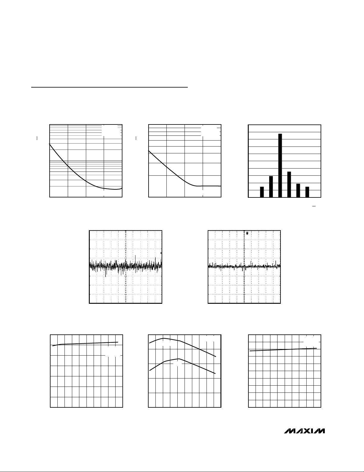
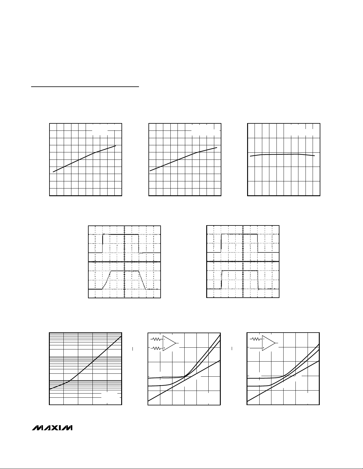
Typical Operating Characteristics
(V+ = 5V, V- = -5V, TA= +25°C, unless otherwise noted.)
1 10k10 100 1k
VOLTAGE-NOISE DENSITY
vs. FREQUENCY
MAX410-14 toc01
FREQUENCY (Hz)
1
10
100
VOLTAGE-NOISE DENSITY (nV/√Hz)
VS = ±5V
T
A
= +25°C
1/F CORNER = 90Hz
1 10k10 100 1k
CURRENT-NOISE DENSITY
vs. FREQUENCY
MAX410-14 toc02
FREQUENCY (Hz)
1
10
CURRENT-NOISE DENSITY (pA/√Hz)
VS = ±5V
T
A
= +25°C
1/F CORNER = 220Hz
0
10
5
20
15
30
25
35
45
40
50
1.3 1.4 1.51.2 1.6 1.7 1.8 1.9
1kHz VOLTAGE NOISE DISTRIBUTION
MAX410-14 toc03
UNITS (%)
INPUT-REFERRED VOLTAGE NOISE (nV/√Hz)
0.1Hz TO 10Hz VOLTAGE NOISE
MAX410-14 toc04
1s/div
100nV/div
(INPUT-REFERRED)
WIDEBAND NOISE DC TO 20kHz
MAX410-14 toc05
0.2ms/div
2µV/div
(INPUT-REFERRED)
0
40
20
80
60
120
100
140
-60 20-20 60 100 140
OPEN-LOOP GAIN
vs. TEMPERATURE
MAX410-14 toc06
TEMPERATURE (°C)
OPEN-LOOP GAIN (dB)
VS = ±5V
R
L
= 2k
Ω
0
10
20
40
30
50
-60 20-20 60 100 140
SHORT-CIRCUIT OUTPUT CURRENT
vs. TEMPERATURE
MAX410-14 toc07
TEMPERATURE (°C)
SHORT-CIRCUIT OUTPUT CURRENT (mA)
VS = ±5V
SOURCE
SINK
0
10
9
8
7
6
5
4
3
2
1
-60 20-20 60 100 140
OUTPUT VOLTAGE SWING
vs. TEMPERATURE
MAX410-14 toc08
TEMPERATURE (°C)
OUTPUT VOLTAGE SWING (V
P-P
)
VS = ±5V
R
L
= 2k
Ω
Page 5
MAX410/MAX412/MAX414
Single/Dual/Quad, 28MHz, Low-Noise,
Low-Voltage, Precision Op Amps
_______________________________________________________________________________________ 5
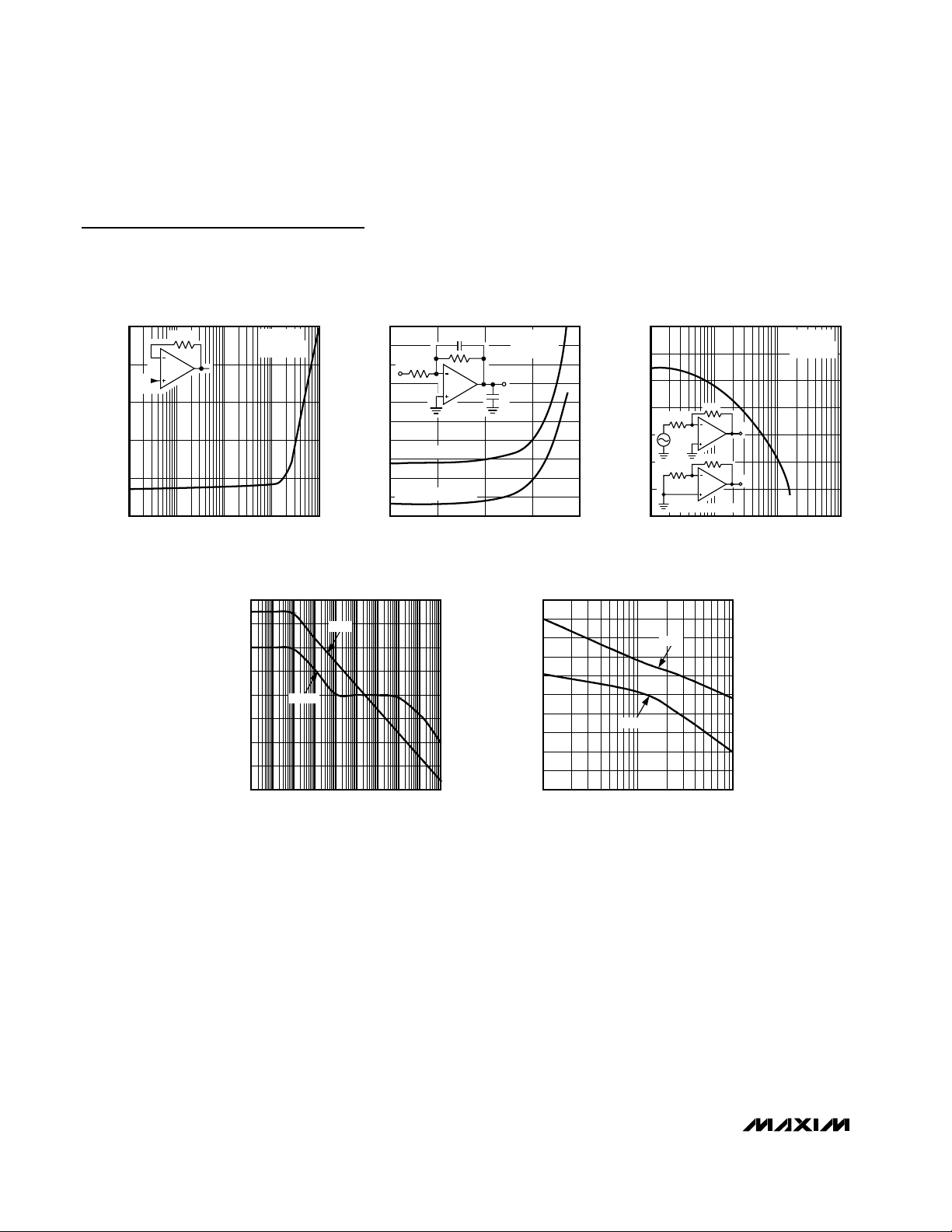
Typical Operating Characteristics (continued)
(V+ = 5V, V- = -5V, TA= +25°C, unless otherwise noted.)
SUPPLY CURRENT
5
4
3
2
SUPPLY CURRENT (mA)
1
0
-60 20-20 60 100 140
vs. TEMPERATURE
EACH AMPLIFIER
= ±5V
V
S
TEMPERATURE (°C)
LARGE-SIGNAL TRANSIENT RESPONSE
INPUT
3V/div
MAX410-14 toc09
10
9
8
7
6
5
4
SLEW RATE (V/µs)
3
2
1
0
-60 20-20 60 100 140
MAX410-14 toc12
SLEW RATE
vs. TEMPERATURE
TEMPERATURE (°C)
GND
VS = ±5V
= 10kΩ II 20pF
R
L
MAX410-14 toc10
UNITY-GAIN BANDWIDTH (MHz)
SMALL-SIGNAL TRANSIENT RESPONSE
INPUT
50mV/div
UNITY-GAIN BANDWIDTH
vs. TEMPERATURE
50
40
30
20
10
0
-60 20-20 60 100 140
TEMPERATURE (°C)
MAX410-14 toc13
GND
VS = ±5V
= 10kΩ II 20pF
R
L
MAX410-14 toc11
OUTPUT
3V/div
= +1, RF = 499Ω, RL = 2kΩ II 20pF, VS = ±5V, TA = +25°C
A
V
WIDEBAND VOLTAGE NOISE
(0.1Hz TO FREQUENCY INDICATED)
10
1
0.1
RMS VOLTAGE NOISE (µV)
0.01
100 1k 10k 100k 1M 10M
BANDWIDTH (Hz)
VS = ±5V
= +25°C
T
A
1µs/div
MAX410-14 toc14
GND
OUTPUT
50mV/div
TOTAL NOISE DENSITY
vs. MATCHED SOURCE RESISTANCE
10k
R
S
R
S
1k
100
@10Hz
10
@1kHz
1
TOTAL NOISE DENSITY (nV/√Hz)
0.1
110010 1k 10k 100k 1M
MATCHED SOURCE RESISTANCE (Ω)
NOISE ONLY
S
R
200ns/div
A
= +1, RF = 499Ω, RL = 2kΩ II 20pF, VS = ±5V, TA = +25°C
V
TOTAL NOISE DENSITY
vs. UNMATCHED SOURCE RESISTANCE
10k
R
S
1k
MAX410-14 toc15
100
@10Hz
10
@1kHz
1
VS = ±5V
= +25°C
T
A
TOTAL NOISE DENSITY (nV/√Hz)
0.1
1 10010 1k 10k 100k 1M
UNMATCHED SOURCE RESISTANCE (Ω)
GND
NOISE ONLY
S
R
VS = ±5V
= +25°C
T
A
MAX410-14 toc16
Page 6
MAX410/MAX412/MAX414
Single/Dual/Quad, 28MHz, Low-Noise,
Low-Voltage, Precision Op Amps
6 _______________________________________________________________________________________
Typical Operating Characteristics (continued)
(V+ = 5V, V- = -5V, TA= +25°C, unless otherwise noted.)
-85
-88
-91
-94
-97
-100
20 100 10k 50k
TOTAL HARMONIC DISTORTION PLUS
NOISE vs. FREQUENCY
MAX410-14 toc17
FREQUENCY (Hz)
THD+N (dB)
1k
VS = ±5V
T
A
= +25°C
499Ω
V
IN
7V
P-P
0
50
45
40
35
30
25
20
15
10
5
1 10 100 1000 10,000
PERCENTAGE OVERSHOOT
vs. CAPACITIVE LOAD
MAX410-14 toc18
CAPACITANCE LOAD (pF)
OVERSHOOT (%)
VS = ±5V
T
A
= +25°C
AV = -1, RS = 2k
Ω
AV = -10, RS = 200
Ω
C
L
R
S
30pF
2kΩ
150
80
1 100 1000
MAX412/MAX414
CHANNEL SEPARATION vs. FREQUENCY
100
90
140
130
120
110
MAX410-14 toc19
FREQUENCY (kHz)
CHANNEL SEPARATION (dB)
10
VS = ±5V
T
A
= +25°C
500Ω
V
01
CHANNEL SEPARATION = 20 log
IN
500Ω
10Ω
V
02
1kΩ
GAIN AND PHASE vs. FREQUENCY
FREQUENCY (kHz)
VOLTAGE GAIN (dB)
140
-20
120
100
80
60
40
20
0
90
-270
45
0
-45
-90
-135
-180
-225
0.001
0.0001 0.01
0.1
1
10
100
1,000
10,000
100,000
MAX410-14 toc20
GAIN
PHASE
PHASE (DEGREES)
40
30
20
10
0
-10
-20
-30
-40
-50
-60
0
-45
-90
-135
-180
-225
1 10 100
GAIN AND PHASE vs. FREQUENCY
FREQUENCY (MHz)
VOLTAGE GAIN (dB)
MAX410-14 toc21
GAIN
PHASE
PHASE (DEGREES)
Page 7
Applications Information
The MAX410/MAX412/MAX414 provide low voltagenoise performance. Obtaining low voltage noise from a
bipolar op amp requires high collector currents in the
input stage, since voltage noise is inversely proportional to the square root of the input stage collector current.
However, op amp current noise is proportional to the
square root of the input stage collector current, and the
input bias current is proportional to the input stage collector current. Therefore, to obtain optimum low-noise
performance, DC accuracy, and AC stability, minimize
the value of the feedback and source resistance.
Total Noise Density vs. Source Resistance
The standard expression for the total input-referred
noise of an op amp at a given frequency is:
where:
Rn= Inverting input effective series resistance
Rp = Noninverting input effective series resistance
en= Input voltage-noise density at the frequency of
interest
in= Input current-noise density at the frequency of
interest
T = Ambient temperature in Kelvin (K)
k = 1.28 x 10
-23
J/K (Boltzman’s constant)
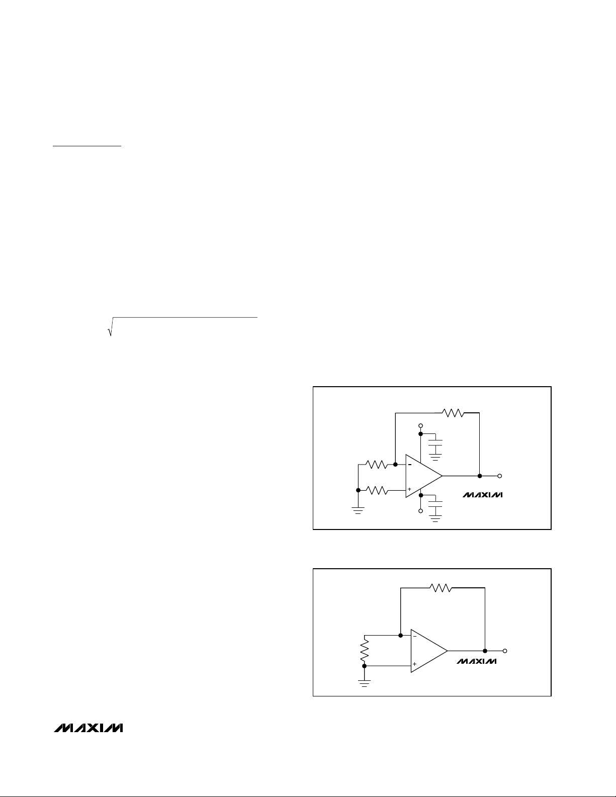
In Figure 1, R
p
= R3 and Rn= R1 || R2. In a real application, the output resistance of the source driving the
input must be included with R
p
and Rn. The following
example demonstrates how to calculate the total output-noise density at a frequency of 1kHz for the
MAX412 circuit in Figure 1.
Gain = 1000
4kT at +25°C = 1.64 x 10
-20
Rp= 100Ω
Rn= 100Ω || 100kΩ = 99.9 W
en= 1.5nV/√Hz at 1kHz
in= 1.2pA/√Hz at 1kHz
et= [(1.5 x 10⁻⁹)2+ (100 + 99.9)2(1.2 x 10
-12)2
+ (1.64
x 10
-20
) (100 + 99.9)]
1/2
= 2.36nV/√Hz at 1kHz
Output noise density = (100)et= 2.36µV/√Hz at 1kHz.
In general, the amplifier’s voltage noise dominates with
equivalent source resistances less than 200Ω. As the
equivalent source resistance increases, resistor noise
becomes the dominant term, eventually making the
voltage noise contribution from the MAX410/MAX412/
MAX414 negligible. As the source resistance is further
increased, current noise becomes dominant. For example, when the equivalent source resistance is greater
than 3kΩ at 1kHz, the current noise component is larger than the resistor noise. The graph of Total Noise
Density vs. Matched Source Resistance in the Typical
Operating Characteristics shows this phenomenon.
Optimal MAX410/MAX412/MAX414 noise performance
and minimal total noise achieved with an equivalent
source resistance of less than 10kΩ.
Voltage Noise Testing
RMS voltage-noise density is measured with the circuit
shown in Figure 2, using the Quan Tech model 5173
noise analyzer, or equivalent. The voltage-noise density
at 1kHz is sample tested on production units. When
measuring op-amp voltage noise, only low-value, metal
film resistors are used in the test fixture.
The 0.1Hz to 10Hz peak-to-peak noise of the
MAX410/MAX412/MAX414 is measured using the test
MAX410/MAX412/MAX414
Single/Dual/Quad, 28MHz, Low-Noise,
Low-Voltage, Precision Op Amps
_______________________________________________________________________________________ 7
Figure 1. Total Noise vs. Source Resistance Example
Figure 2. Voltage-Noise Density Test Circuit
ee i
2
tnpnn pn
+(R +R ) + 4kT (R + R )=
2
2
R2
100kΩ
+5V
D.U.T
27Ω
0.1µF
0.1µF
MAX410
MAX412
MAX414
MAX410
MAX412
MAX414
e
t
e
n
R1
100Ω
D.U.T
R3
100Ω
3Ω
-5V
Page 8

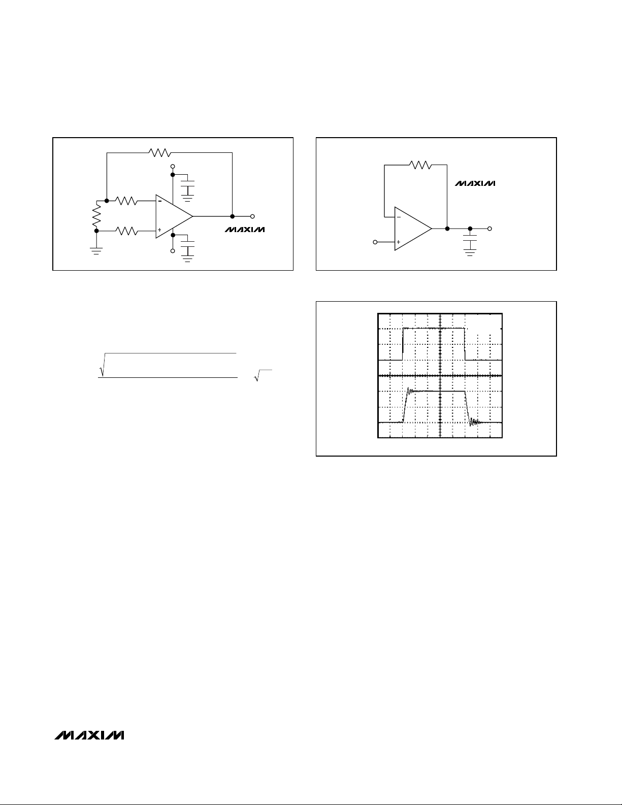
MAX410/MAX412/MAX414
circuit shown in Figure 3. Figure 4 shows the frequency
response of the circuit. The test time for the 0.1Hz to
10Hz noise measurement should be limited to 10 seconds, which has the effect of adding a second zero to
the test circuit, providing increased attenuation for frequencies below 0.1Hz.
Current Noise Testing
The current-noise density can be calculated, once the
value of the input-referred noise is determined, by
using the standard expression given below:
where:
Rn= Inverting input effective series resistance
Rp= Noninverting input effective series resistance
eno= Output voltage-noise density at the frequency of
interest (V/√Hz)
in= Input current-noise density at the frequency of
interest (A/√Hz)
A
VCL
= Closed-loop gain
T = Ambient temperature in Kelvin (K)
k = 1.38 x 10
-23
J/K (Boltzman’s constant)
Rpand Rninclude the resistances of the input driving
source(s), if any.
If the Quan Tech model 5173 is used, then the A
VCL
terms in the numerator and denominator of the equation
given above should be eliminated because the Quan
Single/Dual/Quad, 28MHz, Low-Noise,
Low-Voltage, Precision Op Amps
8 _______________________________________________________________________________________
Figure 3. 0.1Hz to 10Hz Voltage Noise Test Circuit
Figure 4. 0.1Hz to 10Hz Voltage Noise Test Circuit, Frequency
Response
FREQUENCY (Hz)
GAIN (dB)
1010.1
20
40
60
80
100
0
0.01 100
0.1µF
100kΩ
+V
S
10Ω D.U.T
-V
S
MAX410
MAX412
MAX414
2kΩ
4.7µF
24.9kΩ
+V
MAX410
100kΩ
0.1µF
S
-V
S
2kΩ
4.7µF
22µF
TO SCOPE x1
R
= 1MΩ
IN
110kΩ
i
=
n
2
e
- (A ) (4kT)(R +R )
no VCL n p
[]
(R +R )(A )
2
n p VCL
AHz
/
Page 9
Tech measures input-referred noise. For the circuit in
Figure 5, assuming Rpis approximately equal to R
n
and the measurement is taken with the Quan Tech
model 5173, the equation simplifies to:
Input Protection
To protect amplifier inputs from excessive differential
input voltages, most modern op amps contain input
protection diodes and current-limiting resistors. These
resistors increase the amplifier’s input-referred noise.
They have not been included in the MAX410/MAX412/
MAX414, to optimize noise performance. The MAX410/
MAX412/MAX414 do contain back-to-back input protection diodes which will protect the amplifier for differential input voltages of ±0.1V. If the amplifier must be
protected from higher differential input voltages, add
external current-limiting resistors in series with the op
amp inputs to limit the potential input current to less
than 20mA.
Capacitive-Load Driving
Driving large capacitive loads increases the likelihood
of oscillation in amplifier circuits. This is especially true
for circuits with high loop gains, like voltage followers.
The output impedance of the amplifier and a capacitive
load form an RC network that adds a pole to the loop
response. If the pole frequency is low enough, as when
driving a large capacitive load, the circuit phase margin is degraded.
In voltage follower circuits, the MAX410/MAX412/
MAX414 remain stable while driving capacitive loads
as great as 3900pF (see Figures 6a and 6b).
When driving capacitive loads greater than 3900pF,
add an output isolation resistor to the voltage follower
circuit, as shown in Figure 7a. This resistor isolates the
load capacitance from the amplifier output and restores
the phase margin. Figure 7b is a photograph of the
response of a MAX410/MAX412/MAX414 driving a
0.015µF load with a 10Ω isolation resistor
The capacitive-load driving performance of the
MAX410/MAX412/MAX414 is plotted for closed-loop
gains of -1V/V and -10V/V in the % Overshoot vs.
Capacitive Load graph in the Typical Operating
Characteristics.
Feedback around the isolation resistor RI increases the
accuracy at the capacitively loaded output (see Figure 8).
The MAX410/MAX412/MAX414 are stable with a 0.01µF
load for the values of RIand CFshown. In general, for
decreased closed-loop gain, increase RIor CF. To drive
larger capacitive loads, increase the value of CF.
MAX410/MAX412/MAX414
Single/Dual/Quad, 28MHz, Low-Noise,
Low-Voltage, Precision Op Amps
_______________________________________________________________________________________ 9
Figure 5. Current-Noise Test Circuit
100Ω
Figure 6a. Voltage Follower Circuit with 3900pF Load
Figure 6b. Driving 3900pF Load as Shown in Figure 6a
R
10kΩ
R
10kΩ
909Ω
+5V
n
D.U.T
p
-5V
0.022µF
0.022µF
MAX410
MAX412
MAX414
e
no
V
IN
D.U.T
R
499Ω
f
MAX410
MAX412
MAX414
V
OUT
3900pF
i
=
n
2
e
- (1.64 10 )(20 10 )
no
[]
-20 3
××
3
×
(20 10 )
/
AHz
VS = ±5V
= +25°C
T
INPUT
1V/div
OUTPUT
1V/div
1µs/div
A
GND
GND
Page 10

MAX410/MAX412/MAX414
TDFN Exposed Paddle Connection
On TDFN packages, there is an exposed paddle that
does not carry any current but should be connected to
V- (not the GND plane) for rated power dissipation.
Total Supply Voltage Considerations
Although the MAX410/MAX412/MAX414 are specified
with ±5V power supplies, they are also capable of single-supply operation with voltages as low as 4.8V. The
minimum input voltage range for normal amplifier operation is between V- + 1.5V and V+ - 1.5V. The minimum
room-temperature output voltage range (with 2kΩ load)
is between V+ - 1.4V and V- + 1.3V for total supply voltages between 4.8V and 10V. The output voltage range,
referenced to the supply voltages, decreases slightly
over temperature, as indicated in the ±5V Electrical
Characteristics tables. Operating characteristics at total
supply, voltages of less than 10V are guaranteed by
design and PSRR tests.
MAX410 Offset Voltage Null
The offset null circuit of Figure 9 provides approximately
±450µV of offset adjustment range, sufficient for zeroing
offset over the full operating temperature range,
Single/Dual/Quad, 28MHz, Low-Noise,
Low-Voltage, Precision Op Amps
10 ______________________________________________________________________________________
Figure 7b. Driving a 0.015µF Load with a 10ΩIsolation Resistor
Figure 7a. Capacitive-Load Driving Circuit
Figure 8. Capacitive-Load Driving Circuit with Loop-Enclosed
Isolation Resistor
Figure 9. MAX410 Offset Null Circuit
10kΩ
499Ω
C
MAX410
MAX412
MAX414
R
I
D.U.T
V
IN
10Ω
V
OUT
CL > 0.015µF
1kΩ
V
IN
909Ω
82pF
D.U.T
F
MAX410
MAX412
MAX414
R
10Ω
I
V
OUT
C
L
0.01µF
VS = ±5V
= +25°C
T
A
INPUT
1V/div
OUTPUT
1V/div
1µs/div
GND
GND
10kΩ
1
NULL
NULL
8
MAX410
7
V+
Page 11
Chip Information
MAX410 TRANSISTOR COUNT: 132
MAX412 TRANSISTOR COUNT: 262
MAX414 TRANSISTOR COUNT: 2 ✕262 (hybrid)
PROCESS: Bipolar
MAX410/MAX412/MAX414
Single/Dual/Quad, 28MHz, Low-Noise,
Low-Voltage, Precision Op Amps
______________________________________________________________________________________ 11
Ordering Information (continued)
Pin Configurations (continued)
PART TEMP RANGE PIN-PACKAGE
MAX412CPA 0°C to +70°C 8 Plastic DIP
MAX412BCPA 0°C to +70°C 8 Plastic DIP
MAX412CSA 0°C to +70°C 8 SO
MAX412BCSA 0°C to +70°C 8 SO
MAX412EPA -40°C to +85°C 8 Plastic DIP
MAX412BEPA -40°C to +85°C 8 Plastic DIP
MAX412ESA -40°C to +85°C 8 SO
MAX412BESA -40°C to +85°C 8 SO
MAX414CPD 0°C to +70°C 14 Plastic DIP
MAX414BCPD 0°C to +70°C 14 Plastic DIP
MAX414CSD 0°C to +70°C 14 SO
MAX414BCSD 0°C to +70°C 14 SO
MAX414EPD -40°C to +85°C 14 Plastic DIP
MAX414BEPD -40°C to +85°C 14 Plastic DIP
MAX414ESD -40°C to +85°C 14 SO
MAX414BESD -40°C to +85°C 14 SO
TOP VIEW
OUT1
IN1-
IN1+
IN2+
IN2-
1
2
3
4
5
6
7
1
MAX414
2
DIP/SO
4
3
OUT4
14
IN4-
13
IN4+
12
V-V+
11
10
IN3+
9
IN3-
8
OUT3OUT2
Page 12

MAX410/MAX412/MAX414
Single/Dual/Quad, 28MHz, Low-Noise,
Low-Voltage, Precision Op Amps
12 ______________________________________________________________________________________
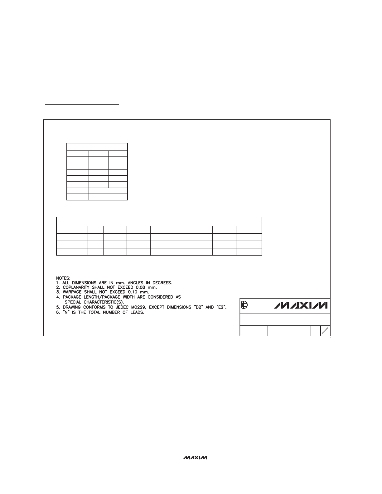
Package Information
(The package drawing(s) in this data sheet may not reflect the most current specifications. For the latest package outline information,
go to www.maxim-ic.com/packages
.)
PDIPN.EPS
Page 13

MAX410/MAX412/MAX414
Single/Dual/Quad, 28MHz, Low-Noise,
Low-Voltage, Precision Op Amps
______________________________________________________________________________________ 13
Package Information (continued)
(The package drawing(s) in this data sheet may not reflect the most current specifications. For the latest package outline information,
go to www.maxim-ic.com/packages
.)
N
1
TOP VIEW
D
e
FRONT VIEW
INCHES
DIM
MIN
0.053A
0.004
A1
0.014
B
0.007
C
e 0.050 BSC 1.27 BSC
0.150
HE
A
B
A1
C
L
E
H 0.2440.228 5.80 6.20
0.016L
VARIATIONS:
INCHES
MINDIM
D
0.189 0.197 AA5.004.80 8
0.337 0.344 AB8.758.55 14
D
0-8
SIDE VIEW
MAX
0.069
0.010
0.019
0.010
0.157
0.050
MAX
0.3940.386D
MILLIMETERS
MAX
MIN
1.35
1.75
0.10
0.25
0.35
0.49
0.19
0.25
3.80 4.00
0.40 1.27
MILLIMETERS
MAX
MIN
9.80 10.00
N MS012
16
AC
SOICN .EPS
PROPRIETARY INFORMATION
TITLE:
PACKAGE OUTLINE, .150" SOIC
REV.DOCUMENT CONTROL NO.APPROVAL
21-0041
1
B
1
Page 14

MAX410/MAX412/MAX414
Single/Dual/Quad, 28MHz, Low-Noise,
Low-Voltage, Precision Op Amps
14 ______________________________________________________________________________________
Package Information (continued)
(The package drawing(s) in this data sheet may not reflect the most current specifications. For the latest package outline information,
go to www.maxim-ic.com/packages
.)
A
A2
A1
PIN 1
INDEX
AREA
D
E
A
NUMBER OF LEADS SHOWN ARE FOR REFERENCE ONLY
DETAIL A
L
L
D2
PIN 1 ID
1N1
b
E2
e
C
L
e
C0.35
k
C
L
L
e
DALLAS
SEMICONDUCTOR
PROPRIETARY INFORMATION
TITLE:
PACKAGE OUTLINE, 6, 8 & 10L,
TDFN, EXPOSED PAD, 3x3x0.80 mm
APPROVAL
DOCUMENT CONTROL NO. REV.
21-0137 D
[(N/2)-1] x e
REF.
6, 8, &10L, QFN THIN.EPS
1
2
Page 15
MAX410/MAX412/MAX414
Single/Dual/Quad, 28MHz, Low-Noise,
Low-Voltage, Precision Op Amps
Maxim cannot assume responsibility for use of any circuitry other than circuitry entirely embodied in a Maxim product. No circuit patent licenses are
implied. Maxim reserves the right to change the circuitry and specifications without notice at any time.
Maxim Integrated Products, 120 San Gabriel Drive, Sunnyvale, CA 94086 408-737-7600 ____________________ 15
© 2003 Maxim Integrated Products Printed USA is a registered trademark of Maxim Integrated Products.
Package Information (continued)
(The package drawing(s) in this data sheet may not reflect the most current specifications. For the latest package outline information,
go to www.maxim-ic.com/packages
.)
COMMON DIMENSIONS
SYMBOL
A
D
E
A1
L
k
A2 0.20 REF.
PACKAGE VARIATIONS
PKG. CODE
T633-1 1.50–0.10D22.30–0.10
MIN. MAX.
0.70 0.80
2.90 3.10
2.90 3.10
0.00 0.05
0.20 0.40
0.25 MIN.
N
6
1.50–0.10
E2
0.95 BSCeMO229 / WEEA
2.30–0.10T833-1 8
0.65 BSC
JEDEC SPEC
MO229 / WEEC
[(N/2)-1] x e
0.40–0.05b1.90 REF
1.95 REF0.30–0.05
0.25–0.05 2.00 REFMO229 / WEED-30.50 BSC1.50–0.10 2.30–0.1010T1033-1
DALLAS
SEMICONDUCTOR
PROPRIETARY INFORMATION
TITLE:
PACKAGE OUTLINE, 6, 8 & 10L,
TDFN, EXPOSED PAD, 3x3x0.80 mm
DOCUMENT CONTROL NO.APPROVAL
21-0137
REV.
2
2
D
 Loading...