

General Description
The MAX4090 3V/5V, 6dB video buffer with sync-tip
clamp, and low-power shutdown mode is available in
tiny SOT23, SC70, and µDFN packages. The MAX4090
is designed to drive DC-coupled, 150Ω back-terminated
video loads in portable video applications such as digital still cams, portable DVD players, digital camcorders,
PDAs, video-enabled cell phones, portable game systems, and notebook computers. The input clamp positions the video waveform at the output and allows the
MAX4090 to be used as a DC-coupled output driver.
The MAX4090 operates from a single 2.7V to 5.5V supply and consumes only 6.5mA of supply current. The
low-power shutdown mode reduces the supply current
to 150nA, making the MAX4090 ideal for low-voltage,
battery-powered video applications.
The MAX4090 is available in tiny 6-pin SOT23, SC70,
and µDFN packages and is specified over the extended (-40°C to +85°C) and automotive (-40°C to +125°C)
temperature ranges.
Applications
Portable Video/Game Systems/DVD Players
Digital Camcorders/Televisions/Still Cameras
PDAs
Video-Enabled Cell Phones
Notebook Computers
Portable/Flat-Panel Displays
Features
♦ Single-Supply Operation from 2.7V to 5.5V
♦ Input Sync-Tip Clamp
♦ DC-Coupled Output
♦ Low-Power Shutdown Mode Reduces Supply
Current to 150nA
♦ Available in Space-Saving SOT23, SC70, and
µDFN Packages
MAX4090
3V/5V, 6dB Video Buffer with Sync-Tip Clamp
and 150nA Shutdown Current
________________________________________________________________ Maxim Integrated Products 1
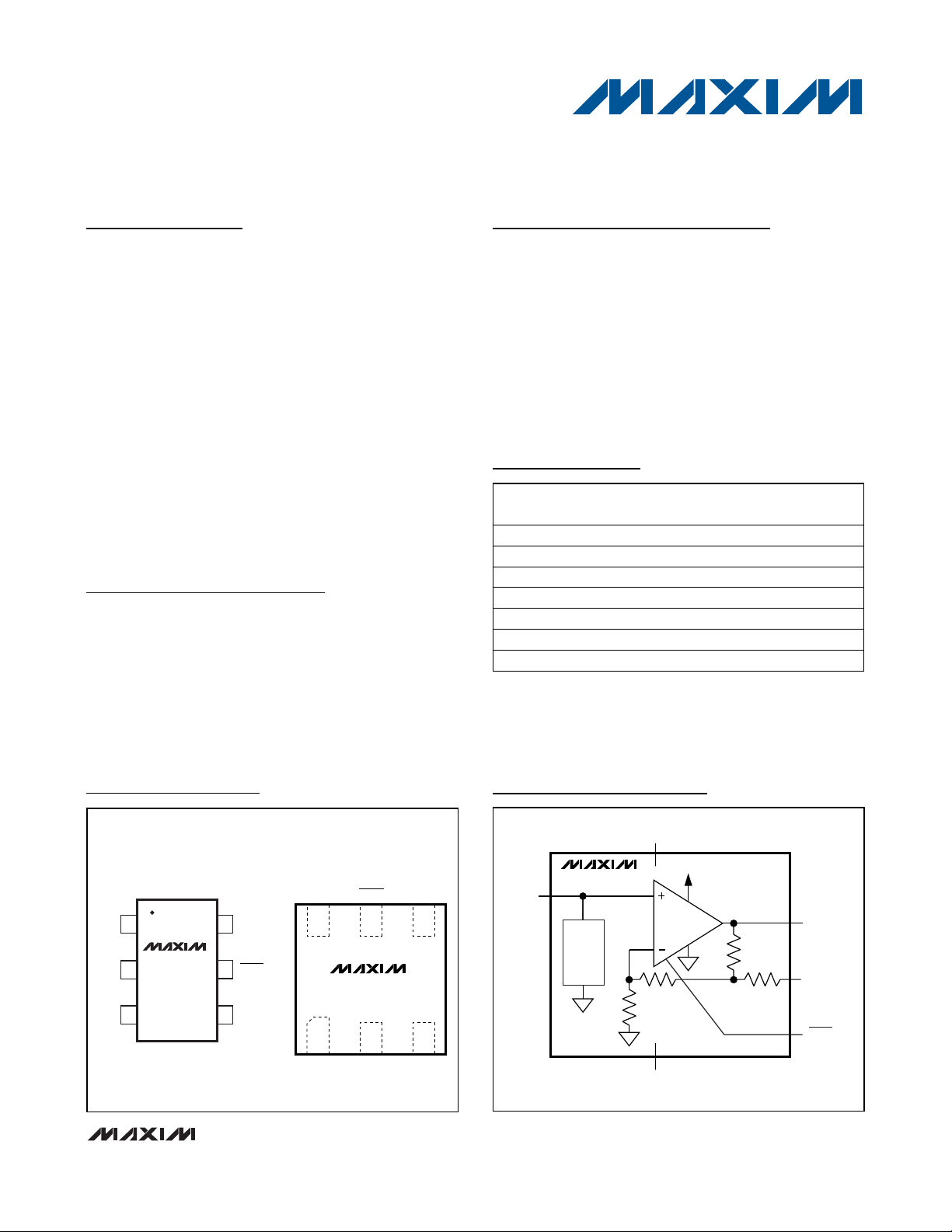
Ordering Information
GND
V
CC
IN
16FB
5 SHDN
OUT
MAX4090
SC70/SOT23
2
34
123
654
FB OUTSHDN
V
CC
INGND
MAX4090
μDFN
TOP VIEW
Pin Configurations
19-2813; Rev 4; 11/09
For pricing, delivery, and ordering information, please contact Maxim Direct at 1-888-629-4642,
or visit Maxim’s website at www.maxim-ic.com.
MAX4090
CLAMP
1.2kΩ
2.3kΩ
580Ω
780Ω
IN
OUT
FB
SHDN
GND
V
CC
Block Diagram
/V denotes an automotive qualified part.
PART TEMP RANGE
MAX4090EXT-T -40°C to +85°C 6 SC70 ABM
MAX4090EUT-T -40°C to +85°C 6 SOT23 ABOX
MAX4090EUT/V+T -40°C to +85°C 6 SOT23 ABOX
MAX4090ELT-T -40°C to +85°C 6 µDFN AAI
MAX4090AAXT-T -40°C to +125°C 6 SC70 ACW
MAX4090AAUT-T -40°C to +125°C 6 SOT23 ABWQ
MAX4090AALT-T -40°C to +125°C 6 µDFN AAN
PINPACKAGE
TOP
MARK
MAX4090
3V/5V, 6dB Video Buffer with Sync-Tip Clamp
and 150nA Shutdown Current
2 _______________________________________________________________________________________
ABSOLUTE MAXIMUM RATINGS
DC ELECTRICAL CHARACTERISTICS
(VCC= 3.0V, V
GND
= 0V, C
IN
= 0.1µF from IN to GND, RL= infinity to GND, FB shorted to OUT, V
SHDN
= 3.0V, TA= -40°C to +85°C
(MAX4090E), T
A
= -40°C to +125°C (MAX4090A). Typical values are at TA= +25°C, unless otherwise noted.) (Note 2)
Stresses beyond those listed under “Absolute Maximum Ratings” may cause permanent damage to the device. These are stress ratings only, and functional
operation of the device at these or any other conditions beyond those indicated in the operational sections of the specifications is not implied. Exposure to
absolute maximum rating conditions for extended periods may affect device reliability.
Note 1: V
CLP
is the input clamp voltage as defined in the DC Electrical Characteristics table.
V
CC
to GND............................................................. -0.3V to +6V
OUT, FB, SHDN to GND............................ -0.3V to (V
CC
+ 0.3V)
IN to GND (Note 1) ................................... V
CLP
to (VCC+ 0.3V)
IN Short-Circuit Duration from -0.3V to V
CLP
........................1min
Output Short-Circuit Duration to V
CC
or GND .......... Continuous
Continuous Power Dissipation (T
A
= +70°C)
6-Pin SOT23 (derate 8.7mW/°C above +70°C) ...........695mW
6-Pin SC70 (derate 3.1mW/°C above +70°C) .............245mW
6-Pin µDFN (derate 3.6mW/°C above +70°C) ..............290mW
Operating Temperature Range
MAX4090E .......................................................-40°C to +85°C
MAX4090A.....................................................-40°C to +125°C
Junction Temperature .....................................................+150°C
Storage Temperature Range ............................-65°C to +150°C
Lead Temperature (soldering, 10s) ................................+300°C
(
)
PARAMETER SYMBOL CONDITIONS MIN TYP MAX UNITS
Supply Voltage Range V
Quiescent Supply Current I
Shutdown Supply Current I
Input Clamp Voltage V
Input Voltage Range V
Input Bias Current I
Input Resistance V
Voltage Gain A
Power-Supply Rejection Ratio PSRR 2.7V < VCC < 5.5V 60 80 dB
Output-Voltage High Swing V
Output-Voltage Low Swing V
Output Current I
Output Short-Circuit Current I
SHDN Logic-Low Threshold V
SHDN Logic-High Threshold V
SHDN Input Current I
Shutdown Output Impedance
CC
CC
SHDN
CLP
BIAS
OH
OL
OUT
SC
IH
R
OUT
Disabled
Guaranteed by PSRR 2.7 5.5 V
VIN = V
CLP
V
= 0V 0.15 1 µA
SHDN
Input referred 0.27 0.38 0.47 V
Inferred from voltage gain (Note 3) V
IN
VIN = 1.45V 22.5 35 µA
+ 0.5V < VIN < V
CLP
RL = 150Ω, 0.5V < VIN < 1.45V (Note 4) 1.9 2 2.1 V/V
V
RL = 150Ω to GND
RL = 150Ω to GND V
Sourcing, RL = 20Ω to GND 45 85
Sinking, RL = 20Ω to V
OUT shorted to VCC or GND 110 mA
IL
IH
V
= 0V
SHDN
VCC = 3V 6.5 10
VCC = 5V 6.5 10
CLP
+ 1V 3 MΩ
CLP
1.45 V
VCC = 3V 2.55 2.7
V
= 5V 4.3 4.6
CC
0.47 V
CC
CLP
40 85
VCC x 0.3 V
VCC x 0.7 V
0.003 1 µA
At DC 4
At 3.58MHz or
4.43MHz
2
mA
V
mA
kΩ
MAX4090
3V/5V, 6dB Video Buffer with Sync-Tip Clamp
and 150nA Shutdown Current
_______________________________________________________________________________________ 3
Note 2: All devices are 100% production tested at TA= +25°C. Specifications over temperature limits are guaranteed by design.
Note 3: Voltage gain (A
V
) is referenced to the clamp voltage, i.e., an input voltage of VIN= V
CLP
+ VI would produce an output volt-
age of V
OUT
= V
CLP
+ AVx VI.
Note 4: Droop is guaranteed by the Input Bias Current specification.
AC ELECTRICAL CHARACTERISTICS
(VCC= 3.0V, V
GND
= 0V, FB shorted to OUT, CIN= 0.1µF, RIN= 75Ω to GND, RL= 150Ω to GND, V
SHDN
= VCC, TA= +25°C, unless
otherwise noted.)
PARAMETER SYMBOL CONDITIONS MIN TYP MAX UNITS
Small-Signal -3dB Bandwidth BW
Large-Signal -3dB Bandwidth BW
Small-Signal 0.1dB Gain Flatness BW
Large-Signal 0.1dB Gain Flatness BW
Slew Rate SR V
Settling Time to 0.1% t
Power-Supply Rejection Ratio PSRR f = 100kHz 50 dB
Output Impedance Z
Differential Gain DG NTSC
Differential Phase DP NTSC
Group Delay D/dT f = 3.58MHz or 4.43MHz 20 ns
Peak Signal to RMS Noise SNR VIN = 1V
Droop CIN = 0.1µF (Note 4) 2 3 %
SHDN Enable Time t
SHDN Disable Time t
V
SS
LS
0.1dBSSVOUT
0.1dBLSVOUT
S
OUT
ON
OFF
= 100mV
OUT
V
= 2V
OUT
= 100mV
= 2V
= 2V step 275 V/µs
OUT
V
= 2V step 25 ns
OUT
f = 5MHz 2.5 Ω
VIN = V
settled to within 1% of the final voltage
VIN = V
settled to below 1% of the output voltage
P-P
P-P
P-P
P-P
VCC = 3V 1
= 5V 0.5
V
CC
VCC = 3V 0.8
= 5V 0.5
V
CC
, 10MHz BW 65 dB
P-P
CLP
CLP
+ 1V, V
+ 1V, V
SHDN
SHDN
= 3V, V
= 0V, V
OUT
OUT
55 MHz
45 MHz
25 MHz
17 MHz
250 ns
50 ns
Degrees
%
MAX4090
3V/5V, 6dB Video Buffer with Sync-Tip Clamp
and 150nA Shutdown Current
4 _______________________________________________________________________________________
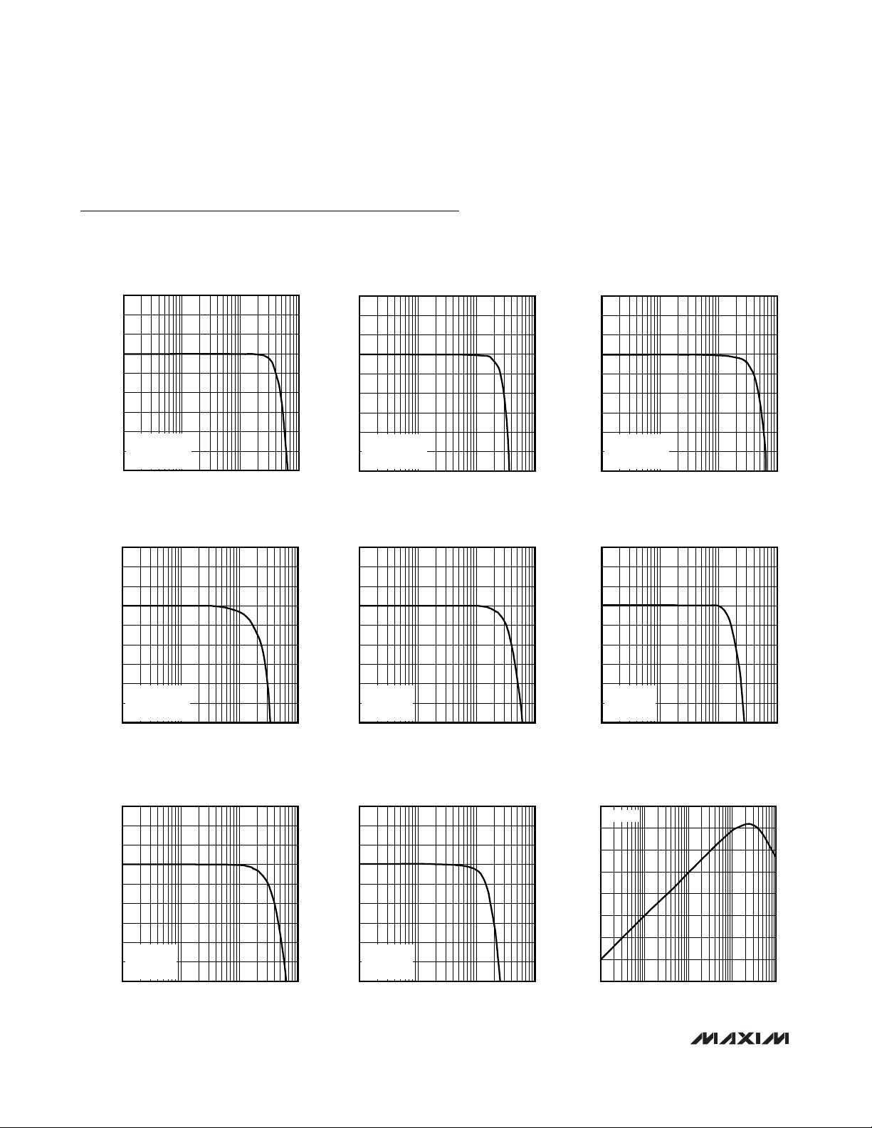
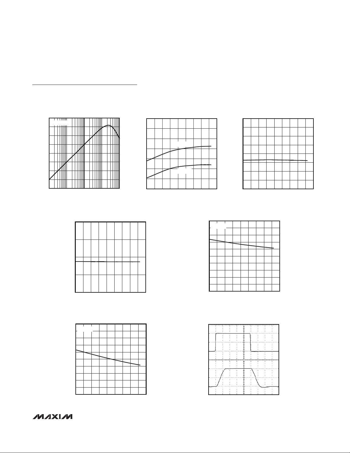
Typical Operating Characteristics
(VCC= 3.0V, GND = 0V, FB shorted to OUT, CIN= 0.1µF, RIN= 75Ω to GND, RL= 150Ω to GND, SHDN = VCC, TA= +25°C, unless
otherwise noted.)
SMALL-SIGNAL GAIN
vs. FREQUENCY
MAX4090 toc01
FREQUENCY (Hz)
GAIN (dB)
10M1M
-5
-4
-3
-2
-1
0
1
2
3
-6
100k 100M
AV = 2
V
CC
= 3V
V
OUT
= 100mV
P-P
SMALL-SIGNAL GAIN FLATNESS
vs. FREQUENCY
MAX4090 toc02
FREQUENCY (Hz)
GAIN (dB)
10M1M
-0.5
-0.4
-0.3
-0.2
-0.1
0
0.1
0.2
0.3
-0.6
100k 100M
AV = 2
V
CC
= 3V
V
OUT
= 100mV
P-P
SMALL-SIGNAL GAIN
vs. FREQUENCY
MAX4090 toc03
FREQUENCY (Hz)
GAIN (dB)
10M1M
-5
-4
-3
-2
-1
0
1
2
3
-6
100k 100M
AV = 2
V
CC
= 5V
V
OUT
= 100mV
P-P
SMALL-SIGNAL GAIN FLATNESS
vs. FREQUENCY
MAX4090 toc04
FREQUENCY (Hz)
GAIN (dB)
10M1M
-0.5
-0.4
-0.3
-0.2
-0.1
0
0.1
0.2
0.3
-0.6
100k 100M
AV = 2
V
CC
= 5V
V
OUT
= 100mV
P-P
LARGE-SIGNAL GAIN
vs. FREQUENCY
MAX4090 toc05
FREQUENCY (Hz)
GAIN (dB)
10M1M
-5
-4
-3
-2
-1
0
1
2
3
-6
100k 100M
AV = 2
V
CC
= 3V
V
OUT
= 2V
P-P
LARGE-SIGNAL GAIN FLATNESS
vs. FREQUENCY
MAX4090 toc06
FREQUENCY (Hz)
GAIN (dB)
10M1M
-0.5
-0.4
-0.3
-0.2
-0.1
0
0.1
0.2
0.3
-0.6
100k 100M
AV = 2
V
CC
= 3V
V
OUT
= 2V
P-P
LARGE-SIGNAL GAIN
vs. FREQUENCY
MAX4090 toc07
FREQUENCY (Hz)
GAIN (dB)
10M1M
-5
-4
-3
-2
-1
0
1
2
3
-6
100k 100M
AV = 2
V
CC
= 5V
V
OUT
= 2V
P-P
LARGE-SIGNAL GAIN FLATNESS
vs. FREQUENCY
MAX4090 toc08
FREQUENCY (Hz)
GAIN (dB)
10M1M
-0.5
-0.4
-0.3
-0.2
-0.1
0
0.1
0.2
0.3
-0.6
100k 100M
AV = 2
V
CC
= 5V
V
OUT
= 2V
P-P
POWER-SUPPLY REJECTION RATIO
vs. FREQUENCY
MAX4090 toc09
FREQUENCY (Hz)
PSRR (dB)
10M1M100k
-70
-60
-50
-40
-30
-20
-10
0
-80
10k 100M
VCC = 3V
MAX4090
3V/5V, 6dB Video Buffer with Sync-Tip Clamp
and 150nA Shutdown Current
_______________________________________________________________________________________ 5
Typical Operating Characteristics (continued)
(VCC= 3.0V, GND = 0V, FB shorted to OUT, CIN= 0.1µF, RIN= 75Ω to GND, RL= 150Ω to GND, SHDN = VCC, TA= +25°C, unless
otherwise noted.)
POWER-SUPPLY REJECTION RATIO
vs. FREQUENCY
0
VCC = 5V
-10
-20
-30
-40
PSRR (dB)
-50
-60
-70
-80
10k 100M
FREQUENCY (Hz)
10M1M100k
VOLTAGE GAIN
vs. TEMPERATURE
2.10
2.05
2.00
GAIN (V/V)
1.95
1.90
-40 140
TEMPERATURE (°C)
6.8
6.7
MAX4090 toc10
6.6
6.5
6.4
SUPPLY CURRENT (mA)
6.3
6.2
6.1
120100806040200-20
QUIESCENT SUPPLY CURRENT
vs. TEMPERATURE
VCC = 5V
VCC = 3V
60
20
-20
-40 140
0
TEMPERATURE (°C)
MAX4090 toc13
120
1008040
3.0
VCC = 3V
2.9
2.8
2.7
2.6
2.5
2.4
2.3
OUTPUT-VOLTAGE HIGH (V)
2.2
2.1
2.0
-40 140
0.60
0.55
MAX4090 toc11
0.50
0.45
(V)
0.40
CLAMP
V
0.35
0.30
0.25
0.20
-40 140
OUTPUT-VOLTAGE HIGH SWING
vs. TEMPERATURE
TEMPERATURE (°C)
CLAMP VOLTAGE
vs. TEMPERATURE
120100-20 0 20 6040 80
TEMPERATURE (°C)
MAX4090 toc14
12010060 800 20 40-20
MAX4090 toc12
OUTPUT-VOLTAGE HIGH SWING
5.0
vs. TEMPERATURE
VCC = 5V
4.9
4.8
4.7
4.6
4.5
4.4
4.3
OUTPUT-VOLTAGE HIGH (V)
4.2
4.1
4.0
-40 140
TEMPERATURE (°C)
MAX4090 toc15
500mV/div
12010060 800 20 40-20
LARGE-SIGNAL PULSE RESPONSE
V
IN
V
OUT
1V/div
MAX4090 toc16
10ns/div
MAX4090
3V/5V, 6dB Video Buffer with Sync-Tip Clamp
and 150nA Shutdown Current
6 _______________________________________________________________________________________
Typical Operating Characteristics (continued)
(VCC= 3.0V, GND = 0V, FB shorted to OUT, CIN= 0.1µF, RIN= 75Ω to GND, RL= 150Ω to GND, SHDN = VCC, TA= +25°C, unless
otherwise noted.)
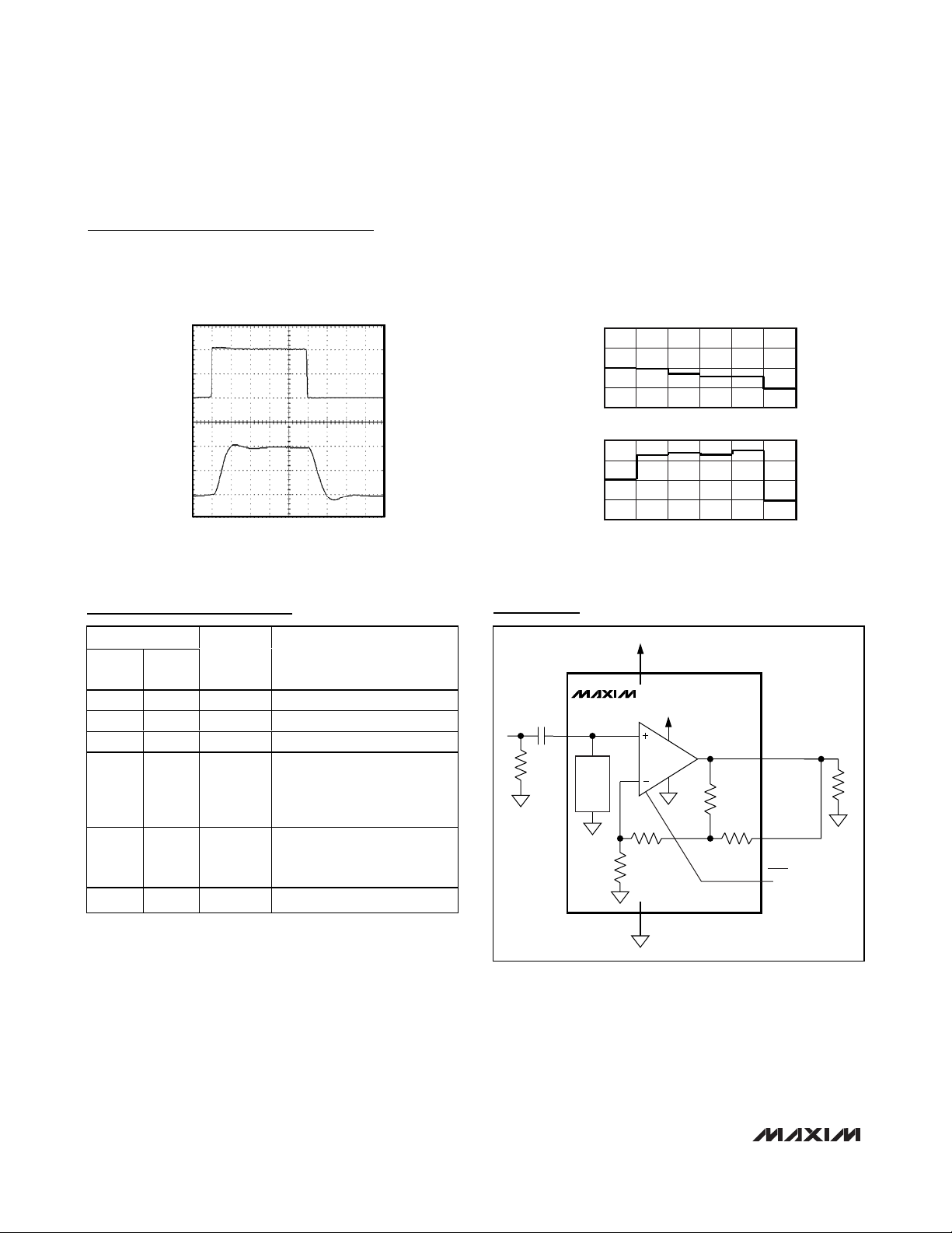
DIFFERENTIAL GAIN AND PHASE
-1.0
-2.0
0
1.0
2.0
DIFFERENTIAL
PHASE (°)
DIFFERENTIAL
GAIN (%)
MAX4090 toc18
0123456
0123456
-0.5
-1.0
0
0.5
1.0
Pin Description
Typical Application Circuit
V
25mV/div
V
OUT
50mV/div
IN
PIN
SOT23/
SC70
µDFN
1 4 OUT Video Output
2 2 GND Ground
3 3 IN Video Input
41V
55SHDN
6 6 FB Feedback. Connect to OUT.
SMALL-SIGNAL PULSE RESPONSE
10ns/div
MAX4090 toc17
NAME FUNCTION
Power-Supply Voltage. Bypass
with a 0.1µF capacitor to
CC
ground as close to pin as
possible.
Shutdown. Pull SHDN low to
place the MAX4090 in lowpower shutdown mode.
V
CC
MAX4090
IN
R
IN
CLAMP
GND
OUT
FB
SHDN
R
L

MAX4090
3V/5V, 6dB Video Buffer with Sync-Tip Clamp
and 150nA Shutdown Current
_______________________________________________________________________________________ 7
Detailed Description
The MAX4090 3V/5V, 6dB video buffer with sync-tip
clamp and low-power shutdown mode is available in tiny
SOT23 and SC70 packages. The MAX4090 is designed
to drive DC-coupled, 150Ω back-terminated video loads
in portable video applications such as digital still cams,
portable DVD players, digital camcorders, PDAs, videoenabled cell phones, portable game systems, and notebook computers. The input clamp positions the video
waveform at the output and allows the MAX4090 to be
used as a DC-coupled output driver.
The MAX4090 operates from a single 2.7V to 5.5V supply and consumes only 6.5mA of supply current. The
low-power shutdown mode reduces the supply current
to 150nA, making the MAX4090 ideal for low-voltage,
battery-powered video applications.
The input signal to the MAX4090 is AC-coupled
through a capacitor into an active sync-tip clamp circuit, which places the minimum of the video signal at
approximately 0.38V. The output buffer amplifies the
video signal while still maintaining the 0.38V clamp voltage at the output. For example, if V
IN
= 0.38V, then
V
OUT
= 0.38V. If VIN= 1.38V, then V
OUT
= 0.38V + (2 x
1V) = 2.38V. The net result is that a 2V video output
signal swings within the usable output voltage range of
the output buffer when V
CC
= 3V.
Shutdown Mode
The MAX4090 features a low-power shutdown mode
(I
SHDN
= 150nA) for battery-powered/portable applica-
tions. Pulling the SHDN pin high enables the output.
Connecting the SHDN pin to ground (GND) disables
the output and places the MAX4090 into a low-power
shutdown mode.
Applications Information
Input Coupling the MAX4090
The MAX4090 input must be AC-coupled because the
input capacitor stores the clamp voltage. The MAX4090
requires a typical value of 0.1µF for the input clamp to
meet the Line Droop specification. A minimum of a
ceramic capacitor with an X7R temperature coefficient
is recommended to avoid temperature-related problems with Line Droop. For extended temperature operation, such as outdoor applications, or where the
impressed voltage is close to the rated voltage of the
capacitor, a film dielectric is recommended. Increasing
the capacitor value slows the clamp capture time.
Values above 0.5µF should be avoided since they do
not improve the clamp’s performance.
The active sync-tip clamp also requires that the input
impedance seen by the input capacitor be less than
100Ω typically to function properly. This is easily met
by the 75Ω input resistor prior to the input-coupling
capacitor and the back termination from a prior stage.
Insufficient input resistance to ground causes the
MAX4090 to appear to oscillate. Never operate the
MAX4090 in this mode.
Using the MAX4090 with the
Reconstruction Filter
In most video applications, the video signal generated
from the DAC requires a reconstruction filter to smooth
out the signal and attenuate the sampling aliases. The
MAX4090 is a direct DC-coupled output driver, which
can be used after the reconstruction filter to drive the
video signal. The driving load from the video DAC can
be varied from 75Ω to 300Ω. A low input impedance
(<100Ω) is required by the MAX4090 in normal operation, special care must be taken when a reconstruction
filter is used in front of the MAX4090.
For standard video signal, the video passband is about
6MHz and the system oversampling frequency is at
27MHz. Normally, a 9MHz BW lowpass filter can be
used for the reconstruction filter. This section demonstrates the methods to build simple 2nd- and 3rd-order
passive butterworth lowpass filters at the 9MHz cutoff
frequency and the techniques to use them with the
MAX4090 (Figures 1 and 4).
2nd-Order Butterworth Lowpass Filter Realization
Table 1 shows the normalized 2nd-order butterworth
LPF component values at 1rad/s with a source/load
impedance of 1Ω.
With the following equations, the L and C can be calculated for the cutoff frequency at 9MHz. Table 2 shows
the appropriated L and C values for different source/
load impedance, the bench measurement values for
the -3dB BW and attenuation at 27MHz. There is
approximately 20dB attenuation at 27MHz, which effectively attenuates the sampling aliases. The MAX4090
requires low input impedance for stable operation and
it does not like the reactive input impedance. For R1/R2
greater than 100Ω, a series resistor RIS(Figure 1)
Table 1. 2nd-Order Butterworth Lowpass
Filter Normalized Values
Rn1 = Rn2 (Ω)Cn1 (F) Ln1 (H)
1 1.414 1.414

MAX4090
between 20Ω to 100Ω is needed to isolate the input
capacitor (C4) to the filter to prevent the oscillation
problem.
Figure 2 shows the frequency response for R1 = R2 =
150Ω. At 6MHz, the attenuation is about 1.4dB. The
attenuation at 27MHz is about 20dB. Figure 3 shows
the multiburst response for R1 = R2 = 150Ω.
3rd-Order Butterworth Lowpass Filter Realization
If more flat passband and more stopband attenuation
are needed, a 3rd-order LPF can be used. The design
procedures are similar to the 2nd-order butterworth
LPF.
Table 3 shows the normalized 3rd-order butterworth
lowpass filter with the cutoff frequency at 1 rad/s and
the stopband frequency at 3 rad/s. Table 4 shows the
appropriated L and C values for different source/load
impedance and the bench measurement values for
-3dB BW and attenuation at 27MHz. The attenuation is
over 40dB at 27MHz. At 6MHz, the attenuation is
approximately 0.6dB for R1 = R2 = 150Ω (Figure 5).
3V/5V, 6dB Video Buffer with Sync-Tip Clamp
and 150nA Shutdown Current
8 _______________________________________________________________________________________
Figure 1. 2nd-Order Butterworth LPF with MAX4090
Figure 2. Frequency Response
Figure 3. Multiburst Response
C
C
n
==
fR
22ππ
CL
LR
nL
L
f
C
2-POLE RECONSTRUCTION LPF
L1
C1
150pF
3.9μH
R2
150Ω
VIDEO
CURRENT
DAC
150Ω
R1
C7
1μF
R
49.9Ω
V
C4
IS
0.1μF
CC
V
CC
IN OUT
MAX4090
SHDN
GND
FB
R3
75Ω
V
CC
V
OUT
FREQUENCY RESPONSE
0
-10
-20
-30
GAIN (dB)
-40
-50
-60
0.1 1 10 100
FREQUENCY (MHz)
10μs/div
V
IN
500mV/div
V
OUT
500mV/div

MAX4090
3V/5V, 6dB Video Buffer with Sync-Tip Clamp
and 150nA Shutdown Current
_______________________________________________________________________________________ 9
Table 2. Bench Measurement Values
Table 3. 3rd-Order Butterworth Lowpass
Filter Normalized Values
Figure 4. 3rd-Order Butterworth LPF with MAX4090
Table 4. Bench Measurement Values
Sag Correction
In a 5V application, the MAX4090 can use the sag configuration if an AC-coupled output video signal is
required. Sag correction refers to the low-frequency
compensation for the highpass filter formed by the
150Ω load and the output capacitor. In video applications, the cutoff frequency must be low enough to pass
the vertical sync interval to avoid field tilt. This cutoff
frequency should be less than 5Hz, and the coupling
capacitor must be very large in normal configuration,
typically > 220µF. In sag configuration, the MAX4090
eliminates the need for large coupling capacitors, and
instead requires two 22µF capacitors (Figure 6) to
reach the same performance as the large capacitor.
Bench experiments show that increasing the output
coupling capacitor C5 beyond 47µF does not improve
the performance. If the supply voltage is less than 4.5V,
the sag correction is not recommended for the
MAX4090.
3-POLE RECONSTRUCTION LPF
C3
6.8pF
L1
VIDEO
CURRENT
DAC
150Ω
R1
4.7μH
C1
120pFC2120pF
3dB
R1 = R2
(Ω)
75 330 1.8 0 8.7 20
150 150 3.9 50 9.0 20
200 120 4.7 50 9.3 22
300 82 8.2 100 8.7 20
C1
(p f ) L1(µH)
R
(Ω)
IS
(MHz)
BW
A T T EN U A T I O N
AT 27MHz
(dB)
R2
150Ω
C7
1μF
R
49.9Ω
V
C4
IS
0.1μF
CC
V
CC
IN OUT
MAX4090
SHDN
GND
FB
R3
75Ω
Rn1 = Rn2
(Ω)
1 0.923 0.923 0.06 1.846
Cn1 (F) Cn2 (F) Cn3 (F) Ln1 (H)
V
CC
V
OUT
R1 = R2 (Ω) C1 (pF) C2 (pF) C3 (pF) L (µH) RIS (Ω) 3dB BW (MHz)
75 220 220 15.0 2.2 0 9.3 43
150 120 120 6.8 4.7 50 8.9 50
300 56 56 3.3 10.0 100 9.0 45
ATTENUATION AT
27MHz (dB)

MAX4090
3V/5V, 6dB Video Buffer with Sync-Tip Clamp
and 150nA Shutdown Current
10 ______________________________________________________________________________________
Figure 5. Frequency Response for R1 = R2 = 150
Ω
Figure 6. Sag Correction Configuration
Layout and Power-Supply Bypassing
The MAX4090 operates from single 2.7V to 5.5V supply. Bypass the supply with a 0.1µF capacitor as close
to the pin as possible. Maxim recommends using
microstrip and stripline techniques to obtain full bandwidth. To ensure that the PC board does not degrade
the device’s performance, design it for a frequency
greater than 1GHz. Pay careful attention to inputs and
outputs to avoid large parasitic capacitance. Whether
or not you use a constant-impedance board, observe
the following design guidelines:
• Do not use wire-wrap boards; they are too inductive.
• Do not use IC sockets; they increase parasitic
capacitance and inductance.
• Use surface-mount instead of through-hole components for better, high-frequency performance.
• Use a PC board with at least two layers; it should be
as free from voids as possible.
• Keep signal lines as short and as straight as possible.
Do not make 90° turns; round all corners.
FREQUENCY RESPONSE
0
-10
-20
-30
GAIN (dB)
-40
-50
-60
0.1 1 10 100
FREQUENCY (MHz)
3-POLE RECONSTRUCTION LPF
6.8pF
V
CC
C3
C7
1μF
VIDEO
CURRENT
DAC
150Ω
L1
4.7μH
R1
C1
120pFC2120pF
R2
150Ω
R
49.9Ω
V
C4
IS
0.1μF
CC
V
CC
IN OUT
MAX4090
SHDN
GND
FB
C5
22μF
C6
22μF
R3
75Ω
V
OUT

MAX4090
3V/5V, 6dB Video Buffer with Sync-Tip Clamp
and 150nA Shutdown Current
______________________________________________________________________________________ 11
Figure 7. Typical Operating Circuit
Figure 8. AC-Coupled Output Circuit
Chip Information
TRANSISTOR COUNT: 755
PROCESS: BiCMOS
= 2.7V TO 5.5V
V
CC
R
SOURCE
75Ω
R
E
SIGNAL
75Ω
IN
R
SOURCE
75Ω
R
E
SIGNAL
75Ω
IN
C
0.1μF
C
0.1μF
V
CC
IN
IN
MAX4090
IN
CLAMP
GND
V
CC
MAX4090
IN
CLAMP
SHDN
OUT
FB
SHDN
OUT
R
OUT
75Ω
= 2.7V TO 5.5V
V
CC
R
OUT
75Ω
C
0.1μF
E
OUT
R
75Ω
330μF
BYP
L
C
BYP
0.1μF
R
75Ω
E
OUT
L
FB
GND

MAX4090
3V/5V, 6dB Video Buffer with Sync-Tip Clamp
and 150nA Shutdown Current
12 ______________________________________________________________________________________
Package Information
For the latest package outline information and land patterns, go to www.maxim-ic.com/packages. Note that a “+”, “#”, or “-” in the
package code indicates RoHS status only. Package drawings may show a different suffix character, but the drawing pertains to the
package regardless of RoHS status.
PACKAGE TYPE PACKAGE CODE DOCUMENT NO.
6 SOT23 U6F-6
21-0058
6 µDFN L622-1
21-0164
6 SC70 X6SN-1
21-0077

MAX4090
3V/5V, 6dB Video Buffer with Sync-Tip Clamp
and 150nA Shutdown Current
______________________________________________________________________________________ 13
Package Information (continued)
For the latest package outline information and land patterns, go to www.maxim-ic.com/packages. Note that a “+”, “#”, or “-” in the
package code indicates RoHS status only. Package drawings may show a different suffix character, but the drawing pertains to the
package regardless of RoHS status.

MAX4090
3V/5V, 6dB Video Buffer with Sync-Tip Clamp
and 150nA Shutdown Current
14 ______________________________________________________________________________________
Package Information (continued)
For the latest package outline information and land patterns, go to www.maxim-ic.com/packages. Note that a “+”, “#”, or “-” in the
package code indicates RoHS status only. Package drawings may show a different suffix character, but the drawing pertains to the
package regardless of RoHS status.
AAA
AAA
D
PIN 1
INDEX AREA
SAMPLE
MARKING
7
A1
A
E
L
b
A
A2
L
e
C
L
e
EVEN TERMINAL
A A
(N/2 -1) x e)
b
N
SOLDER
MASK
COVERAGE
1
C
L
e
ODD TERMINAL
PIN 1
0.10x45∞
L1
6, 8, 10L UDFN.EPS
L
PACKAGE OUTLINE,
6, 8, 10L uDFN, 2x2x0.80 mm
21-0164
1
2
B

MAX4090
3V/5V, 6dB Video Buffer with Sync-Tip Clamp
and 150nA Shutdown Current
______________________________________________________________________________________ 15
Package Information (continued)
For the latest package outline information and land patterns, go to www.maxim-ic.com/packages. Note that a “+”, “#”, or “-” in the
package code indicates RoHS status only. Package drawings may show a different suffix character, but the drawing pertains to the
package regardless of RoHS status.
COMMON DIMENSIONS
-
e b
0.65 BSC
0.40 BSC
MAX.
0.80
2.05
2.05
0.50
0.30±0.05
0.25±0.050.50 BSC8L822-1
0.20±0.03
(N/2 -1) x e
1.30 REF.
1.50 REF.
1.60 REF.
SYMBOL
A
A1
A2
D 1.95 2.00
E
L
L1
PACKAGE VARIATIONS
PKG. CODE
MIN.
0.70 0.75
0.15 0.20 0.25
0.020 0.025 0.035
1.95 2.00
0.30 0.40
0.10 REF.
N
6L622-1
10L1022-1
NOM.
PACKAGE OUTLINE,
6, 8, 10L uDFN, 2x2x0.80 mm
2
21-0164
2
B

MAX4090
3V/5V, 6dB Video Buffer with Sync-Tip Clamp
and 150nA Shutdown Current
16 ______________________________________________________________________________________
Package Information (continued)
For the latest package outline information and land patterns, go to www.maxim-ic.com/packages. Note that a “+”, “#”, or “-” in the
package code indicates RoHS status only. Package drawings may show a different suffix character, but the drawing pertains to the
package regardless of RoHS status.
SC70, 6L.EPS

MAX4090
3V/5V, 6dB Video Buffer with Sync-Tip Clamp
and 150nA Shutdown Current
Maxim cannot assume responsibility for use of any circuitry other than circuitry entirely embodied in a Maxim product. No circuit patent licenses are
implied. Maxim reserves the right to change the circuitry and specifications without notice at any time.
Maxim Integrated Products, 120 San Gabriel Drive, Sunnyvale, CA 94086 408-737-7600 ____________________ 17
© 2009 Maxim Integrated Products Maxim is a registered trademark of Maxim Integrated Products, Inc.
Revision History
REVISION
NUMBER
4 11/09 Added automotive part 1
REVISION
DATE
DESCRIPTION
PAGES
CHANGED
 Loading...