

General Description
The MAX4080/MAX4081 are high-side, current-sense
amplifiers with an input voltage range that extends from
4.5V to 76V making them ideal for telecom, automotive,
backplane, and other systems where high-voltage current monitoring is critical. The MAX4080 is designed for
unidirectional current-sense applications and the
MAX4081 allows bidirectional current sensing. The
MAX4081 single output pin continuously monitors the
transition from charge to discharge and avoids the
need for a separate polarity output. The MAX4081
requires an external reference to set the zero-current
output level (V
SENSE
= 0V). The charging current is rep-
resented by an output voltage from V
REF
to VCC, while
discharge current is given from V
REF
to GND.
For maximum versatility, the 76V input voltage range
applies independently to both supply voltage (V
CC
)
and common-mode input voltage (V
RS+
). High-side
current monitoring does not interfere with the ground
path of the load being measured, making the
MAX4080/MAX4081 particularly useful in a wide range
of high-voltage systems.
The combination of three gain versions (5V/V, 20V/V,
60V/V = F, T, S suffix) and a user-selectable, external
sense resistor sets the full-scale current reading and its
proportional output voltage. The MAX4080/MAX4081
offer a high level of integration, resulting in a simple,
accurate, and compact current-sense solution.
The MAX4080/MAX4081 operate from a 4.5V to 76V single supply and draw only 75µA of supply current. These
devices are specified over the automotive operating
temperature range (-40°C to +125°C) and are available
in a space-saving 8-pin µMAX or SO package.
Applications
Automotive (12V, 24V, or 42V Batteries)
48V Telecom and Backplane Current
Measurement
Bidirectional Motor Control
Power-Management Systems
Avalanche Photodiode and PIN-Diode Current
Monitoring
General System/Board-Level Current Sensing
Precision High-Voltage Current Sources
Features
♦ Wide 4.5V to 76V Input Common-Mode Range
♦ Bidirectional or Unidirectional I
SENSE
♦ Low-Cost, Compact, Current-Sense Solution
♦ Three Gain Versions Available
5V/V (MAX4080F/MAX4081F)
20V/V (MAX4080T/MAX4081T)
60V/V (MAX4080S/MAX4081S)
♦ ±0.1% Full-Scale Accuracy
♦ Low 100µV Input Offset Voltage
♦ Independent Operating Supply Voltage
♦ 75µA Supply Current (MAX4080)
♦ Reference Input for Bidirectional OUT (MAX4081)
♦ Available in a Space-Saving 8-Pin µMAX Package
MAX4080/MAX4081
76V, High-Side, Current-Sense Amplifiers with
Voltage Output
________________________________________________________________ Maxim Integrated Products 1
Pin Configurations
Ordering Information
19-2562; Rev 0; 10/02
For pricing, delivery, and ordering information, please contact Maxim Direct at 1-888-629-4642,
or visit Maxim’s website at www.maxim-ic.com.
EVALUATION KIT
AVAILABLE
Selector Guide appears at end of data sheet.
PART TEMP RANGE PIN-PACKAGE
MAX4080FAUA -40°C to +125°C 8 µMAX
MAX4080FASA -40°C to +125°C 8 SO
MAX4080TAUA -40°C to +125°C 8 µMAX
MAX4080TASA -40°C to +125°C 8 SO
MAX4080SAUA -40°C to +125°C 8 µMAX
MAX4080SASA -40°C to +125°C 8 SO
MAX4081FAUA -40°C to +125°C 8 µMAX
MAX4081FASA -40°C to +125°C 8 SO
MAX4081TAUA -40°C to +125°C 8 µMAX
MAX4081TASA -40°C to +125°C 8 SO
MAX4081SAUA -40°C to +125°C 8 µMAX
MAX4081SASA -40°C to +125°C 8 SO
TOP VIEW
RS+
N.C.
1
2
CC
MAX4080
3
4
87RS-
6
5
N.C.V
N.C.
OUTGND
RS+
N.C.
1
2
CC
MAX4081
3
4
87RS-
REF1AV
REF1B
6
OUTGND
5
μMAX/SO
μMAX/SO
MAX4080/MAX4081
76V, High-Side, Current-Sense Amplifiers with
Voltage Output
2 _______________________________________________________________________________________
ABSOLUTE MAXIMUM RATINGS
Stresses beyond those listed under “Absolute Maximum Ratings” may cause permanent damage to the device. These are stress ratings only, and functional
operation of the device at these or any other conditions beyond those indicated in the operational sections of the specifications is not implied. Exposure to
absolute maximum rating conditions for extended periods may affect device reliability.
VCCto GND............................................................-0.3V to +80V
RS+, RS- to GND....................................................-0.3V to +80V
OUT to GND.............-0.3V to the lesser of +18V or (V
CC
+ 0.3V)
REF1A, REF1B to GND
(MAX4081 Only)....-0.3V to the lesser of +18V or (V
CC
+ 0.3V)
Output Short Circuit to GND.......................................Continuous
Differential Input Voltage (V
RS
+ - VRS-)...............................±80V
Current into Any Pin..........................................................±20mA
Continuous Power Dissipation (T
A
= +70°C)
8-Pin µMAX (derate 4.5mW/°C above +70°C) .............362mW
8-Pin SO (derate 5.88mW/°C above +70°C)................471mW
Operating Temperature Range .........................-40°C to +125°C
Junction Temperature......................................................+150°C
Storage Temperature Range .............................-65°C to +150°C
Lead Temperature (soldering, 10s) .................................+300°C
DC ELECTRICAL CHARACTERISTICS
(VCC= V
RS+
= 4.5V to 76V, V
REF1A
= V
REF1B
= 5V (MAX4081 only), V
SENSE
= (V
RS+
- V
RS-
) = 0V, R
LOAD
= 100kΩ, TA= T
MIN
to
T
MAX
, unless otherwise noted. Typical values are at TA= +25°C.) (Notes 1, 2)
Operating Voltage Range V
Common-Mode Range C
Supply Current I
Leakage Current I
Input Bias Current I
Full-Scale Sense Voltage (Note 4) V
Input Offset Voltage V
Common-Mode Rejection Ratio
Power-Supply Rejection Ratio
OUT High Voltage
PARAMETER SYMBOL CONDITIONS MIN TYP MAX UNITS
CC
MVR
CC
RS+
RS+
Inferred from PSRR test 4.5 76 V
Inferred from CMRR test (Note 3) 4.5 76 V
MAX4080 75 190
MAX4081 103 190
= 76V 0.01 2 µA
, I
RS-VCC
, I
RS-VCC
VCC = V
no load
= 0V, V
= V
= 76V,
RS+
RS+
= 76V 5 12 µA
RS+
MAX4080F/MAX4081F ±1000
SENSE
MAX4080T/MAX4081T ±250
MAX4080S/MAX4081S ±100
MAX4080F/MAX4081F 5
MAX4080T/MAX4081T 20Gain A
V
MAX4080S/MAX4081S 60
TA = +25°C ±0.1 ±0.6
VCC = V
V
(Note 5)
RS+
= 48V
TA = -40°C to +85°C ±1Gain Accuracy ΔA
= T
MIN
to T
MAX
T
A
TA = +25°C ±0.1 ±0.6
OS
CMRR V
PSRR V
VCC = V
(Note 6)
CC
RS+
= 48V
RS+
= 48V, V
RS+
TA = -40°C to +85°C ±1
T
= T
MIN
to T
MAX
A
= 4.5V to 76V 100 124 dB
= 48V, VCC = 4.5V to 76V 100 122 dB
MAX4080F/MAX4081F,
= 1000mV
V
V
= 4.5V, V
CC
-
)
= 48V, V
V
REF1B
(sourcing) =
I
OUT
(V
CC
V
OH
REF1A
= 2.5V,
RS+
=
+500µA (Note 8)
SENSE
MAX4080T/MAX4081T,
= 250mV
V
SENSE
MAX4080S/MAX4081S,
V
= 100mV
SENSE
0.15 0.27 V
±1.2
±1.2
µA
mV
V/V
%
mV
MAX4080/MAX4081
76V, High-Side, Current-Sense Amplifiers with
Voltage Output
_______________________________________________________________________________________ 3
DC ELECTRICAL CHARACTERISTICS (continued)
(VCC= V
RS+
= 4.5V to 76V, V
REF1A
= V
REF1B
= 5V (MAX4081 only), V
SENSE
= (V
RS+
- V
RS-
) = 0V, R
LOAD
= 100kΩ, TA= T
MIN
to
T
MAX
, unless otherwise noted. Typical values are at TA= +25°C.) (Notes 1, 2)
OUT Low Voltage V
REF1A = REF1B Input Voltage
Range (MAX4081 Only)
REF1A Input Voltage Range
(MAX4081 Only)
REF1A Rejection Ratio
(MAX4081 Only)
REF/REF1A Ratio
(MAX4081 Only)
REF1A Input Impedance
(MAX4081 Only)
PARAMETER SYMBOL CONDITIONS MIN TYP MAX UNITS
(V
OL
(V
REF
GND)
REF1A
GND)
VCC = V
V
REF1A
2.5V, V
-1000mV (for
MAX4081 only)
-
Inferred from REF1A rejection ratio,
V
REF1A
-
Inferred from REF1A rejection ratio,
V
REF1B
VCC = V
V
REF1A
V
REF1A
V
CC
V
REF1B
= 48V,
RS+
= V
REF1B
=
SENSE
= V
REF1B
= GND
= 48V, V
RS+
= V
REF1B
= 10V, V
= V
= 48V (Note 2)
RS+
= GND 250 kΩ
I
=
I
100µA
SENSE
= 1.5V to 6V
REF1B
OUT
OUT
= GND,
(sinking) = 10µA 4 15
(sinking) =
= 0V,
1.5 6 V
312V
80 108 dB
0.497 0.500 0.503
23 55
mV
MAX4080/MAX4081
76V, High-Side, Current-Sense Amplifiers with
Voltage Output
4 _______________________________________________________________________________________
AC ELECTRICAL CHARACTERISTICS
(VCC= V
RS+
= 4.5V to 76V, V
REF1A
= V
REF1B
= 5V (MAX4081 only), V
SENSE
= (V
RS+
- V
RS-
) = 0V, R
LOAD
= 100kΩ, C
LOAD
= 20pF,
T
A
= T
MIN
to T
MAX
, unless otherwise noted. Typical values are at TA= +25°C.) (Notes 1, 2)
Note 1: All devices are 100% production tested at TA= +25°C. All temperature limits are guaranteed by design.
Note 2: V
REF
is defined as the average voltage of V
REF1A
and V
REF1B
. REF1B is usually connected to REF1A or GND.
V
SENSE
is defined as V
RS+
- V
RS-
.
Note 3: The common-mode range at the low end of 4.5V applies to the most positive potential at RS+ or RS-. Depending on the
polarity of V
SENSE
and the device’s gain, either RS+ or RS- can extend below 4.5V by the device’s typical full-scale value of
V
SENSE
.
Note 4: Negative V
SENSE
applies to MAX4081 only.
Note 5: V
SENSE
is:
MAX4080F, 10mV to 1000mV
MAX4080T, 10mV to 250mV
MAX4080S, 10mV to 100mV
MAX4081F, -500mV to +500mV
MAX4081T, -125mV to +125mV
MAX4081S, -50mV to +50mV
Note 6: V
OS
is extrapolated from the gain accuracy test for the MAX4080 and measured as (V
OUT
- V
REF
)/AVat V
SENSE
= 0V, for the
MAX4081.
Note 7: V
SENSE
is:
MAX4080F, 500mV
MAX4080T, 125mV
MAX4080S, 50mV
MAX4081F/T/S, 0V
V
REF1B
= V
REF1A
= 2.5V
Note 8: Output voltage is internally clamped not to exceed 18V.
Note 9: Output settles to within 1% of final value.
Note 10: The device will not experience phase reversal when overdriven.
Bandwidth BW
OUT Settling Time to 1% of Final
Value
Capacitive-Load Stability No sustained oscillations 500 pF
Output Resistance R
Power-Up Time V
Saturation Recovery Time (Notes 9,10) 50 µs
PARAMETER SYMBOL CONDITION MIN TYP MAX UNITS
MAX4080F/T/S 250
MAX4081F/T/S 150
= 100mV ( Note 9) 50 µs
S E NS E
OUT
V
= V
CC
48V, V
V
SENSE
V
SENSE
V
SENSE
= V
C C
=
RS+
= 2.5V
OUT
= 10mV to 100mV 20
= 100mV to 10mV 20
= 100mV 0.1 Ω
= 48V , V
RS +
kHz
µs
MAX4080/MAX4081
76V, High-Side, Current-Sense Amplifiers with
Voltage Output
_______________________________________________________________________________________ 5
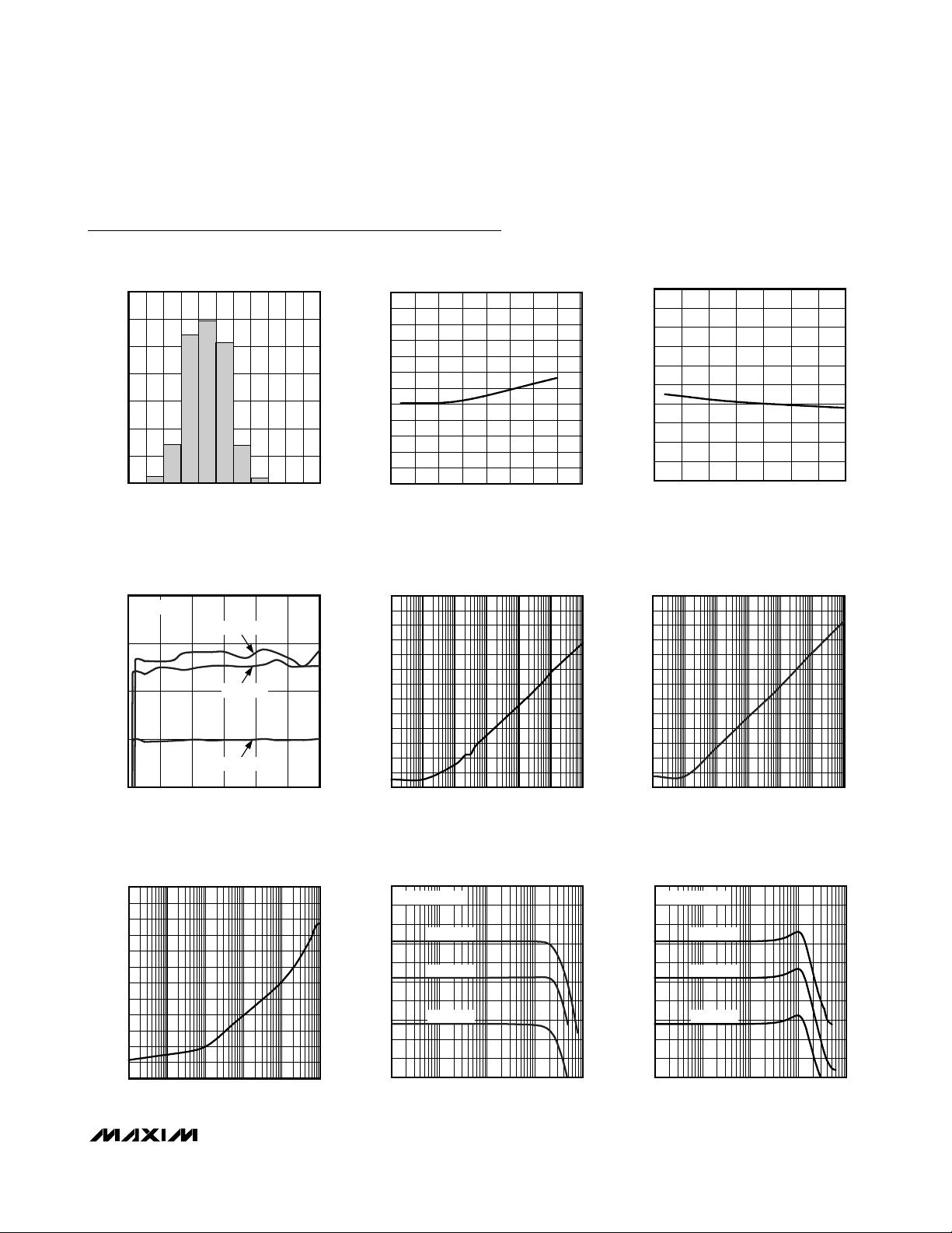
Typical Operating Characteristics
(VCC= V
RS+
= 48V, V
SENSE
= 0V, C
LOAD
= 20pF, R
LOAD
= ∞, TA= +25°C, unless otherwise noted.)
INPUT OFFSET VOLTAGE HISTOGRAM
35
30
25
20
15
PERCENTAGE (%)
10
5
0
-125 -75 -50 -25-100 0 25 50 75 100 125
INPUT OFFSET VOLTAGE (μV)
MAX4080 toc01
INPUT OFFSET VOLTAGE (μV)
300
250
200
150
100
50
0
-50
-100
-150
-200
-250
-300
-50 25 500-25
COMMON-MODE REJECTION RATIO
0
GAIN ACCURACY vs. V
V
= 48V
RS+
S VERSION
-0.05
-0.10
GAIN ACCURACY (%)
-0.15
-0.20
476
T VERSION
F VERSION
VCC (V)
CC
MAX4080 toc04
6452402816
0
-10
-20
-30
-40
-50
-60
-70
-80
-90
-100
-110
COMMON-MODE REJECTION RATIO (dB)
-120
-130
11M
MAX4081F/T/S
REFERENCE REJECTION RATIO
0
vs. FREQUENCY
-10
-20
-30
-40
-50
-60
-70
-80
-90
REFERENCE REJECTION RATIO (dB)
-100
-110
-120
FREQUENCY (Hz)
MAX4080 toc07
10k1k100101100k
SMALL-SIGNAL GAIN vs. FREQUENCY
50
V
SENSE
45
40
35
30
25
GAIN (dB)
20
15
10
5
0
0.1 1000
INPUT OFFSET VOLTAGE
vs. TEMPERATURE
TEMPERATURE (°C)
MAX4081F/T/S
vs. FREQUENCY
FREQUENCY (Hz)
MAX4080F/T/S
= 10mV
MAX4080S
MAX4080T
MAX4080F
FREQUENCY (kHz)
100 125 150
75
100101
100k10k1k10010
0.5
0.4
MAX4080 toc02
0.3
0.2
0.1
0
-0.1
GAIN ACCURACY (%)
-0.2
-0.3
-0.4
-0.5
-50 -25 0 25 50 75 100 125
0
-10
-20
MAX4080 toc05
-30
-40
-50
-60
-70
-80
-90
-100
-110
POWER-SUPPLY REJECTION RATIO (dB)
-120
-130
11M
50
45
MAX4080 toc08
40
35
30
25
GAIN (dB)
20
15
10
5
0
0.1 1000
GAIN ACCURACY vs. TEMPERATURE
TEMPERATURE (°C)
MAX4081F/T/S
POWER-SUPPLY REJECTION RATIO
vs. FREQUENCY
100k10k1k10010
FREQUENCY (Hz)
MAX4081F/T/S
SMALL-SIGNAL GAIN vs. FREQUENCY
V
= 100mV
OUT
P-P
MAX4081S
MAX4081T
MAX4081F
100101
FREQUENCY (kHz)
MAX4080 toc03
MAX4080 toc06
MAX4080 toc09

MAX4080/MAX4081
76V, High-Side, Current-Sense Amplifiers with
Voltage Output
6 _______________________________________________________________________________________
Typical Operating Characteristics (continued)
(VCC= V
RS+
= 48V, V
SENSE
= 0V, C
LOAD
= 20pF, R
LOAD
= ∞, TA= +25°C, unless otherwise noted.)
60
65
75
70
80
85
42816 40 52 64 76
MAX4080
SUPPLY CURRENT vs. V
CC
MAX4080 toc10
VCC (V)
SUPPLY CURRENT (μA)
NO LOAD
V
SENSE
= 0V
MAX4080 toc11
VCC (V)
SUPPLY CURRENT (μA)
645216 28 40
85
90
95
100
105
110
115
120
125
476
MAX4081
SUPPLY CURRENT vs. V
CC
V
REF
= 2.5V
NO LOAD
V
SENSE
= 0V
65
80
75
70
90
85
110
105
100
95
115
-50 -25 0 25 50 75 100 125
MAX4080
SUPPLY CURRENT vs. TEMPERATURE
MAX4080 toc12
TEMPERATURE (°C)
SUPPLY CURRENT (μA)
65
80
75
70
90
85
110
105
100
95
115
-50 -25 0 25 50 75 100 125
MAX4081
SUPPLY CURRENT vs. TEMPERATURE
MAX4080 toc13
TEMPERATURE (°C)
SUPPLY CURRENT (μA)
V
REF1A
= V
REF1B
= 2.5V
MAX4080 toc14
I
OUT
(SOURCING) (mA)
V
OUT
HIGH VOLTAGE (V
CC
- V
OH
) (V)
0.90.80.6 0.70.2 0.3 0.4 0.50.1
0.05
0.10
0.15
0.20
0.25
0.30
0.35
0.40
0.45
0.50
0
01.0
V
OUT
HIGH VOLTAGE
vs. I
OUT
(SOURCING)
VCC = 4.5V
TA = +125°C
TA = +85°C
TA = +25°C
TA = 0°C
TA = -40°C
45040035030025020015010050
50
100
150
200
250
300
0
0 500
V
OUT
LOW VOLTAGE
vs. I
OUT
(SINKING)
MAX4080 toc15
I
OUT
(SINKING) (μA)
V
OUT
LOW VOLTAGE (mV)
TA = +125°C
TA = +85°C
TA = +25°C
TA = 0°C
TA = -40°C
VCC = 4.5V
MAX4080 toc16
INPUT
5mV/div
OUTPUT
25mV/div
20μs/div
MAX4080F
SMALL-SIGNAL TRANSIENT RESPONSE
MAX4080 toc17
INPUT
5mV/div
OUTPUT
100mV/div
20μs/div
MAX4080T
SMALL-SIGNAL TRANSIENT RESPONSE
MAX4080 toc18
INPUT
5mV/div
OUTPUT
300mV/div
20μs/div
MAX4080S
SMALL-SIGNAL TRANSIENT RESPONSE

MAX4080/MAX4081
76V, High-Side, Current-Sense Amplifiers with
Voltage Output
_______________________________________________________________________________________ 7
Typical Operating Characteristics (continued)
(VCC= V
RS+
= 48V, V
SENSE
= 0V, C
LOAD
= 20pF, R
LOAD
= ∞, TA= +25°C, unless otherwise noted.)
INPUT
10mV/div
OUTPUT
50mV/div
INPUT
400mV/div
MAX4081F
SMALL-SIGNAL TRANSIENT RESPONSE
20μs/div
MAX4080 toc19
MAX4080F
LARGE-SIGNAL TRANSIENT RESPONSE
MAX4080 toc22
INPUT
2.5mV/div
OUTPUT
50mV/div
INPUT
100mV/div
MAX4081T
SMALL-SIGNAL TRANSIENT RESPONSE
20μs/div
MAX4080 toc20
MAX4080T
LARGE-SIGNAL TRANSIENT RESPONSE
MAX4080 toc23
SMALL-SIGNAL TRANSIENT RESPONSE
MAX4081S
INPUT
1mV/div
OUTPUT
50mV/div
20μs/div
MAX4080S
LARGE-SIGNAL TRANSIENT RESPONSE
INPUT
33mV/div
MAX4080 toc21
MAX4080 toc24
OUTPUT
2V/div
INPUT
400mV/div
OUTPUT
2V/div
20μs/div
MAX4081F
LARGE-SIGNAL TRANSIENT RESPONSE
20μs/div
MAX4080 toc25
OUTPUT
2V/div
INPUT
100mV/div
OUTPUT
2V/div
20μs/div
MAX4081T
LARGE-SIGNAL TRANSIENT RESPONSE
20μs/div
MAX4080 toc26
OUTPUT
2V/div
20μs/div
MAX4081S
LARGE-SIGNAL TRANSIENT RESPONSE
INPUT
33mV/div
OUTPUT
2V/div
20μs/div
MAX4080 toc27

MAX4080/MAX4081
76V, High-Side, Current-Sense Amplifiers with
Voltage Output
8 _______________________________________________________________________________________
Typical Operating Characteristics (continued)
(VCC= V
RS+
= 48V, V
SENSE
= 0V, C
LOAD
= 20pF, R
LOAD
= ∞, TA= +25°C, unless otherwise noted.)
MAX4080 toc28
4μs/div
VCC-TRANSIENT RESPONSE
V
CC
5V/div
V
OUT
1V/div
V
RS+
= 20V
V
CC
= 20V STEP
V
REF1
= V
REF2
= 2.5V
VCC = 40V
VCC = 20V
MAX4080 toc29
INPUT
500mV/div
OUTPUT
2V/div
20μs/div
MAX4080F
SATURATION RECOVERY RESPONSE
(V
CC
= 4.5V)
MAX4080 toc30
V
CC
(0 TO 10V)
5V/div
OUTPUT
2.5V/div
100μs/div
MAX4080T
STARTUP DELAY
(V
SENSE
= 250mV)

Detailed Description
The MAX4080/MAX4081 unidirectional and bidirectional
high-side, current-sense amplifiers feature a 4.5V to
76V input common-mode range that is independent of
supply voltage. This feature allows the monitoring of
current out of a battery as low as 4.5V and also enables
high-side current sensing at voltages greater than the
supply voltage (VCC). The MAX4080/MAX4081 monitors
current through a current-sense resistor and amplifies
the voltage across the resistor. The MAX4080 senses
current unidirectionally, while the MAX4081 senses current bidirectionally.
The 76V input voltage range of the MAX4080/MAX4081
applies independently to both supply voltage (VCC)
and common-mode, input-sense voltage (V
RS+
). Highside current monitoring does not interfere with the
ground path of the load being measured, making the
MAX4080/MAX4081 particularly useful in a wide range
of high-voltage systems.
Battery-powered systems require a precise bidirectional
current-sense amplifier to accurately monitor the battery’s charge and discharge. The MAX4081 charging
current is represented by an output voltage from V
REF
to VCC, while discharge current is given from V
REF
to
GND. Measurements of OUT with respect to V
REF
yield
a positive and negative voltage during charge and discharge, as illustrated in Figure 1 for the MAX4081T.
Current Monitoring
The MAX4080 operates as follows: current from the
source flows through R
SENSE
to the load (Figure 2), cre-
ating a sense voltage, V
SENSE
. Since the internal-sense
amplifier’s inverting input has high impedance, negligible
current flows through RG2 (neglecting the input bias
current). Therefore, the sense amplifier’s inverting input
voltage equals V
SOURCE
- (I
LOAD
)(R
SENSE
). The amplifier’s open-loop gain forces its noninverting input to the
same voltage as the inverting input. Therefore, the drop
across RG1 equals V
SENSE
. The internal current mirror
multiplies I
RG1
by a current gain factor, β, to give IA2=
β ✕ IRG1. Amplifier A2 is used to convert the output
current to a voltage and then sent through amplifier A3.
Total gain = 5V/V for MAX4080F, 20V/V for the
MAX4080T, and 60V/V for the MAX4080S.
The MAX4081 input stage differs slightly from the
MAX4080 (Figure 3). Its topology allows for monitoring
of bidirectional currents through the sense resistor.
When current flows from RS+ to RS-, the MAX4081
matches the voltage drop across the external sense
resistor, R
SENSE
, by increasing the current through the
Q1 and RG1. In this way, the voltages at the input terminals of the internal amplifier A1 are kept constant and
an accurate measurement of the sense voltage is
achieved. In the following amplifier stages of the
MAX4081, the output signal of amplifier A2 is levelshifted to the reference voltage (V
REF
= V
REF1A
=
V
REF1B
), resulting in a voltage at the output pin (OUT)
MAX4080/MAX4081
76V, High-Side, Current-Sense Amplifiers with
Voltage Output
_______________________________________________________________________________________ 9
Pin Description
PIN
MAX4080 MAX4081
1 1 RS+ Power connection to the external-sense resistor.
22 V
3, 6, 7 3 N.C. No Connection. No internal connection. Leave open or connect to ground.
4 4 GND Ground
5 5 OUT
8 8 RS- Load connection to the external sense resistor.
— 6 REF1B
— 7 REF1A
NAME FUNCTION
CC
Supply Voltage Input. Decouple V
bypass line transients.
Voltage Output. For the unidirectional MAX4080, V
V
. For the bidirectional MAX4081, the difference voltage (V
SENSE
proportional to V
Reference Voltage Input: Connect REF1B to REF1A or to GND (see the External
Reference section).
Reference Voltage Input: Connect REF1A and REF1B to a fixed reference
voltage (V
Reference section).
REF
). V
and indicates the correct polarity.
SENSE
is equal to V
OUT
to GND with at least a 0.1µF capacitor to
CC
when V
REF
is proportional to
OUT
is zero (see the External
SENSE
- V
REF
) is
OUT

MAX4080/MAX4081
that swings above V
REF
voltage for positive-sense volt-
ages and below V
REF
for negative-sense voltages.
V
OUT
is equal to V
REF
when V
SENSE
is equal to zero.
Set the full-scale output range by selecting R
SENSE
and
the appropriate gain version of the MAX4080/
MAX4081.
76V, High-Side, Current-Sense Amplifiers with
Voltage Output
10 ______________________________________________________________________________________
Figure 1. MAX4081T OUT Transfer Curve
Figure 3. MAX4081 Functional Diagram
Figure 2. MAX4080 Functional Diagram
I
4.5V TO 76V
BATTERY
LOAD
V
CC
V
SENSE
R
SENSE
MAX4081T
GND
RS+RS-
REF1A
REF1B
V
I
LOAD
CURRENT
MIRROR
SENSE
R
SENSE
RS+
R
G1
RS-
R
G2
MAX4080
A1
Q1
I
A2
A3A2
I
CHARGE
OUT
SYSTEM LOAD
AND CHARGER
5V
OUT
10V
5V
-250mV 250mV
= GND
V
OUT
DISCHARGE CURRENT
RS+
R
Q1 Q2
CURRENT
MIRROR
-5V
V
SENSE
RS-
G1
R
G2
A1
CURRENT
MIRROR
CHARGE CURRENT
REF
- V
OUT
V
V
REF1A
V
= 10V
OUT
V
SENSE
= V
REF1B
MAX4081
= 5V
RF
A2
OUT
125kΩ
REF1B
125kΩ
REF1A
GND
V
REF

MAX4080/MAX4081
76V, High-Side, Current-Sense Amplifiers with
Voltage Output
______________________________________________________________________________________ 11
Table 1. Typical Component Values
External References (MAX4081)
For the bidirectional MAX4081, the V
OUT
reference level
is controlled by REF1A and REF1B. V
REF
is defined as
the average voltage of V
REF1A
and V
REF1B
. Connect
REF1A and REF1B to a low-noise, regulated voltage
source to set the output reference level. In this mode,
V
OUT
equals V
REF1A
when V
SENSE
equals zero (see
Figure 4).
Alternatively, connect REF1B to ground, and REF1A to a
low-noise, regulated voltage source. In this case, the output reference level (V
REF
) is equal to V
REF1A
divided by
two. V
OUT
equals V
REF1A
/2 when V
SENSE
equals zero.
In either mode, the output swings above the reference
voltage for positive current-sensing (V
RS+
> V
RS-
). The
output swings below the reference voltage for negative
current-sensing (V
RS+
< V
RS-
).
Applications Information
Recommended Component Values
Ideally, the maximum load current develops the fullscale sense voltage across the current-sense resistor.
Choose the gain needed to yield the maximum output
voltage required for the application:
V
OUT
= V
SENSE
✕ A
V
where V
SENSE
is the full-scale sense voltage, 1000mV
for gain of 5V/V, 250mV for gain of 20V/V, 100mV for
gain of 60V/V, and AVis the gain of the device.
In applications monitoring a high current, ensure that
R
SENSE
is able to dissipate its own I2R loss. If the resistor’s power dissipation is exceeded, its value may drift
or it may fail altogether.
The MAX4080/MAX4081 sense a wide variety of currents with different sense-resistor values. Table 1 lists
common resistor values for typical operation.
FULL-SCALE LOAD
CURRENT, I
0.500 1000 5 ±500 ±2.5
0.125 1000 20 ±125 ±2.5
0.050 1000 60 ±50 ±3.0
5.000 100 5 ±500 ±2.5
1.250 100 20 ±125 ±2.5
0.500 100 60 ±50 ±3.0
50.000 10 5 ±500 ±2.5
12.500 10 20 ±125 ±2.5
5.000 10 60 ±50 ±3.0
FULL-SCALE LOAD
CURRENT, I
1.000 1000 5 1000 5.0
0.250 1000 20 250 5.0
0.100 1000 60 100 6.0
10.000 100 5 1000 5.0
2.500 100 20 250 5.0
1.000 100 60 100 6.0
50.000 10 5 500 2.5
25.000 10 20 250 5.0
10.000 10 60 100 6.0
LOAD
LOAD
(A)
(A)
CURRENT-SENSE
RESISTOR (mΩ)
CURRENT-SENSE
RESISTOR (mΩ)
GAIN
(V/V)
GAIN
(V/V)
FULL-SCALE
V
SENSE
(mV)
FULL-SCALE
V
SENSE
(mV)
MAX4081 FULL-SCALE
OUTPUT VOLTAGE
(V
- V
OUT
MAX4080 FULL-SCALE
OUTPUT VOLTAGE (V)
REF,
V)

MAX4080/MAX4081
The full-scale output voltage is V
OUT
= R
SENSE
✕ I
LOAD
(MAX)
✕ A
V
, for the MAX4080 and V
OUT
= V
REF
±
R
SENSE
✕ I
LOAD(MAX)
✕ A
V
for the MAX4081.
V
SENSE(MAX)
is 1000mV for the 5V/V gain version,
250mV for the 20V/V gain version, and 100mV for the
60V/V gain version.
Choosing the Sense Resistor
Choose R
SENSE
based on the following criteria:
• Voltage Loss: A high R
SENSE
value causes the
power-source voltage to degrade through IR loss. For
minimal voltage loss, use the lowest R
SENSE
value.
• Accuracy: A high R
SENSE
value allows lower currents to be measured more accurately. This is due to
offsets becoming less significant when the sense
voltage is larger. For best performance, select
R
SENSE
to provide approximately 1000mV (gain of
5V/V), 250mV (gain of 20V/V), or 100mV (gain of
60V/V) of sense voltage for the full-scale current in
each application.
• Efficiency and Power Dissipation: At high current
levels, the I2R losses in R
SENSE
can be significant.
Take this into consideration when choosing the
resistor value and its power dissipation (wattage)
rating. Also, the sense resistor’s value might drift if it
is allowed to heat up excessively.
• Inductance: Keep inductance low if I
SENSE
has a
large high-frequency component. Wire-wound resistors have the highest inductance, while metal film is
somewhat better. Low-inductance, metal-film resistors are also available. Instead of being spiralwrapped around a core, as in metal-film or wirewound resistors, they are a straight band of metal
and are available in values under 1Ω.
Because of the high currents that flow through R
SENSE
,
take care to eliminate parasitic trace resistance from
causing errors in the sense voltage. Either use a fourterminal current-sense resistor or use Kelvin (force and
sense) PC board layout techniques.
Dynamic Range Consideration
Although the MAX4081 have fully symmetrical bidirectional V
SENSE
input capability, the output voltage range
is usually higher from REF to VCCand lower from REF
to GND (unless the supply voltage is at the lowest end
of the operating range). Therefore, the user must consider the dynamic range of current monitored in both
directions and choose the supply voltage and the reference voltage (REF) to make sure the output swing
above and below REF is adequate to handle the swings
without clipping or running out of headroom.
Power-Supply Bypassing and Grounding
For most applications, bypass VCCto GND with a 0.1µF
ceramic capacitor. In many applications, VCCcan be
connected to one of the current monitor terminals (RS+
or RS-). Because VCCis independent of the monitored
voltage, VCCcan be connected to a separate regulated
supply.
If VCCwill be subject to fast-line transients, a series
resistor can be added to the power-supply line of the
MAX4080/MAX4081 to minimize output disturbance.
This resistance and the decoupling capacitor reduce
the rise time of the transient. For most applications, 1kΩ
in conjunction with a 0.1µF bypass capacitor work well.
The MAX4080/MAX4081 require no special considerations with respect to layout or grounding. Consideration
should be given to minimizing errors due to the large
charge and discharge currents in the system.
76V, High-Side, Current-Sense Amplifiers with
Voltage Output
12 ______________________________________________________________________________________
Figure 4. MAX4081 Reference Inputs
I
LOAD
= 0
I
LOAD
= 0
R
SENSE
RS-RS+
V
CC
MAX4081
GND
REF1A
REF1B
OUT
LOAD
5V
5V
R
V
CC
GND
SENSE
RS-RS+
REF1A
MAX4081
REF1B
OUT
LOAD
10V
5V
Power Management
The bidirectional capability of the MAX4081 makes it an
excellent candidate for use in smart battery packs. In
the application diagram (Figure 5), the MAX4081 monitors the charging current into the battery as well as the
discharge current out of the battery. The microcontroller stores this information, allowing the system to
query the battery's status as needed to make system
power-management decisions.
MAX4080/MAX4081
76V, High-Side, Current-Sense Amplifiers with
Voltage Output
______________________________________________________________________________________ 13
Typical Operating Circuit
Chip Information
TRANSISTOR COUNT: 185
PROCESS: Bipolar
Selector Guide
Figure 5. MAX4081 Used In Smart-Battery Application
PART GAIN (V/V) I
MAX4080FAUA 5 Unidirectional
MAX4080FASA 5 Unidirectional
MAX4080TAUA 20 Unidirectional
MAX4080TASA 20 Unidirectional
MAX4080SAUA 60 Unidirectional
MAX4080SASA 60 Unidirectional
MAX4081FAUA 5 Bidirectional
MAX4081FASA 5 Bidirectional
MAX4081TAUA 20 Bidirectional
MAX4081TASA 20 Bidirectional
MAX4081SAUA 60 Bidirectional
MAX4081SASA 60 Bidirectional
SENSE
R
SENSE
RS-RS+
V
CC
MAX4081
REF1A
GND
1.8V
OUT
ADC
MAX1243
μC
REF1B
SYSTEM
POWER
MANAGEMENT
AND
CHARGER
CIRCUITRY
SERIAL
INTERFACE
I
SENSE
VCC = 4.5V TO 76V
R
SENSE
V
CC
SYSTEM
LOAD
RS-RS+
BATTERY
MAX4080
OUT
GND

MAX4080/MAX4081
76V, High-Side, Current-Sense Amplifiers with
Voltage Output
14 ______________________________________________________________________________________
Package Information
(The package drawing(s) in this data sheet may not reflect the most current specifications. For the latest package outline information,
go to www.maxim-ic.com/packages.)
8
b
E H
A1
A
Ø0.50±0.1
0.6±0.1
0.6±0.1
1
D
TOP VIEW
A2
e
FRONT VIEW
4X S
c
L
BOTTOM VIEW
SIDE VIEW
8
1
DIM
A
A1
A2
b
c
D
e
E
H
L
α
S
INCHES
MIN
-
0.002
0.030
0.010
0.005
0.116
0.0256 BSC
0.116
0.188
0.016
0°
0.0207 BSC
MAX
0.043
0.006
0.037
0.014
0.007
0.120
0.120
0.198
0.026
6°
MILLIMETERS
MIN
0.05 0.15
0.25 0.36
0.13 0.18
2.95 3.05
2.95 3.05
4.78
0.41
MAX
- 1.10
0.950.75
0.65 BSC
5.03
0.66
0.5250 BSC
8LUMAXD.EPS
6°0°
α
PROPRIETARY INFORMATION
TITLE:
PACKAGE OUTLINE, 8L uMAX/uSOP
21-0036
REV.DOCUMENT CONTROL NO.APPROVAL
1
J
1

MAX4080/MAX4081
76V, High-Side, Current-Sense Amplifiers with
Voltage Output
Maxim cannot assume responsibility for use of any circuitry other than circuitry entirely embodied in a Maxim product. No circuit patent licenses are
implied. Maxim reserves the right to change the circuitry and specifications without notice at any time.
Maxim Integrated Products, 120 San Gabriel Drive, Sunnyvale, CA 94086 408-737-7600 ____________________ 15
© 2002 Maxim Integrated Products is a registered trademark of Maxim Integrated Products.
Package Information (continued)
(The package drawing(s) in this data sheet may not reflect the most current specifications. For the latest package outline information,
go to www.maxim-ic.com/packages.)
N
1
e
TOP VIEW
D
FRONT VIEW
INCHES
DIM
MIN
0.053A
0.004
A1
0.014
B
0.007
C
e 0.050 BSC 1.27 BSC
0.150
HE
A
B
A1
C
L
E
H 0.2440.228 5.80 6.20
0.016L
VARIATIONS:
INCHES
MINDIM
D
0.189 0.197 AA5.004.80 8
0.337 0.344 AB8.758.55 14
D
0∞-8∞
SIDE VIEW
MAX
0.069
0.010
0.019
0.010
0.157
0.050
MAX
0.3940.386D
MILLIMETERS
MAX
MIN
1.35
1.75
0.10
0.25
0.35
0.49
0.19
0.25
3.80 4.00
0.40 1.27
MILLIMETERS
MAX
MIN
9.80 10.00
N MS012
16
AC
SOICN .EPS
PROPRIETARY INFORMATION
TITLE:
PACKAGE OUTLINE, .150" SOIC
21-0041
REV.DOCUMENT CONTROL NO.APPROVAL
1
B
1
 Loading...