

General Description
The MAX4079 filters and buffers video (NTSC/PAL/DVB)
and stereo audio signals from the MPEG decoder of a
cable/satellite receiver, VCR/DVD player, or a TV to an
external load. The MAX4079 has luma-chroma (Y-C)
and composite (CVBS) video inputs with one Y-C and
two CVBS outputs. All video inputs are AC-coupled with
internal DC biasing on the chroma input and active
clamps for the luma and composite.
The MAX4079 video reconstruction filters have a 6MHz
cutoff frequency and 50dB attenuation at 27MHz. The
filters are matched with flat group delay for standarddefinition video. The video gain is fixed at +6dB to drive
a 75Ω back-terminated load (150Ω) to unity gain. The
video outputs can be either DC- or AC-coupled and are
powered by a single +5V supply.
The MAX4079 audio amplifiers have differential inputs
for optimum performance, but can be used with singleended sources with external biasing. The audio channels have a fixed gain of +6dB and deliver 2.6V
RMS
output with a differential input of ±1.85V. The audio
amplifiers operate from a +9V to +12V single supply
and feature an internal bias generator. An on-chip
mixer also provides a mono output, with +3dB gain,
derived from the left and right audio channels.
The MAX4079 is available in 24-pin TSSOP package,
and is fully specified over the 0°C to +70°C commercial
temperature range. The MAX4079 Evaluation Kit is
available to help speed designs.
Applications
Satellite Receivers
Cable Receivers
Home Theater Systems
DVD Players
AV Receivers
Televisions
Features
♦ Integrated Video Reconstruction Filters—6MHz
Lowpass Filter Supports NTSC, PAL, or DVB per
ITU-601
♦ Integrated Video and Audio Amplifiers
♦ Integrated Video Input Clamps and Biasing
♦ Mono Audio and CVBS Output to Drive External
Modulator
♦ +5V (Video) and +9V to +12V (Audio) Single-
Supply Operation
♦ Differential/Single-Ended Audio Inputs
♦ 24-Pin TSSOP Package
MAX4079
Complete Audio/Video
Backend Solution
________________________________________________________________
Maxim Integrated Products
1
Ordering Information
19-3780; Rev 1; 3/09
EVALUATION KIT
AVAILABLE
+
Denotes lead(Pb)-free package.
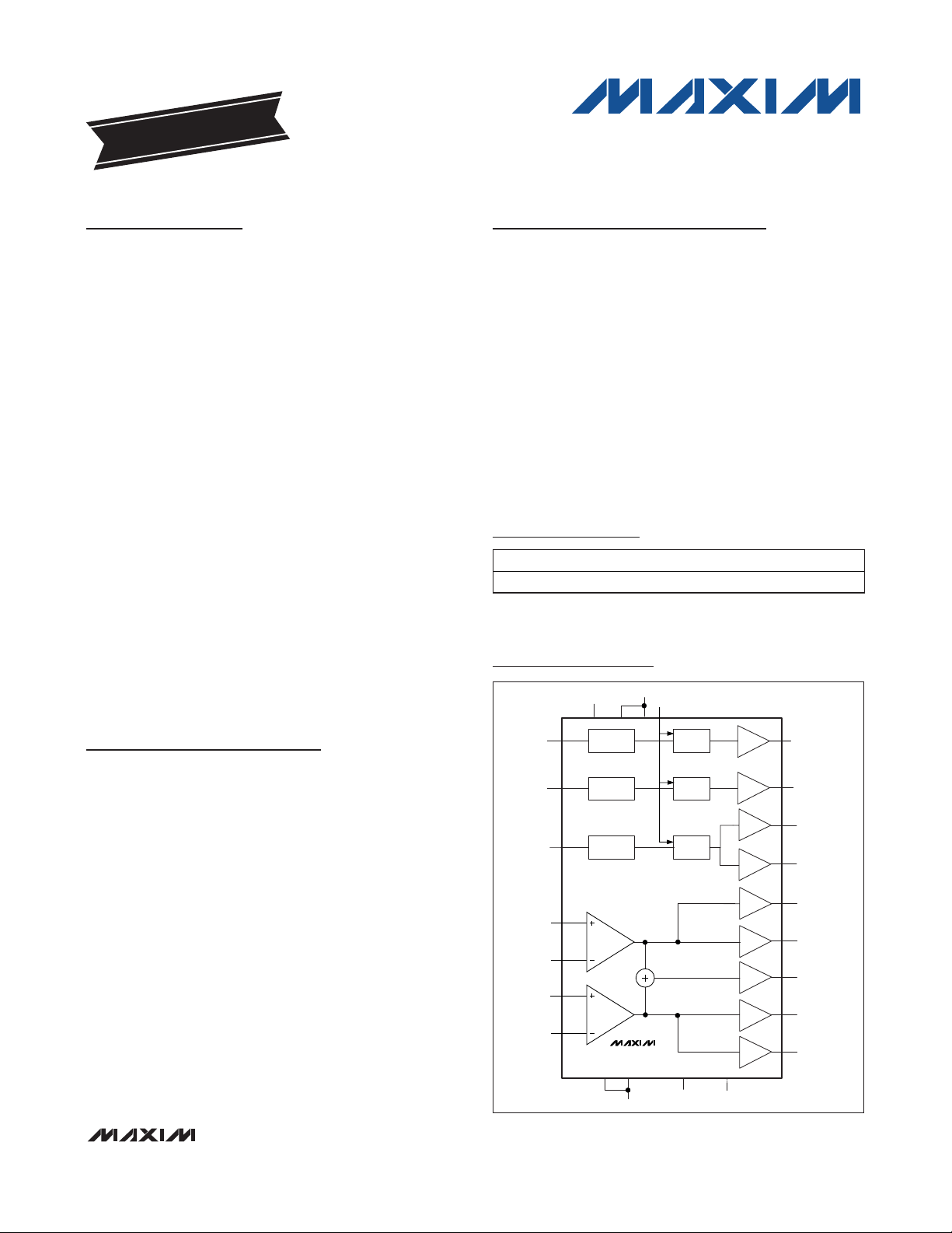
Functional Diagram
LP
FILTER
CLAMP
BIAS
NETWORK
CLAMP
RINP
RINN
LINP
LINN
CIN
CVBSIN
YIN
COUT
CVBSOUT1
CVBSOUT2
ROUT1
ROUT2
MONO
LOUT1
LOUT2
GVID
GAUD
VVID
AUDV
REXT
CBYPASS
+3dB
+6dB
+6dB
+6dB
+6dB
+6dB
+6dB
+6dB
+6dB
YOUT
LP
FILTER
LP
FILTER
MAX4079
Pin Configuration appears at end of data sheet.
For pricing, delivery, and ordering information, please contact Maxim Direct at 1-888-629-4642,
or visit Maxim’s website at www.maxim-ic.com.
PART TEMP RANGE PIN-PACKAGE
MAX4079CUG+ 0°C to +70°C 24 TSSOP
MAX4079
Complete Audio/Video
Backend Solution
2 _______________________________________________________________________________________
ABSOLUTE MAXIMUM RATINGS
Stresses beyond those listed under “Absolute Maximum Ratings” may cause permanent damage to the device. These are stress ratings only, and functional
operation of the device at these or any other conditions beyond those indicated in the operational sections of the specifications is not implied. Exposure to
absolute maximum rating conditions for extended periods may affect device reliability.
GVID to GAUD.......................................................-0.1V to +0.1V
VVID to GVID ............................................................-0.3V to +6V
AUDV to GAUD ......................................................-0.3V to +14V
LINP, LINN, RINP, RINN, CBYPASS to GAUD .........-0.3V to +6V
LOUT1, LOUT2, ROUT1, ROUT2,
MONO to GAUD ......-0.3V to lower of (+9V and AUDV + 0.3V)
YIN, CIN, CVBSIN, REXT to GVID.............-0.3V to (VVID + 0.3V)
YOUT, COUT, CVBSOUT1, CVBSOUT2 to
GVID.......................................................-0.3V to (VVID + 0.3V)
Video Output Short-Circuit Duration to GVID or
VVID ........................................................................Continuous
Audio Output Short-Circuit Duration to GAUD or
AUDV.......................................................................Continuous
Continuous Power Dissipation (T
A
= +70°C)
24-Pin TSSOP (derate 12.2mW/°C above +70°C) .....975.6mW
Operating Temperature Range...............................0°C to +70°C
Storage Temperature Range .............................-65°C to +150°C
Junction Temperature......................................................+150°C
Lead Temperature (soldering, 10s) .................................+300°C
DC ELECTRICAL CHARACTERISTICS
(V
VVID
= +5V, V
AUDV
= +12V, V
GVID
= V
GAUD
= 0V, R
LOAD_VID
= 150Ω to GVID, R
REXT
= 10kΩ ±1%, C
CBYPASS
= 1µF, TA= 0°C to
+70°C, unless otherwise noted. Typical values are at T
A
= +25°C.) (Note 1)
SUPPLIES
Audio Supply Voltage Range AUDV 8.5 12.6 V
Video Supply Voltage Range VVID 4.75 5.0 5.25 V
Video Quiescent Supply Current I
Audio Quiescent Supply Current I
Thermal Shutdown T
Thermal-Shutdown Hysteresis T
VIDEO
Voltage Gain A
Gain Matching ΔA
Input Voltage Swing V
Clamp Voltage V
Chroma Bias V
Droop D (Note 2) 2 %
REXT Reference Voltage V
Input Resistance R
Input Clamping Current I
Output Voltage Swing V
Short-Circuit Current I
Power-Supply Rejection Ratio PSRR
PARAMETER SYMBOL CONDITIONS MIN TYP MAX UNITS
CCV
CCA
SD,HYS
V,VID
V,VIDVIN
IN,VID
CLMP
BIAS
REXT
IN,VID
CLMP
OUT,VID
SC,VID
SD
V
= 5.25V, no load, all video inputs
VVID
AC-coupled to ground
V
= 12.6V, no load, audio inputs
AUDV
biased at 2.5V
Rising die temperature +150 °C
VIN = 1V
YIN, CVBSIN 0 1.2
CIN 0 0.9
CVBSOUT_ and YOUT, no signal, no load 1.0 V
COUT, no signal, no load 2.1 V
CVBSIN or YIN 2.3 MΩ
CIN 10 kΩ
CVBSIN or YIN input, VIN = 3.5V 1 2.5 4 µA
CVBSOUT_, YOUT 2.4
COUT 1.8
Video output shorted to VVID or GVID 50 mA
4.75V ≤ V
VID
5.25V
= 1V
P-P
P-P
VVID
, all video inputs, no load 5.8 6 6.2 dB
, all video inputs, no load -0.4 +0.4 dB
YOUT/COUT 48
≤
CVBSOUT_ 48
0.85 1.00 1.15 V
60 100 mA
815mA
25 °C
V
P-P
V
P-P
dB
MAX4079
Complete Audio/Video
Backend Solution
_______________________________________________________________________________________ 3
DC ELECTRICAL CHARACTERISTICS (continued)
(V
VVID
= +5V, V
AUDV
= +12V, V
GVID
= V
GAUD
= 0V, R
LOAD_VID
= 150Ω to GVID, R
REXT
= 10kΩ ±1%, C
CBYPASS
= 1µF, TA= 0°C to
+70°C, unless otherwise noted. Typical values are at T
A
= +25°C.) (Note 1)
AC ELECTRICAL CHARACTERISTICS
(V
VVID
= +5V, V
AUDV
= +12V, V
GVID
= V
GAUD
= 0V, R
IN_VIDEO
= 75Ω to GVID, C
IN_VIDEO
= 0.1µF, R
LOAD_VID
= 150Ω to GVID,
C
OUT_AUDIO
= 10µF, R
LOAD_AUD
= 10kΩ ±1% to GAUD, R
REXT
= 10kΩ, C
CBYPASS
= 1µF, TA= 0°C to +70°C, unless otherwise
noted. Typical values are at T
A
= +25°C.) (Note 1)
PARAMETER SYMBOL CONDITIONS MIN TYP MAX UNITS
AUDIO
Voltage Gain A
Mono Voltage Gain A
Gain Matching Between
Channels
Input Voltage Range V
Differential Input Voltage Range V
Input Current I
Output Voltage Swing V
Short-Circuit Current I
V,AUD
V,MONO
ΔA
V,AUD
IN,AUD
IN,AUD DIF
IN,AUD
OUT,AUD
SC,AUD
Power-Supply Rejection Ratio PSRR
Common-Mode Rejection Ratio CMRR
1.414V
1.414V
1.414V
differential input 5.8 6 6.2 dB
P-P
differential input, LIN = R
P-P
differential input -0.4 +0.4 dB
P-P
Inferred from CMRR test 0.3 5.2 V
Inferred from output voltage swing -1.85 +1.85 V
Input overdriven, 10kΩ load to 4.15V 7.4 V
8.5V ≤ V
AUD
0.3V ≤ VCM ≤ 5.2V 50 60 dB
AUD
≤ 12.6V 70 dB
AUDV
PARAMETER SYMBOL CONDITIONS MIN TYP MAX UNITS
VIDEO
Filter Attenuation A
Slew Rate SR V
Differential Gain DG
Differential Phase DP
Power-Supply Rejection Ratio PSRR
Peak Signal to RMS Noise SNR
Group Delay Deviation GD
Output Impedance Z
Capacitive Load C
Video Crosstalk X
Audio/Video Crosstalk X
CVBSOUT1 = CVBSOUT2 =
YOUT = COUT = 2V
VIDEO
R
attenuation is referred to
100kHz
CVBSOUT_, YOUT, COUT, 5-step
modulated staircase
CVBSOUT_, YOUT, COUT, 5-step
modulated staircase
f = 100kHz, 0.5V
VID
VID
CVBSOUT_, YOUT, COUT, VIN = 1V
CVBSOUT_, YOUT, COUT, f
4.5MHz
OUT,VID
L,VID
TALK,VID
TALK,VD/AD
f = 3.58MHz 0.5 Ω
No sustained oscillations 35 pF
f = 3.58MHz, 1V
active inputs
f = 15kHz, 1V
active audio or video inputs
= 150Ω to ground,
L
= 2V
OUT
P-P
P-P
P-P
P-P
P-P
input, between any two
input, between any two
IN
;
f = 4MHz -0.5 +0.5
2.8 3 3.2 dB
f = 7MHz 3
f = 27MHz 40 50
YOUT/COUT 48
CVBSOUT_ 44
P-P
= 0.1MHz to
IN
2µA
15 mA
30 V/µs
0.5 %
0.9 degrees
65 dB
25 ns
-63
-76
P-P
dB
dB
dB
MAX4079
Complete Audio/Video
Backend Solution
4 _______________________________________________________________________________________
AC ELECTRICAL CHARACTERISTICS (continued)
(V
VVID
= +5V, V
AUDV
= +12V, V
GVID
= V
GAUD
= 0V, R
IN_VIDEO
= 75Ω to GVID, C
IN_VIDEO
= 0.1µF, R
LOAD_VID
= 150Ω to GVID,
C
OUT_AUDIO
= 10µF, R
LOAD_AUD
= 10kΩ ±1% to GAUD, R
REXT
= 10kΩ, C
CBYPASS
= 1µF, TA= 0°C to +70°C, unless otherwise
noted. Typical values are at T
A
= +25°C.) (Note 1)
Note 1: All devices are 100% production tested at TA= +25°C. Specifications over temperature limits are guaranteed by design.
Note 2: Droop is defined as the percentage change in the DC level from the start to the end of a video line. Inferred from input
clamping current with a 0.1µF coupling capacitor.
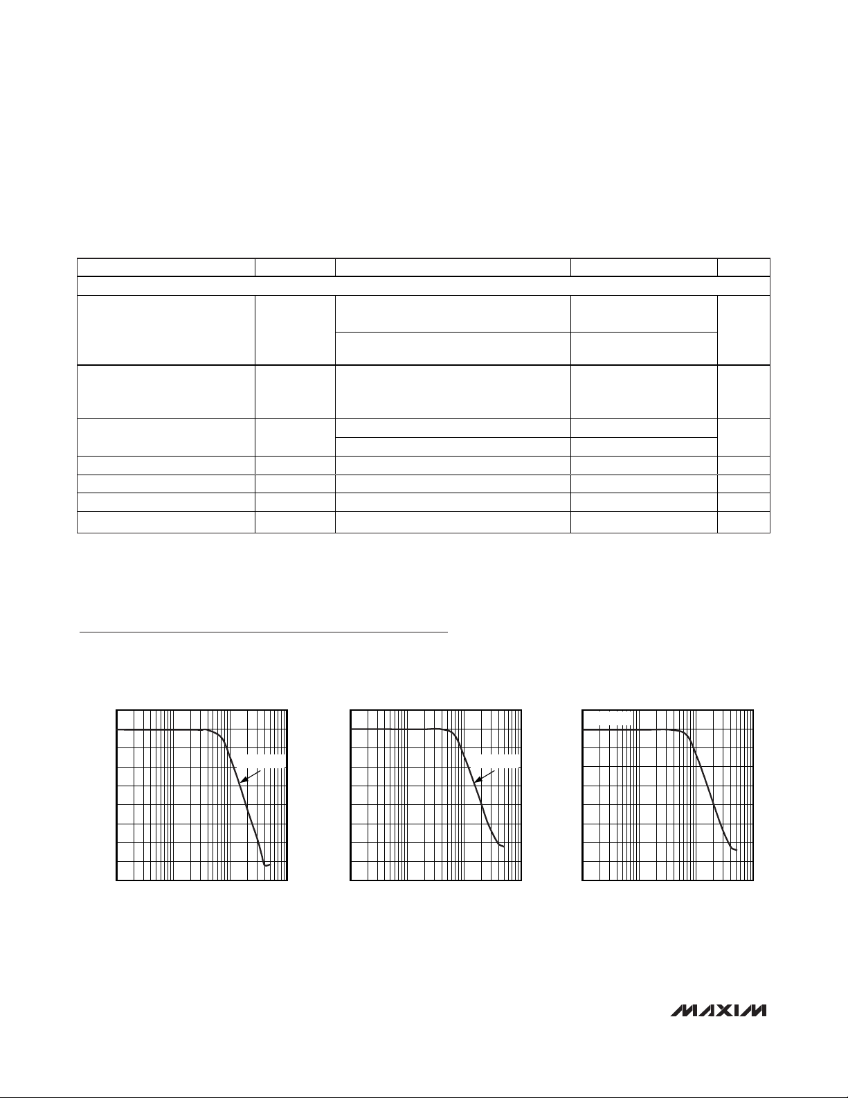
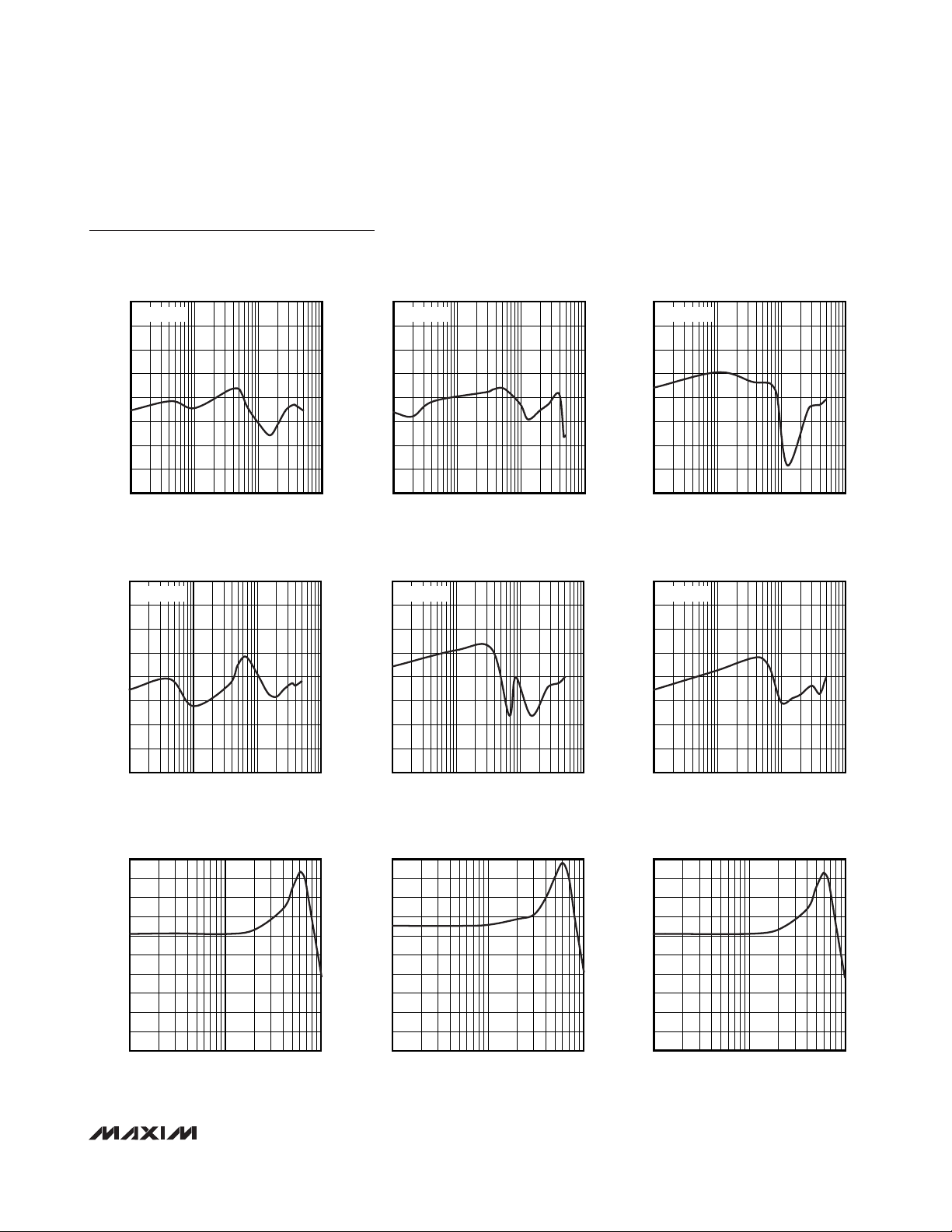
CHROMA LARGE-SIGNAL BANDWIDTH
MAX4079 toc01
FREQUENCY (MHz)
RESPONSE (dB)
101
-70
-60
-50
-40
-30
-20
-10
0
10
-80
0.1 100
VIN = 1V
P-P
LUMA LARGE-SIGNAL BANDWIDTH
MAX4079 toc02
FREQUENCY (MHz)
RESPONSE (dB)
101
-70
-60
-50
-40
-30
-20
-10
0
10
-80
0.1 100
VIN = 1V
P-P
CVBSOUT_ LARGE-SIGNAL BANDWIDTH
MAX4079 toc03
FREQUENCY (MHz)
RESPONSE (dB)
101
-70
-60
-50
-40
-30
-20
-10
0
10
-80
0.1 100
VIN = 1V
P-P
Typical Operating Characteristics
(V
VVID
= +5V, V
AUDV
= +12V, V
GVID
= V
GAUD
= 0V, R
IN_VIDEO
= 75Ω to GVID, C
IN_VIDEO
= 0.1µF, R
LOAD_VID
= 150Ω to GVID
,
C
OUT_AUDIO
= 10µF, R
LOAD_AUD
= 10kΩ to G
AUD
, R
REXT
= 10kΩ, C
BYPASS
= 1µF, TA= +25°C, unless otherwise noted.)
PARAMETER SYMBOL CONDITIONS MIN TYP MAX UNITS
AUDIO
Gain Flatness ΔA
Signal-to-Noise Ratio SNR
Total Harmonic Distortion
Plus Noise
Output Impedance Z
Power-Supply Rejection Ratio PSRR
Crosstalk X
Capacitive Load C
LOUT_, ROUT_, fIN = 20Hz to 20kHz,
AUD
0.5V
MONO, fIN = 20Hz to 20kHz, 0.5V
input
fIN = 1.0kHz, 0.5V
AUD
highpass filter at 20Hz, lowpass filter at
20kHz
THD+N
O,AUD
AUD,AC
TLK,AUD
L,AUD
fIN = 1.0kHz, 0.5V
f
f = 1kHz 0.2 Ω
f = 1kHz, V
f = 1kHz, 0.5V
No sustained oscillations 200 pF
input
RMS
= 1.0kHz, 1V
IN
RIPPLE
0.01
, CCIR weighing
RMS
RMS
0.01
85 dB
RMS
RMS
= 200mV
input 70 dB
RMS
P-P
0.005
0.003
60 dB
dB
%
MAX4079
Complete Audio/Video
Backend Solution
_______________________________________________________________________________________
5
Typical Operating Characteristics (continued)
(V
VVID
= +5V, V
AUDV
= +12V, V
GVID
= V
GAUD
= 0V, R
IN_VIDEO
= 75Ω to GVID, C
IN_VIDEO
= 0.1µF, R
LOAD_VID
= 150Ω to GVID
,
C
OUT_AUDIO
= 10µF, R
LOAD_AUD
= 10kΩ to G
AUD
, R
REXT
= 10kΩ, C
BYPASS
= 1µF, TA= +25°C, unless otherwise noted.)
VIDEO CROSSTALK (CVBSOUT_ TO YIN)
-40
VIN = 1V
-50
-60
-70
-80
RESPONSE (dB)
-90
-100
-110
-120
0.1 100
P-P
FREQUENCY (MHz)
VIDEO CROSSTALK (COUT TO YIN)
-40
VIN = 1V
-50
-60
-70
-80
RESPONSE (dB)
-90
-100
-110
-120
0.1 100
P-P
FREQUENCY (MHz)
101
101
MAX4079 toc04
MAX4079 toc07
VIDEO CROSSTALK (CVBSOUT_ TO CIN)
-40
VIN = 1V
-50
-60
-70
-80
RESPONSE (dB)
-90
-100
-110
-120
0.1 100
VIDEO CROSSTALK (YOUT TO CVBSIN)
-40
VIN = 1V
-50
-60
-70
-80
RESPONSE (dB)
-90
-100
-110
-120
0.1 100
P-P
FREQUENCY (MHz)
P-P
FREQUENCY (MHz)
VIDEO CROSSTALK (COUT TO CVBSIN)
-40
VIN = 1V
-50
MAX4079 toc05
-60
-70
-80
RESPONSE (dB)
-90
-100
-110
-120
101
0.1 100
P-P
FREQUENCY (MHz)
VIDEO CROSSTALK (YOUT TO CIN)
-40
VIN = 1V
-50
MAX4079 toc08
-60
-70
-80
RESPONSE (dB)
-90
-100
-110
-120
101
0.1 100
P-P
FREQUENCY (MHz)
MAX4079 toc06
101
MAX4079 toc09
101
100
90
80
70
60
50
DELAY (ns)
40
30
20
10
0
0.1 10
1
FREQUENCY (MHz)
CVBSOUT_ GROUP DELAY
MAX4079 toc10
100
CHROMA GROUP DELAY
90
80
70
60
50
DELAY (ns)
40
30
20
10
0
0.1 10
1
FREQUENCY (MHz)
MAX4079 toc11
100
YOUT GROUP DELAY
90
80
70
60
50
DELAY (ns)
40
30
20
10
0
0.1 10
1
FREQUENCY (MHz)
MAX4079 toc12

MAX4079
Complete Audio/Video
Backend Solution
6 _______________________________________________________________________________________
Typical Operating Characteristics (continued)
(V
VVID
= +5V, V
AUDV
= +12V, V
GVID
= V
GAUD
= 0V, R
IN_VIDEO
= 75Ω to GVID, C
IN_VIDEO
= 0.1µF, R
LOAD_VID
= 150Ω to GVID
,
C
OUT_AUDIO
= 10µF, R
LOAD_AUD
= 10kΩ to G
AUD
, R
REXT
= 10kΩ, C
BYPASS
= 1µF, TA= +25°C, unless otherwise noted.)
DIFFERENTIAL GAIN
MAX4079 toc13
DIFFERENTIAL PHASE (deg)
1324567
1324567
0.2
0.1
0
-0.1
-0.2
DIFFERENTIAL GAIN (%)
0.2
0.1
0
-0.1
-0.2
DIFFERENTIAL PHASE
AUDIO LARGE-SIGNAL BANDWIDTH
MAX4079 toc14
FREQUENCY (kHz)
RESPONSE (dB)
1010.1
2.8
2.9
3.0
3.1
3.2
3.3
2.7
0.01 100
MONO CHANNEL
VIN = 0.5V
RMS
AUDIO LARGE-SIGNAL BANDWIDTH
MAX4079 toc15
FREQUENCY (kHz)
RESPONSE (dB)
1010.1
5.5
6.0
6.5
7.0
5.0
0.01 100
RIGHT CHANNEL
VIN = 0.5V
RMS
AUDIO LARGE-SIGNAL BANDWIDTH
MAX4079 toc16
FREQUENCY (kHz)
RESPONSE (dB)
1010.1
5.5
6.0
6.5
7.0
5.0
0.01 100
LEFT CHANNEL
VIN = 0.5V
RMS
AUDIO CROSSTALK
MAX4079 toc17
FREQUENCY (kHz)
RESPONSE (dB)
1010.1
-110
-100
-90
-80
-70
-60
-50
-40
-120
0.01 100
LEFT TO RIGHT CHANNEL
RIGHT TO LEFT CHANNEL
VIN = 0.5V
RMS
TOTAL HARMONIC DISTORTION
PLUS NOISE RATIO (LEFT CHANNEL)
MAX4079 toc18
FREQUENCY (kHz)
THD+N (%)
1010.1
0.002
0.003
0.004
0.005
0.006
0.007
0.008
0.009
0.010
0.001
0.01 100
VIN = 1V
RMS
VIN = 0.5V
RMS

Typical Operating Characteristics (continued)
(V
VVID
= +5V, V
AUDV
= +12V, V
GVID
= V
GAUD
= 0V, R
IN_VIDEO
= 75Ω to GVID, C
IN_VIDEO
= 0.1µF, R
LOAD_VID
= 150Ω to GVID
,
C
OUT_AUDIO
= 10µF, R
LOAD_AUD
= 10kΩ to G
AUD
, R
REXT
= 10kΩ, C
BYPASS
= 1µF, TA= +25°C, unless otherwise noted.)
MAX4079
Complete Audio/Video
Backend Solution
_______________________________________________________________________________________
7
TOTAL HARMONIC DISTORTION
PLUS NOISE RATIO (RIGHT CHANNEL)
0.010
0.009
0.008
0.007
VIN = 0.5V
0.006
0.005
THD+N (%)
0.004
0.003
0.002
0.001
0.01 100
VIN = 1V
RMS
RMS
FREQUENCY (kHz)
3.5
VIN = 3.5V
3.2
2.9
2.6
INPUT CLAMP CURRENT (μA)
2.3
1010.1
MAX4079 toc19
VIDEO SUPPLY CURRENT (mA)
INPUT CLAMP CURRENT
vs. TEMPERATURE
CVBSIN
YIN
65
64
63
62
61
60
59
58
57
56
55
0 10203040506070
MAX4079 toc22
VIDEO SUPPLY CURRENT
vs. TEMPERATURE
TEMPERATURE (°C)
10,000
1000
INPUT CLAMP CURRENT (μA)
100
10
9.0
8.5
MAX4079 toc20
8.0
7.5
7.0
6.5
6.0
AUDIO SUPPLY CURRENT (mA)
5.5
5.0
02010 30 40 50 60 70
INPUT CLAMP CURRENT
vs. INPUT VOLTAGE
SOURCING
AUDIO SUPPLY CURRENT
vs. TEMPERATURE
TEMPERATURE (°C)
SINKING
YIN
CVBSIN
MAX4079 toc23
MAX4079 toc21
2.0
0 10203040506070
TEMPERATURE (°C)
OUTPUT BIAS VOLTAGE
vs. TEMPERATURE
1.3
1.2
1.1
1.0
0.9
OUTPUT BIAS VOLTAGE (V)
0.8
0.7
02010 30 40 50 60 70
YOUT
CVBSOUT_
TEMPERATURE (°C)
MAX4079 toc24
1
0 5.0
INPUT VOLTAGE (V)
OUTPUT BIAS VOLTAGE
vs. TEMPERATURE
2.5
2.3
2.1
1.9
OUTPUT BIAS VOLTAGE (V)
1.7
1.5
02010 30 40 50 60 70
COUT
TEMPERATURE (°C)
4.54.03.53.02.52.01.51.00.5
MAX4079 toc25

MAX4079
Detailed Description
The MAX4079 filters and buffers video (NTSC/PAL/DVB)
and stereo audio signals from the MPEG decoder of a
cable/satellite receiver, VCR/DVD player, or a TV to an
external load. The MAX4079 has luma-chroma (Y-C)
and composite (CVBS) video inputs with one Y-C and
two CVBS outputs. All video inputs are AC-coupled with
internal DC biasing on the chroma input and active
clamps for the luma and composite.
The MAX4079 video reconstruction filters have a 6MHz
cutoff frequency and 50dB attenuation at 27MHz. The
filters are matched, with flat group delay for standarddefinition video. The video gain is fixed at +6dB to drive
a 75Ω back-terminated load (150Ω) to unity gain. The
video outputs can be either DC- or AC-coupled and are
powered by a single +5V supply.
The MAX4079 audio amplifiers have differential inputs
for optimum performance, but can be used with singleended sources with external biasing. The audio channels have a fixed gain of +6dB and deliver 2.6V
RMS
output with a differential input of ±1.85V. The audio
amplifiers operate from a +9V to +12V single supply
and feature an internal bias generator. An on-chip
mixer also provides a mono output, with +3dB gain,
derived from the left and right audio channels.
Video
The video section of the MAX4079 implements DC
restore/biasing, amplification, and reconstruction filtering for the Y-C and CVBS input signals. All of the video
inputs are AC-coupled. DC restore is performed using
a sync tip clamp for both luma and composite video
channels. The chroma DC level input is biased at the
midlevel of the signal.
All video channels have a fixed gain of +6dB. The DC
level at the video outputs is controlled so that coupling
capacitors are not required.
All composite and luma video outputs are capable of
driving 2.4V
P-P
, and the chroma output is capable of
driving 1.8V
P-P
into 150Ω resistive load to ground. Up
to 35pF of load capacitance can be tolerated at each
video output without stability or slew-rate issues.
Complete Audio/Video
Backend Solution
8 _______________________________________________________________________________________
Pin Description
PIN NAME FUNCTION
1 REXT External Filter Resistor. Bypass with a 10kΩ ±1% resistor and a 0.1µF capacitor to GVID.
2, 24 VVID Video Power-Supply Input
3 CVBSIN Composite Video Input
4, 21 GVID Video Ground
5 YIN Luma Input
6 CBYPASS Audio LDO Regulator Bypass Capacitor. Bypass with a1µF capacitor to GAUD.
7 CIN Chroma Input
8 AUDV Audio Power-Supply Input
9 LINP Left-Channel Audio Positive Input
10 LINN Left-Channel Audio Negative Input
11 RINN Right-Channel Audio Negative Input
12 RINP Right-Channel Audio Positive Input
13 ROUT2 Right-Channel Audio Output 2
14 ROUT1 Right-Channel Audio Output 1
15 GAUD Audio Ground
16 MONO Mono Audio Output
17 LOUT2 Left-Channel Audio Output 2
18 LOUT1 Left-Channel Audio Output 1
19 COUT Chroma Video Output
20 YOUT Luma Video Output
22 CVBSOUT1 Composite Video Output 1
23 CVBSOUT2 Composite Video Output 2

All video inputs are stable with up to 150Ω source resistance. For higher values, consult Maxim applications.
Video Reconstruction Filter
The MAX4079 reconstruction filters are 4th-order
Butterworth filters that provide a cutoff frequency of
6MHz and flat group delay response up to 4.5MHz. The
stopband offers 26dB of attenuation at 13.5MHz and
50dB at 27MHz.
Audio
The audio section of the MAX4079 is a stereo amplifier
with one differential input and two single-ended outputs
for each channel (left and right). A mono output is provided by summing the two channels of the stereo signal
together. The stereo channels have a +6dB typical
gain, while the mono has a +3dB gain.
The audio inputs can be DC-coupled, eliminating spaceconsuming coupling capacitors. Each of the five outputs
can deliver 2.6V
RMS
into an AC-coupled 10kΩ load.
Applications Information
Audio DAC Interfacing
Differential Audio DAC
The MAX4079 accepts differential audio signals. Figure
1 shows a typical configuration for connecting the
device to an audio DAC with differential outputs. Figure
2 shows the reconstruction filters that can be used for
the differential audio inputs. Carefully select resistors
and capacitors to attenuate out-of-band noise and mini-
mize the effect on the gain. The common-mode voltage
for these signals is typically 2.5V.
Single-Ended Audio DAC
The MAX4079 can also be configured for single-ended
inputs. Figure 3 shows how to connect an audio DAC with
single-ended outputs to the MAX4079. Figure 4 shows
how reconstruction filters can be used for single-ended
audio inputs. Choose these values to minimize the
effect on gain.
If the single-ended audio DAC does not include a common-mode voltage output, create a bias point with wellmatched resistors and couple the audio signal to the
positive differential input (see Figure 5). The bias point
can also be created using a resistor-divider network
from the video supply voltage. Note that the tolerance of
the resistors will affect the common-mode and powersupply rejection ratios. Tighter tolerances improve the performance of CMRR and PSRR, e.g., 1% resistors will not
give any better than 40dB of CMRR and PSRR, whereas
0.1% resistors could improve the number to 60dB.
Power Supplies and Bypassing
The MAX4079 features single +5V (video) and +12V
(audio) supply operation, and requires no negative
supply. Connect the VVID pins together and bypass to
GVID with 0.01µF, 0.1µF, and 4.7µF capacitors in parallel. Bypass the AUDV to GAUD with 0.1µF, 1µF, and
47µF capacitors in parallel. Bypass CBYPASS to GAUD
with a 1µF capacitor (see the
Typical Operating Circuit
).
MAX4079
Complete Audio/Video
Backend Solution
_______________________________________________________________________________________ 9
Figure 1. Differential Audio Inputs
Figure 2. Filtering Differential Audio Inputs
+5V
A
OUTL+
A
OUTL-
AUDIO
DAC
A
OUTR+
A
OUTR-
LINP
LINN
RINP
RINN
LEFT AUDIO
CHANNEL
RIGHT AUDIO
CHANNEL
MAX4079
A
OUTL+
A
OUTL-
R1
C1
R1
R2
R2
LINP
LINN
C2
C2
MAX4079

MAX4079
Complete Audio/Video
Backend Solution
10 ______________________________________________________________________________________
Figure 3. Single-Ended Audio Inputs
Figure 4. Filtering Single-Ended Audio Inputs
Figure 5. Biasing Single-Ended Audio Inputs
Figure 6. Vertical Sync Interval
Layout and Grounding
For optimal performance, stitch ground vias between the
narrow adjacent signal traces to minimize crosstalk.
Avoid running video traces parallel to high-speed data
lines. The MAX4079 provides separate ground connections
for video and audio supplies. For best performance use
separate ground planes for each of the ground returns,
and connect all ground planes together at a single point.
Refer to the MAX4079 Evaluation Kit for a proven circuit
board layout example.
+5V
LINP
LINN
~2.5V
RINP
RINN
AUDIO
DAC
A
A
OUTL
V
CM
OUTR
V
BIAS
LEFT AUDIO
CHANNEL
RIGHT AUDIO
CHANNEL
MAX4079
A
OUTL
V
CM
R1
C1
R1
LINP
LINN
MAX4079
R
A
OUTL
R
R
A
OUTR
R
R
LINP
LINN
R
V
BIAS
R
RINP
RINN
R
LEFT AUDIO
CHANNEL
MAX4079
RIGHT AUDIO
CHANNEL
INPUT
OUTPUT
40μs/div

MAX4079
Complete Audio/Video
Backend Solution
______________________________________________________________________________________ 11
Typical Operating Circuit
+5V VIDEO SUPPLY
4.7μF
YIN
0.1μF
RINN
LINN
0.1μF
RINP
LINP
0.01μF
75Ω
75Ω
75Ω
10kΩ
0.1μF
0.1μF
0.1μF
VVID
VVID
GVID
GVID
YIN
CINCIN
CVBSINCVBSIN
RINP
RINN
LINP
LINN
REXT
MAX4079
AUDV
GAUD
YOUT
COUT
CVBSOUT1
CVBSOUT2
ROUT1
ROUT2
MONO
LOUT1
LOUT2
CBYPASS
10μF
+12V AUDIO SUPPLY
0.1μF
75Ω
75Ω
75Ω
75Ω
10μF
10kΩ
10μF
10kΩ
330μF
47μF
*OPTIONAL CAPACITORS
(TYPICAL VALUES SHOWN)
Z
Z
Z
Z
10kΩ
10μF
10kΩ
= 75Ω
0
= 75Ω
0
= 75Ω
0
= 75Ω
0
10kΩ
75Ω
75Ω
1μF
330μF
330μF
330μF
10μF
75Ω
75Ω
1μF

MAX4079
Complete Audio/Video
Backend Solution
12 ______________________________________________________________________________________
Pin Configuration
Chip Information
PROCESS: BiCMOS
TOP VIEW
REXT
VVID
CVBSIN
YIN
CBYPASS
CIN
LINP
LINN
RINN
+
1
2
3
4
MAX4079
5
6
7
8
9
10
11
12
TSSOP
24
23
22
21
20
19
18
17
16
15
14
13
VVID
CVBSOUT2
CVBSOUT1
GVIDGVID
YOUT
COUT
LOUT1
LOUT2AUDV
MONO
GAUD
ROUT1
ROUT2RINP

MAX4079
Complete Audio/Video
Backend Solution
______________________________________________________________________________________ 13
MAX4079
PACKAGE TYPE PACKAGE CODE DOCUMENT NO.
24 TSSOP U24+1
21-0066
Package Information
For the latest package outline information and land patterns, go to www.maxim-ic.com/packages.
TSSOP4.40mm.EPS

MAX4079
Complete Audio/Video
Backend Solution
14 ______________________________________________________________________________________
Package Information (continued)
For the latest package outline information and land patterns, go to www.maxim-ic.com/packages.
N
1
TOP VIEW
e
FRONT VIEW
MAX
0.104
0.012
0.019
0.013
0.299
0.050
MAX
0.5120.496D
MILLIMETERS
MAX
MIN
2.65
2.35
0.30
0.10
0.49
0.35
0.23
0.32
7.40 7.60
0.40 1.27
MILLIMETERS
MAX
MIN
12.60 13.00
SOICW.EPS
N MS013
20 AC
INCHES
MIN
DIM
0.093A
0.004
A1
0.014
B
0.009
C
H
E
D
A
B
A1
C
L
e 0.050 1.27
0.291
E
H 0.4190.394 10.00 10.65
0.016L
VARIATIONS:
INCHES
MINDIM
0.398 0.413 AA10.5010.10 16
D
0.447 0.463 AB11.7511.35 18
D
D 0.6140.598 15.20 2415.60 AD
D 0.7130.697 17.70 2818.10 AE
0∞-8∞
SIDE VIEW
PROPRIETARY INFORMATION
TITLE:
PACKAGE OUTLINE, .300" SOIC
21-0042
REV.DOCUMENT CONTROL NO.APPROVAL
1
B
1

MAX4079
Complete Audio/Video
Backend Solution
Heaney
Maxim cannot assume responsibility for use of any circuitry other than circuitry entirely embodied in a Maxim product. No circuit patent licenses are
implied. Maxim reserves the right to change the circuitry and specifications without notice at any time.
Maxim Integrated Products, 120 San Gabriel Drive, Sunnyvale, CA 94086 408-737-7600 ____________________
15
© 2009 Maxim Integrated Products Maxim is a registered trademark of Maxim Integrated Products, Inc.
Revision History
REVISION
NUMBER
0 8/05 Initial release —
1 3/09 Changes to remove SO package, style edits 1–7, 12, 13, 14
REVISION
DATE
DESCRIPTION
CHANGED
PAGES
 Loading...