

Page 1
General Description
The MAX4063 is a differential-input microphone preamplifier optimized for high-performance, portable applications. The device features two selectable inputs,
differential outputs, adjustable gain, an integrated lownoise bias source, and a low-power shutdown mode.
Two input paths provide both differential and singleended microphone sensing. The high-noise rejection of
the differential input is ideally suited to an internal microphone where system noise and long-run PC board traces
can degrade low-level signals. The single-ended input
provides a simple connection to an external microphone.
The differential and single-ended inputs have independent, adjustable gains that are set with a single external
resistor. Differential outputs provide a full-scale signal of
up to 6V
P-P
from a single 3V supply, optimizing the
dynamic range of the amplified signal. A complete shutdown mode reduces the supply current to only 0.3µA
and disables the microphone bias for the ultimate in
power savings.
The MAX4063 operates from 2.4V to 5.5V and is specified
over the extended -40°C to +85°C operating temperature
range. The MAX4063 is available in both 16-pin thin QFN
(4mm x 4mm x 0.8mm) and 14-pin TSSOP packages.
Applications
Features
♦ 2.4V to 5.5V Single-Supply Operation
♦ Differential Inputs and Outputs
♦ Adjustable Gain
♦ High 95dB PSRR
♦ High 79dB CMRR
♦ Low-Noise, Integrated Microphone Bias
♦ 750µA Supply Current
♦ 0.3µA Shutdown Current
♦ ±4kV ESD Protection (AUX_IN)
♦ THD+N: 0.05% at 1kHz
♦ Available in Space-Saving Packages
14-Pin TSSOP
16-Pin Thin QFN (4mm x 4mm x 0.8mm)
MAX4063
Differential Microphone Preamplifier with
Internal Bias and Complete Shutdown
________________________________________________________________ Maxim Integrated Products 1
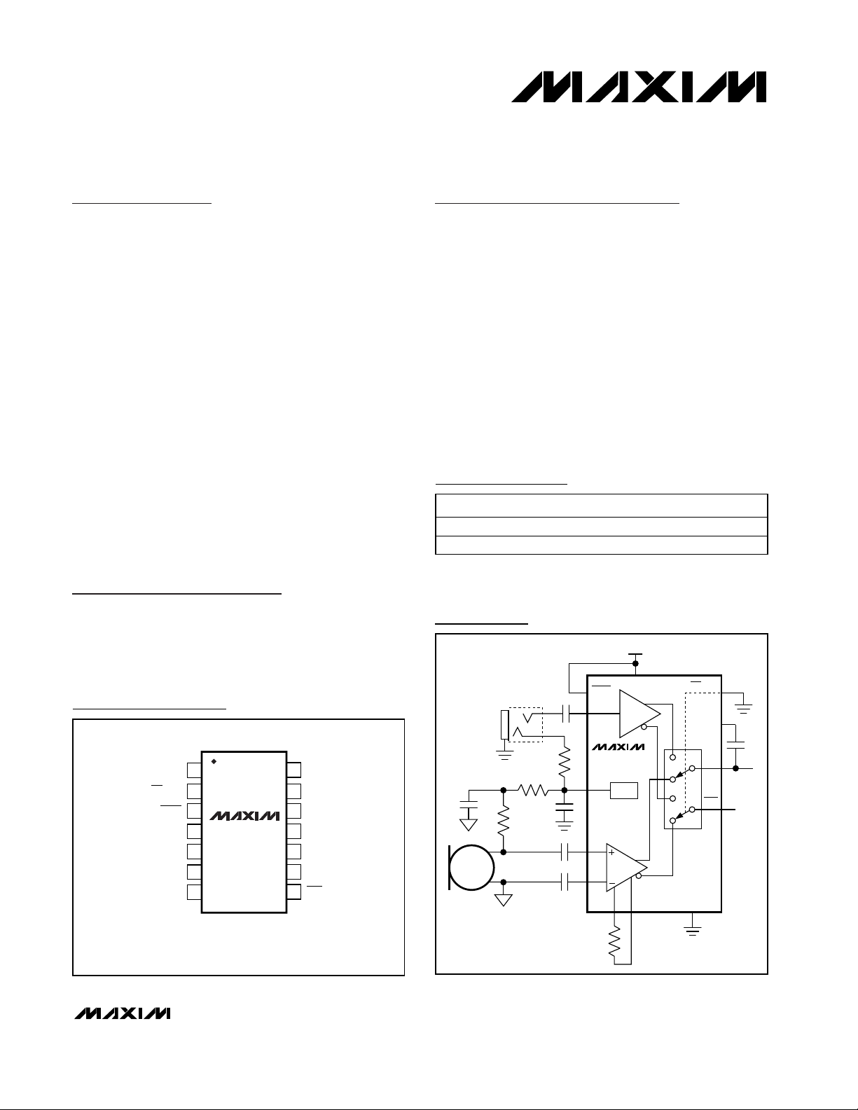
Typical Operating Circuit
Ordering Information
19-2753; Rev 0; 1/03
For pricing, delivery, and ordering information, please contact Maxim/Dallas Direct! at
1-888-629-4642, or visit Maxim’s website at www.maxim-ic.com.
Notebook Audio Systems
Tablet PCs
PDA Audio Systems
Signal Conditioning
Pin Configurations
Pin Configurations continued at end of data sheet.
*Future product—contact factory for availability.
**EP = Exposed paddle.
PART TEMP RANGE PIN-PACKAGE
MAX4063ETE* -40°C to +85°C 16 Thin QFN-EP**
MAX4063EUD -40°C to +85°C 14 TSSOP
2.4V TO 5.5V
6
V
SHDN
AUX_IN
CC
INT/AUX
ADJ
3
12
2
7
1
G2
2
INT/AUX
3
SHDN
4
MAX4063
BIAS
5
V
6
CC
7
TSSOP
14
G1
13
N.C.
12
AUX_IN
11
GNDOUT
IN-
10
9
IN+
OUTADJ
8
5
9
10
MAX4063
BIAS
IN+
IN-
R
G
V
BIAS
G1 G2
14
1
OUT
OUT 8
GND
11
4
Page 2
MAX4063
Differential Microphone Preamplifier with
Internal Bias and Complete Shutdown
2 _______________________________________________________________________________________
ABSOLUTE MAXIMUM RATINGS
ELECTRICAL CHARACTERISTICS
(VCC= 3V, GND = 0V, SHDN = V
CC,
INT/AUX = 0V, RG= 11.11kΩ, RL= 100kΩ to 1.5V, R
BIAS
= ∞, V
OUT
is measured between OUT
and OUT. T
A
= T
MIN
to T
MAX
, unless otherwise noted. Typical values are at TA= +25°C.) (Notes 1 and 2)
Stresses beyond those listed under “Absolute Maximum Ratings” may cause permanent damage to the device. These are stress ratings only, and functional
operation of the device at these or any other conditions beyond those indicated in the operational sections of the specifications is not implied. Exposure to
absolute maximum rating conditions for extended periods may affect device reliability.
Supply Voltage (VCCto GND). .................................-0.3V to +6V
Any Other Pin to GND ................................-0.3V to (V
CC
+ 0.3V)
Duration of Short Circuit to GND or V
CC
....................Continuous
Continuous Input Current (any pin) ................................ ±10mA
Continuous Power Dissipation (T
A
= +70°C)
14-Pin TSSOP (derate 9.1mW/°C above +70°C) ..........667mW
16-Pin Thin QFN (derate 16.9mW/°C above +70°C) ..1349mW
Operating Temperature Range ...........................-40°C to +85°C
Storage Temperature Range .............................-65°C to +150°C
Lead Temperature (soldering, 10s) .................................+300°C
Supply Voltage Range V
Supply Current I
Output Common-Mode Voltage V
Slew Rate SR AV = 20V/V ±1 V/µs
Supply Current in Shutdown I
Output Short-Circuit Current I
DIFFERENTIAL INPUT (INT/AUX = 0V)
Input Offset Voltage V
Common-Mode Input Voltage Range V
Maximum Differential Input Voltage V
Small-Signal Bandwidth BW
Input Resistance R
Input Resistance Match R
Input Noise-Voltage Density e
RMS Output Noise Voltage V
Total Harmonic Distortion Plus Noise THD+N
Common-Mode Rejection Ratio CMRR VCM = 500mV
PARAMETER SYMBOL CONDITIONS MIN TYP MAX UNITS
Inferred from PSRR test 2.4 5.5 V
CC
CC
OCM
SHDNV SHDN
SC
OS
CM
DIFFMAXAV
-3dB
IN
MATCH
n
NRMSAV
VDIFF
= 0V 0.001 1 µA
To GND 30
To V
CC
TA = +25°C ±1mV
Inferred from CMRR test 1 2 V
= 2V/V 1 V
Either differential input 100 kΩ
AV = 20V/V, f = 1kHz 70
AV = 200V/V, f = 1kHz 12
= 20V/V, BW = 22Hz to 22kHz 225 µV
A
= 20V/V, f = 1kHz, V
V
BW = 22Hz to 22kHz
1V < VCM < 2V,
V
= 0.7V
OUT
TA = +25°C95
TA = T
V
CC
- T
MIN
= 5V ±100mV, f = 1kHz 86
= 0.7V
OUT
RG = open 2
RMS
MAX
RG = 11.11kΩ 19.2 20 20.8Differential Gain A
RG = 1.01kΩ 200
, f = 1kHz 70 dB
P-P
RMS
,
0.75 1.1 mA
1.25 1.5 1.75 V
30
600 kHz
1%
0.05 %
85Power-Supply Rejection Ratio PSRR
mA
nV/√Hz
RMS
V/V
dB
Page 3
MAX4063
Differential Microphone Preamplifier with
Internal Bias and Complete Shutdown
_______________________________________________________________________________________ 3
ELECTRICAL CHARACTERISTICS (continued)
(VCC= 3V, GND = 0V, SHDN = V
CC,
INT/AUX = 0V, RG= 11.11kΩ, RL= 100kΩ to 1.5V, R
BIAS
= ∞, V
OUT
is measured between OUT
and OUT. T
A
= T
MIN
to T
MAX
, unless otherwise noted. Typical values are at TA= +25°C.) (Notes 1 and 2)
Note 1: All specifications are 100% tested at TA= +25°C. Specification limits over temperature (TA= T
MIN
to T
MAX
) are guaranteed
by design, not production tested.
Note 2: MAX4063 requires a 1µF capacitor from BIAS to ground and a 10pF capacitor from ADJ to OUT.
AUXILIARY INPUT (INT/AUX = VCC)
Small-Signal Bandwidth BW
Input Resistance R
Input Noise-Voltage Density e
RMS Output Noise Voltage V
Total Harmonic Distortion Plus Noise THD+N f = 1kHz, BW = 22Hz to 22kHz 0.007 %
Power-Supply Rejection Ratio PSRR
Voltage Gain A
BIAS OUTPUT
Output Voltage V
Output Resistance R
Output Noise Voltage V
Power-Supply Rejection Ratio PSRR
DIGITAL INPUTS (SHDN and INT/AUX)
Input Leakage Current I
Input Voltage High V
Input Voltage Low V
Shutdown Enable Time t
Shutdown Disable Time t
PARAMETER SYMBOL CONDITIONS MIN TYP MAX UNITS
-3dB
IN
f = 1kHz 200 nV/√Hz
n
NRMS
VAUXVOUT
OUTIBIAS
NRMSIBIAS
OFF
BW = 22Hz to 22kHz 620 µV
TA = +25°C 80 100
T
= T
A
OUTIBIAS
I
BIAS
I
BIAS
f = 1kHz
VIN = 0V or V
IN
INH
INL
ON
- T
MIN
MAX
= 0.7V
RMS
= 0.5mA to GND 2 2.2 V
= 0.5mA to GND 16 30 Ω
= 0.5mA to GND, BW = 22Hz to 22kHz 20 µV
= 0.5mA to GND, VCC = 2.4V to 5.5V 60 74
= 0.5mA, VCC = 3V + 100mV
CC
P-P
,
-19.5 -20 -20.5 V/V
0.7 ✕ V
230 kHz
100 kΩ
72
71
CC
0.3 ✕ V
10 µs
10 µs
±1µA
CC
RMS
dB
RMS
dB
V
V
Page 4
MAX4063
Differential Microphone Preamplifier with
Internal Bias and Complete Shutdown
4 _______________________________________________________________________________________
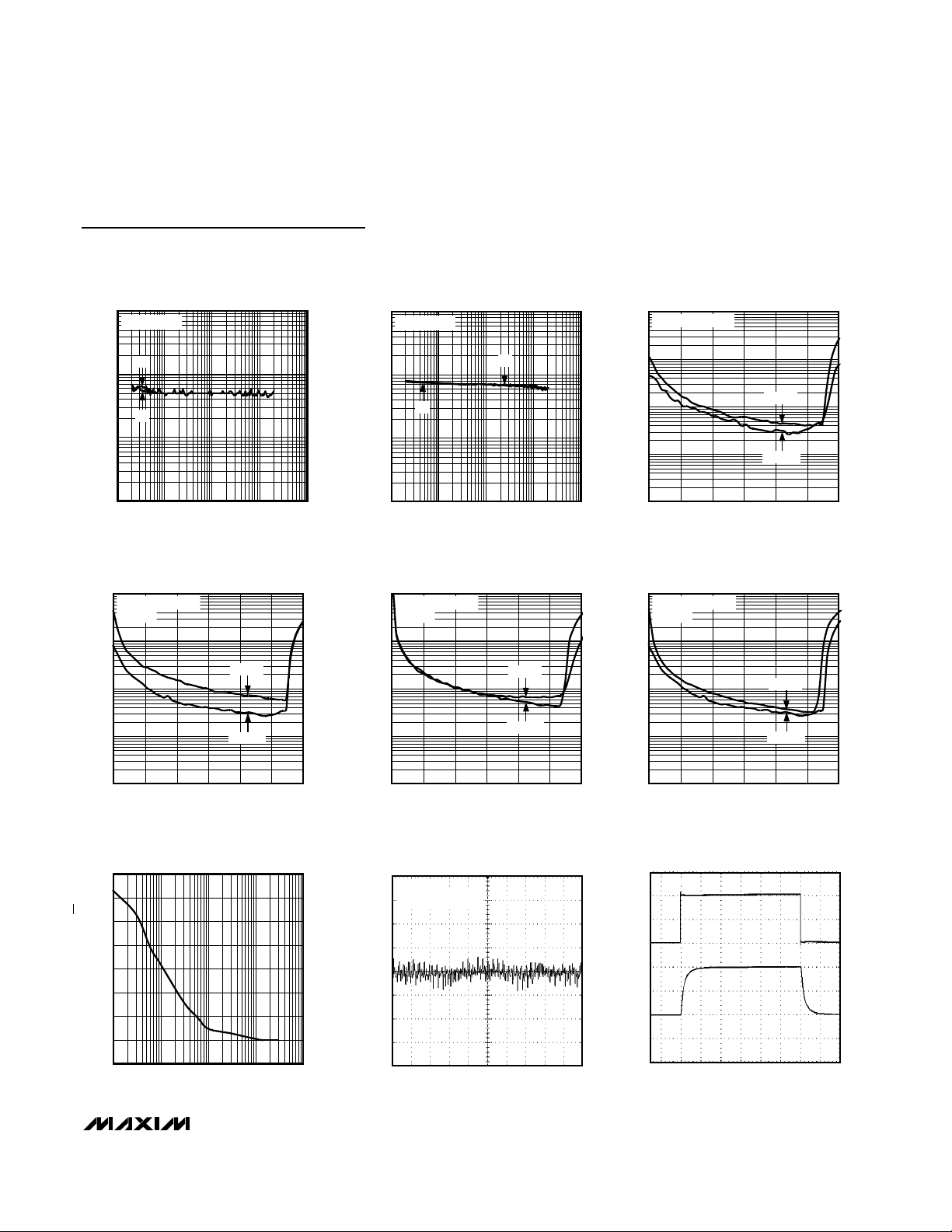
Typical Operating Characteristics
(VCC= 3V, AV= 20V/V, RL≥ 100kΩ to 1.5V, SHDN = VCC, V
OUT
is measured between OUT and OUT. TA= +25°C, unless otherwise
noted.)
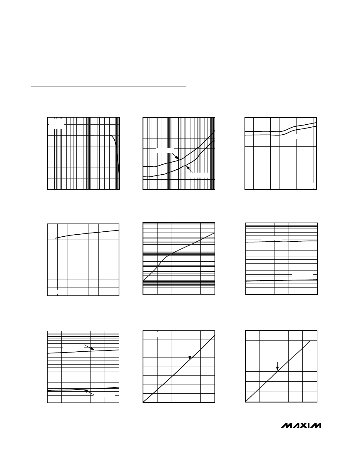
GAIN vs. FREQUENCY
(NO LOAD)
VCC = 5V
9
= 2V/V
A
V
6
3
0
GAIN (dB)
-3
-6
-9
10 1M
FREQUENCY (Hz)
SUPPLY CURRENT vs. SUPPLY VOLTAGE
0.9
0.8
0.7
0.6
0.5
0.4
0.3
SUPPLY CURRENT (mA)
0.2
0.1
NO LOAD
0
2.0 5.5
SUPPLY VOLTAGE (V)
100k10k1k100
5.04.53.5 4.03.02.5
0
-20
MAX4063 toc01
-40
-60
PSRR (dB)
-80
-100
-120
-140
100
10
MAX4063 toc04
1
0.1
0.01
SHUTDOWN SUPPLY CURRENT (nA)
0.001
POWER-SUPPLY REJECTION RATIO
vs. FREQUENCY (DIFF INPUT)
10 1M
SHUTDOWN SUPPLY CURRENT
-40 85
SUPPLY CURRENT vs. TEMPERATURE
1.0
VCC = 5V
0
-40
AV = 20V/V
FREQUENCY (Hz)
AV = 200V/V
100k10k1k100
MAX4063 toc02
SUPPLY CURRENT (mA)
0.8
0.6
0.4
0.2
vs. TEMPERATURE
1000
MAX4063 toc05
100
(mV)
OH
V
10
603510-15
TEMPERATURE (°C)
1
-40 85
VCC = 3V
TEMPERATURE (°C)
VOH vs. TEMPERATURE
I
= 2.5mA
LOAD
I
LOAD
TEMPERATURE (°C)
MAX4063 toc03
NO LOAD
80655035205-10-25
MAX4063 toc06
= 50µA
603510-15
1000
VOL vs. TEMPERATURE
I
= 2.5mA
LOAD
100
(mV)
OL
V
10
I
1
-40 85
TEMPERATURE (°C)
LOAD
= 50µA
603510-15
MAX4063 toc07
VOH vs. LOAD CURRENT
(mV)
OL
V
350
300
250
200
150
100
50
0
400
VOH = V
- V
CC
350
300
250
(mV)
200
OH
V
150
100
50
0
05
OUT
MAX4063 toc08
VCC = 3V
4321
LOAD CURRENT (mA)
VOL vs. LOAD CURRENT
VCC = 3V
LOAD CURRENT (mA)
MAX4063 toc09
432105
Page 5
MAX4063
Differential Microphone Preamplifier with
Internal Bias and Complete Shutdown
_______________________________________________________________________________________ 5
Typical Operating Characteristics (continued)
(VCC= 3V, AV= 20V/V, RL≥ 100kΩ to 1.5V, SHDN = VCC, V
OUT
is measured between OUT and OUT. TA= +25°C, unless otherwise
noted.)
10 1k100 10k 100k
TOTAL HARMONIC DISTORTION PLUS
NOISE vs. FREQUENCY (DIFF INPUT)
MAX4063 toc10
FREQUENCY (Hz)
THD+N (%)
1
0.001
0.01
0.1
V
OUT
= 4.5V
P-P
5V
3V
10 1k100 10k 100k
TOTAL HARMONIC DISTORTION PLUS
NOISE vs. FREQUENCY (AUX INPUT)
MAX4063 toc11
FREQUENCY (Hz)
THD+N (%)
1
0.001
0.01
0.1
V
OUT
= 4.5V
P-P
5V
3V
10
0.001
02146
TOTAL HARMONIC DISTORTION PLUS NOISE
vs. OUTPUT AMPLITUDE (DIFF INPUT)
0.01
0.1
1
MAX4063 toc12
OUTPUT VOLTAGE (V
P-P
)
THD+N (%)
35
BW = 22Hz TO 22kHz
f = 1kHz
f = 10kHz
10
0.001
02146
TOTAL HARMONIC DISTORTION PLUS NOISE
vs. OUTPUT AMPLITUDE (DIFF INPUT)
0.01
0.1
1
MAX4063 toc13
OUTPUT VOLTAGE (V
P-P
)
THD+N (%)
35
BW = 22Hz TO 22kHz
V
CC
= 5V
f = 1kHz
f = 10kHz
10
0.001
02146
TOTAL HARMONIC DISTORTION PLUS NOISE
vs. OUTPUT AMPLITUDE (AUX INPUT)
0.01
0.1
1
MAX4063 toc14
OUTPUT VOLTAGE (V
P-P
)
THD+N (%)
35
BW = 22Hz TO 22kHz
V
CC
= 5V
f = 1kHz
f = 10kHz
10
0.001
02146
TOTAL HARMONIC DISTORTION PLUS NOISE
vs. OUTPUT AMPLITUDE (AUX INPUT)
0.01
0.1
1
MAX4063 toc15
OUTPUT VOLTAGE (V
P-P
)
THD+N (%)
35
BW = 22Hz TO 22kHz
V
CC
= 5V
f = 1kHz
f = 10kHz
MIC BIAS OUTPUT NOISE
MAX4063 toc17
100ms/div
20µV/div
VCC = 5V
BW = 22Hz TO 22kHz
SMALL-SIGNAL TRANSIENT RESPONSE
FOR DIFF INPUT
MAX4063 toc18
10µs/div
DIFF
INPUT
5mV/div
DIFF
OUTPUT
50mV/div
MAX4063 toc16
FREQUENCY (Hz)
INPUT-REFERRED NOISE (nV/√Hz)
10k1k100
50
100
150
200
250
300
350
400
0
10 100k
INPUT-REFERRED NOISE
vs. FREQUENCY (DIFF INPUT)
Page 6

MAX4063
Differential Microphone Preamplifier with
Internal Bias and Complete Shutdown
6 _______________________________________________________________________________________
Typical Operating Characteristics (continued)
(VCC= 3V, AV= 20V/V, RL≥ 100kΩ to 1.5V, SHDN = VCC, V
OUT
is measured between OUT and OUT. TA= +25°C, unless otherwise
noted.)
SMALL-SIGNAL TRANSIENT RESPONSE
FOR AUX INPUT
MAX4063 toc19
S/E
INPUT
5mV/div
DIFF
OUTPUT
100mV/div
LARGE-SIGNAL TRANSIENT RESPONSE
FOR DIFF INPUT
MAX4063 toc20
DIFF
INPUT
100mV/div
DIFF
OUTPUT
2V/div
10µs/div
LARGE-SIGNAL TRANSIENT RESPONSE
FOR AUX INPUT
10µs/div
MAX4063 toc21
S/E
INPUT
100mV/div
DIFF
OUTPUT
2V/div
10µs/div
OUTPUT OVERDRIVEN
10µs/div
MAX4063 toc22
DIFF
INPUT
500mV/div
DIFF
OUTPUT
2V/div
Page 7

MAX4063
Differential Microphone Preamplifier with
Internal Bias and Complete Shutdown
_______________________________________________________________________________________ 7
Detailed Description
The MAX4063 is a differential microphone preamplifier providing high-quality amplification, optimized
for use in computer and mobile applications. This device
features adjustable gain, very high power-supply rejection (95dB), and common-mode rejection (79dB), making
it ideal for low-noise applications. The MAX4063 provides
a differential input stage, making the device particularly
effective when layout constraints force the microphone
amplifier to be physically remote from the ECM microphone.
The MAX4063 is capable of switching its output
between the differential input and an inverting singleended input. INT/AUX selects either the differential
input or single-ended auxiliary input. In addition, the
MAX4063 has an integrated microphone bias source,
simplifying system design and eliminating the need for
external components. The MAX4063 has a complementary output allowing CODECs and other devices with
differential inputs to be optimally driven (see Functional
Diagram). The MAX4063 includes a 0.3µA shutdown
mode for ultimate power savings. The differential gain
of the MAX4063 is set with a single resistor connected
between the G1 and G2 pins. The MAX4063 has an
internal default gain of 20V/V on the AUX_IN input. The
AUX_IN gain can be increased with a single external
resistor (see the Differential-Gain Adjustment and
Auxiliary Input-Gain Adjustment sections).
Differential Input
The main microphone amplifier is a low-noise, differential input structure. This is an almost essential element
when faced with amplification of low-amplitude analog
signals in digitally intense environments such as note-
Pin Description
PIN
TSSOP QFN
115 G2
216INT/AUX
31SHDN
4 2 OUT Amplifier Output. OUT is high impedance when in shutdown mode.
5 3 BIAS
64VCCPower Supply. Bypass the VCC to GND with a 0.1µF capacitor.
7 5 ADJ
87OUT Complementary Amplifier Output. OUT is high impedance in shutdown mode.
9 9 IN+ Noninverting Differential Amplifier Input. AC-couple the audio signal into IN+.
10 10 IN- Inverting Differential Amplifier Input. AC-couple the audio signal into IN-.
11 11 GND Ground
12 12 AUX_IN Single-Ended Input for Auxiliary Microphone. AC-couple the audio signal into AUX_IN.
13 6, 8, 14 N.C. No Connection. Not internally connected.
14 13 G1
NAME FUNCTION
Gain-Selectable Input. Connect an external resistor between G1 and G2 to set the gain for
the differential amplifier (see Adjustable Differential Gain-Setting section).
Internal (Differential) or Auxiliary (Single-Ended) Input Select. Drive INT/AUX low to select
differential in or high to select auxiliary in.
Shutdown Input. Drive SHDN high for normal operation. Drive SHDN low for shutdown
mode.
External Electret Microphone Capsule Bias Output. Bypass BIAS with a 1µF capacitor to
ground.
Adjustable Gain Select for AUX_IN (see Auxiliary Input-Gain Adjustment section). Connect
a 10pF capacitor between OUT and ADJ.
Gain-Selectable Input. Connect an external resistor between G1 and G2 to set the gain for
the differential amplifier.
Page 8

MAX4063
Differential Microphone Preamplifier with
Internal Bias and Complete Shutdown
8 _______________________________________________________________________________________
book PCs or PDAs. Used correctly, the advantages
over a single-ended solution are:
• Better power-supply noise rejection.
• Less degradation from noise in PC board ground
planes.
• The microphone and preamplifier may be placed
physically further apart, easing PC board layout
restrictions.
Differential-Gain Adjustment
The MAX4063 allows the user to alter the differential
gain to optimize the signal-to-noise ratio (SNR) of their
system. The gain is set by a single external resistor
(RG) connected between the G1 and G2 pins:
where AVis the required voltage gain.
Hence, an 11.11kΩ resistor yields a gain of 20V/V, or
26dB. Leaving the pins unconnected results in a gain of
2V/V. Gain is defined as:
For differential out:
The resistor can be either fixed or variable, allowing the
use of a digitally controlled potentiometer to alter the
gain under software control.
Auxiliary Input-Gain Adjustment
The MAX4063 provides an option to increase the
AUX_IN (see Figure 3). To increase the gain, connect
resistor R
ADJ
between the ADJ and AUX_IN pins. R
ADJ
is
calculated from the following formula:
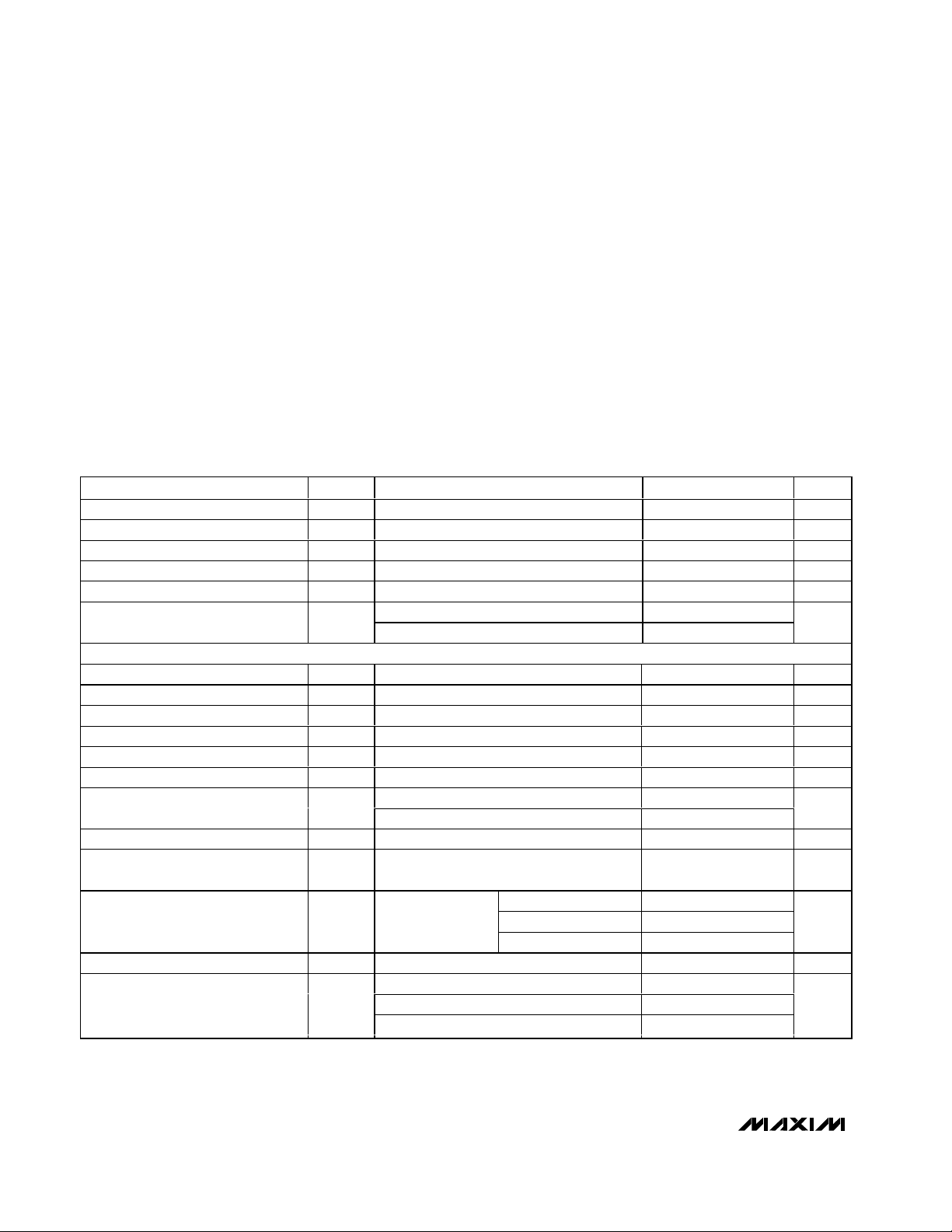
Functional Diagram
BIAS
BIAS
R
2.4V TO 5.5V
6
V
CC
MAX4063
AUX_IN
12
G1
14
G
1
G2
9
IN+
10
IN-
V
CC
3
SHDN
SHDN
V
GND
11
BIAS
ADJ
OUT
2INT/AUX
7
4
8OUT
BIAS
5
V
−−V
VD
OUT OUT
=
V
IN+ IN-
V
A
Ω
200k
R
=
G
−
2
A
VD
R
=
ADJ
Ω
AV
2M
AUX
()to increase the gain
−
20
Page 9

MAX4063
Differential Microphone Preamplifier with
Internal Bias and Complete Shutdown
_______________________________________________________________________________________ 9
where:
R
ADJ
is placed between AUX_IN and ADJ.
Input Capacitors
The two differential microphone inputs and the singleended auxiliary input of the MAX4063 have on-chip
bias components, allowing the user to AC-couple any
signals into the input. The input resistance is 100kΩ
(typ), so the capacitor size may be chosen accordingly
to define the LF rolloff desired. This can be calculated
as:
C
IN
= 1 / (2πf
CUTRIN
)
This assumes a low source impedance is driving the
inputs.
A further consideration for the differential input is the
effect of these series input capacitors on low-frequency,
common-mode rejection. Any mismatch in the values of
these two capacitors degrades the CMRR at frequencies where the impedance of the capacitor is significant
compared to the input resistance of the amplifier—this is
usually most noticeable at low frequencies. One way to
avoid the need for matched or tight tolerance capacitors is to deliberately oversize the values on the differential inputs and to set the lower 3dB point (f
CUT
) of the
amplifier by sizing the output capacitor appropriately.
The input impedance matching on the differential input
is typically 1%, allowing input capacitor matching to be
effective at improving low-frequency PSRR.
Common-Mode Rejection Ratio
The common-mode rejection ratio (CMRR) refers to the
amount of rejection that the amplifier is capable of providing to any signal applied equally to the IN+ and INinputs. In the case of amplifying low-level microphone
signals in noisy digital environments, it is a key figure of
merit. In audio circuits, this is generally measured for
VINas an AC signal:
CMRR(dB) = A
DM
/ A
CM
where ADMis the differential gain, ACMis the commonmode gain.
Figure 1. MAX4063 with Auxiliary Input Configuration
100kΩ
2.4V TO 5.5V
6
V
R
BIAS
V
BIAS
5
C
BIAS
12
AUX_IN
G1
14
1
G2
9
IN+
10
IN-
CC
SHDN
3
V
BIAS
SHDN
CC
GND
11
MAX4063
INT/AUX
ADJ
OUT
2
7
4
8OUT
V
− V
AV
AUX
OUT OUT
=
V
AUX_IN
Page 10

MAX4063
Differential Microphone Preamplifier with
Internal Bias and Complete Shutdown
10 ______________________________________________________________________________________
Input voltages should be sufficiently small such that the
output is not clipped in either differential or commonmode application. The topology used in the MAX4063
means that the CMRR actually improves at higher differential gains—another advantage of using differential
sensing.
Auxiliary Input
The auxiliary input is a single-ended input intended to
be used with a jack-socket type microphone input
(Figure 1). Internal DC-bias components (as on the
main inputs) allow the input signal to be AC-coupled.
Mechanically switched jack sockets can be used in
conjunction with the INT/AUX select pin, allowing the
auxiliary microphone input to be automatically selected
when a jack socket is inserted.
Microphone Bias Voltage
On the MAX4063 thin QFN package, connect the
exposed paddle (backside of PRS) to the ground
plane. The MAX4063 has an integrated low-noise, lowoutput impedance bias voltage. An optimum electret
bias resistor can be set externally. This gives a lownoise, flexible solution that can run from 2.4V to 5.5V,
which is suitable for hand-held devices such as PDAs
that typically have audio power supplies in the 3V
region (Figure 2).
Output
DC Bias
In shutdown mode, the bias voltage is disabled. OUT
and OUT have a low-noise, DC-bias voltage independent of the power supplies, resulting in superior PSRR
performance. The MAX4063 outputs are high impedance when the part is in shutdown mode.
Differential Output
The MAX4063 features a differential output stage (OUT
and OUT), allowing optimum performance when connected to ADCs and CODECs with differential inputs.
This differential output is particularly useful in designs
where the microphone preamplifier is mounted some
distance away from the CODEC/ADC, as the low-impedance, differential line provides excellent noise rejection
and immunity (Figure 4).
Applications Information
Shutdown Mode
The MAX4063 features a low-power, complete shutdown mode. When SHDN goes low, the supply current
drops to 0.3µA, the output enters a high-impedance
state, and the bias current to the microphone is
switched off. Driving SHDN high enables the amplifier.
SHDN should not be left floating.
Power Supplies and Layout
The MAX4063 operates from a 2.4V to 5.5V single supply. Bypass the power supply with a 0.1µF capacitor to
ground. In systems where analog and digital grounds
are available, the MAX4063 should be connected to the
analog ground.
Figure 2. MAX4063 Used for Biasing a Microphone
2.4V TO 5.5V
6
V
CC
2
INT/AUX
GND
11
ADJ
OUT
OUT 8
7
4
BIAS
SHDN
G1 G2
14
MAX4063
1
MICROPHONE
INPUT
V
CC
12
AUX_IN
BIAS
5
V
SHDN
3
9
IN+
10
IN-
Page 11

MAX4063
Differential Microphone Preamplifier with
Internal Bias and Complete Shutdown
______________________________________________________________________________________ 11
Figure 3. MAX4063 Used to Bias a Microphone Connected to the Auxiliary Input and the Differential Input
2.4V TO 5.5V
6
V
CC
MAX4063
ADJ
R
ADJ
7
2.2kΩ
0.1µF
2.2kΩ
1µF
11kΩ
0.1µF
0.1µF
R
1µF
AUX_IN12
BIAS5
V
BIAS
G1
14
G
1
G2
9
IN+
10
IN-
SHDN
GND
11
OUT
OUT 8
INT/AUX 2
SHDN
10pF
4
V
CC
3
Page 12

MAX4063
Differential Microphone Preamplifier with
Internal Bias and Complete Shutdown
12 ______________________________________________________________________________________
Figure 4. Using the MAX4063 with Differential Input/Differential Output Configuration
2.4V TO 5.5V
6
V
CC
MAX4063
V
1kΩ
1kΩ
1kΩ
1kΩ
CC
1µF
2.2µF
2.2µF
11.1kΩ
0.1µF
0.1µF
12
AUX_IN
BIAS
5
V
BIAS
G1114
G2
9
IN+
10
IN-
V
CC
SHDN
3
SHDN
GND
11
ADJ47
OUT
OUT 8
INT/AUX 2
10pF
1µF
ADC
1µF
Page 13

MAX4063
Differential Microphone Preamplifier with
Internal Bias and Complete Shutdown
______________________________________________________________________________________ 13
Pin Configurations (continued)
Simplified Block Diagram
Chip Information
TRANSISTOR COUNT: 351
PROCESS: BiCMOS
12
AUX_IN
SHDN
3
9
IN+
IN-
10
G1
14
2.4V TO 5.5V
6
V
SHDN
G2
1
CC
MAX4063
GND
11
INT/AUX
2
7
ADJ
4
OUT
8OUT
5
BIAS
V
BIAS
TOP VIEW
G1
N.C.
G2
INT/AUX
16 15 14 13
SHDN
OUT
BIAS
V
1
2
3
4
CC
MAX4063
5678
ADJ
N.C.
OUT
N.C.
12
AUX_IN
GND
11
IN-
10
IN+9
THIN QFN
Page 14

MAX4063
Differential Microphone Preamplifier with
Internal Bias and Complete Shutdown
14 ______________________________________________________________________________________
Package Information
(The package drawing(s) in this data sheet may not reflect the most current specifications. For the latest package outline information,
go to www.maxim-ic.com/packages
.)
24L QFN THIN.EPS
21-0139 A
PACKAGE OUTLINE
12,16,20,24L QFN THIN, 4x4x0.8 mm
A21-0139
PACKAGE OUTLINE
12,16,20,24L QFN THIN, 4x4x0.8 mm
Page 15

MAX4063
Differential Microphone Preamplifier with
Internal Bias and Complete Shutdown
Maxim cannot assume responsibility for use of any circuitry other than circuitry entirely embodied in a Maxim product. No circuit patent licenses are
implied. Maxim reserves the right to change the circuitry and specifications without notice at any time.
Maxim Integrated Products, 120 San Gabriel Drive, Sunnyvale, CA 94086 408-737-7600 ____________________ 15
© 2003 Maxim Integrated Products Printed USA is a registered trademark of Maxim Integrated Products.
Package Information (continued)
(The package drawing(s) in this data sheet may not reflect the most current specifications. For the latest package outline information,
go to www.maxim-ic.com/packages
.)
TSSOP4.40mm.EPS
 Loading...