

General Description
The MAX4051/MAX4052/MAX4053 and MAX4051A/
MAX4052A/MAX4053A are low-voltage, CMOS analog
ICs configured as an 8-channel multiplexer (MAX4051/A),
two 4-channel multiplexers (MAX4052/A), and three single-pole/double-throw (SPDT) switches (MAX4053/A).
The A-suffix parts are fully characterized for on-resistance
match, on-resistance flatness, and low leakage.
These CMOS devices can operate continuously with
dual power supplies ranging from ±2.7V to ±8V or a
single supply between +2.7V and +16V. Each switch
can handle rail-to-rail analog signals. The off-leakage
current is only 0.1nA at +25°C or 5nA at +85°C
(MAX4051A/MAX4052A/MAX4053A).
All digital inputs have 0.8V to 2.4V logic thresholds,
ensuring TTL/CMOS-logic compatibility when using
±5V or a single +5V supply.
________________________Applications
Battery-Operated Equipment
Audio and Video Signal Routing
Low-Voltage Data-Acquisition Systems
Communications Circuits
____________________________Features
♦ Pin Compatible with Industry-Standard
74HC4051/74HC4052/74HC4053
♦ Guaranteed On-Resistance:
100Ω with ±5V Supplies
♦ Guaranteed Match Between Channels:
6Ω (MAX4051A–MAX4053A)
12Ω (MAX4051–MAX4053)
♦ Guaranteed Low Off-Leakage Currents:
0.1nA at +25°C (MAX4051A–MAX4053A)
1nA at +25°C (MAX4051–MAX4053)
♦ Guaranteed Low On-Leakage Currents:
0.1nA at +25°C (MAX4051A–MAX4053A)
1nA at +25°C (MAX4051–MAX4053)
♦ Single-Supply Operation from +2.0V to +16V
Dual-Supply Operation from ±2.7V to ±8V
♦ TTL/CMOS-Logic Compatible
♦ Low Distortion: < 0.04% (600Ω)
♦ Low Crosstalk: < -90dB (50Ω)
♦ High Off-Isolation: < -90dB (50Ω)
MAX4051/A, MAX4052/A, MAX4053/A
Low-Voltage, CMOS Analog
Multiplexers/Switches
________________________________________________________________ Maxim Integrated Products 1
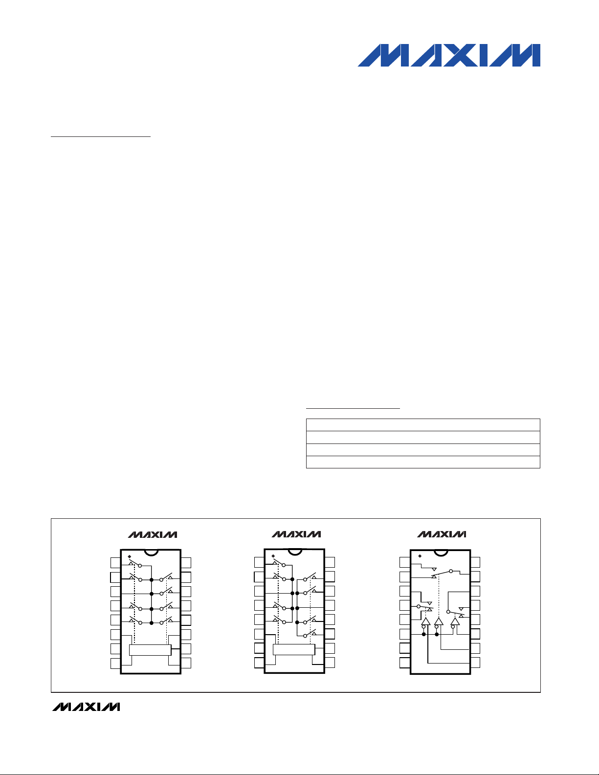
16
15
14
13
12
11
10
9
1
2
3
4
5
6
7
8
V+
NO2
NO1
NO0
NO3
ADDA
ADDB
ADDC
NO4
NO6
COM
NO7
NO5
INH
V-
GND
TOP VIEW
MAX4051
DIP/SO/QSOP
LOGIC
16
15
14
13
12
11
10
9
1
2
3
4
5
6
7
8
V+
COMB
COMC
NOC
NCC
ADDC
ADDB
ADDA
NOB
NCB
NOA
COMA
NCA
INH
V-
GND
MAX4053
DIP/SO/QSOP
16
15
14
13
12
11
10
9
1
2
3
4
5
6
7
8
V+
NO2A
NO1A
COMA
NO0A
NO3A
ADDA
ADDB
NO0B
NO2B
COMB
NO3B
NO1B
INH
V-
GND
MAX4052
DIP/SO/QSOP
LOGIC
___________________________________Pin Configurations/Functional Diagrams
19-0463; Rev 2; 10/05
PART
MAX4051ACPE
MAX4051ACSE
MAX4051ACEE 0°C to +70°C
0°C to +70°C
0°C to +70°C
TEMP RANGE PIN-PACKAGE
16 Plastic DIP
16 Narrow SO
16 QSOP
Ordering Information
Ordering Information continued at end of data sheet.
For pricing, delivery, and ordering information, please contact Maxim/Dallas Direct! at
1-888-629-4642, or visit Maxim’s website at www.maxim-ic.com.
MAX4051/A, MAX4052/A, MAX4053/A
Low-Voltage, CMOS Analog
Multiplexers/Switches
2 _______________________________________________________________________________________
ABSOLUTE MAXIMUM RATINGS
ELECTRICAL CHARACTERISTICS—Dual Supplies
(V+ = +4.5V to +5.5V, V- = -4.5V to -5.5V, TA= T
MIN
to T
MAX
, unless otherwise noted. Typical values are at TA= +25°C.)
Stresses beyond those listed under “Absolute Maximum Ratings” may cause permanent damage to the device. These are stress ratings only, and functional
operation of the device at these or any other conditions beyond those indicated in the operational sections of the specifications is not implied. Exposure to
absolute maximum rating conditions for extended periods may affect device reliability.
Voltages Referenced to GND
V+ ........................................................................-0.3V to +17V
V-..........................................................................+0.3V to -17V
V+ to V- ................................................................-0.3V to +17V
Voltage into Any Terminal (Note 1) ..........(V- - 2V) to (V+ + 2V)
or 30mA (whichever occurs first)
Continuous Current into Any Terminal..............................±30mA
Peak Current, NO or COM
(pulsed at 1ms, 10% duty cycle) .................................±100mA
Continuous Power Dissipation (T
A
= +70°C)
Plastic DIP (derate 10.53mW/°C above +70°C)............842mW
Narrow SO (derate 8.70mW/°C above +70°C)..............696mW
QSOP (derate 8.00mW/°C above +70°C) .....................640mW
CERDIP (derate 10.00mW/°C above +70°C) ................800mW
Operating Temperature Ranges
MAX405_C_ E/MAX405_AC_E .............................0°C to +70°C
MAX405_E_ E/MAX405_AE_E...........................-40°C to +85°C
MAX405_MJE/MAX405_AMJE ........................-55°C to +125°C
Storage Temperature Range .............................-65°C to +150°C
Lead Temperature (soldering, 10s) .................................+300°C
CONDITIONS
60 100
VV- V+V
COM
, V
NO
Analog Signal Range
Ω
125
R
ON
COM–NO On-Resistance
UNITS
MIN TYP MAX
(Note 2)
SYMBOL
TA= +25°C
C, E, M
V+ = 5V, V- = -5V, INO= 1mA,
V
COM
= ±3V
TA= +25°C 6
MAX4051A,
MAX4052A,
MAX4053A
V+ = 5V, V- = -5V,
INO= 1mA,
V
COM
= ±3V
TA= +25°C
Ω
12
∆R
ON
COM–NO On-Resistance
Match Between Channels
(Note 3)
MAX4051,
MAX4052,
MAX4053
V+ = 5.5V, V- = -5.5V,
VNO= 4.5V,
V
COM
= -4.5V
M
C, E -10 10
-100 100
MAX4051,
MAX4052,
MAX4053
TA= +25°C
V+ = 5V, V- = -5V,
INO= 1mA,
V
COM
= -3V, 0V, 3V
V+ = 5.5V, V- = -5.5V,
VNO= -4.5V,
V
COM
= 4.5V
M
nA
-100 100
I
NO(OFF)
NO Off-Leakage Current
(Note 5)
MAX4051A,
MAX4052A,
MAX4053A
C, E
TA= +25°C -0.1 0.002 0.1
-5 5
TA= +25°C
Ω
10
R
FLAT(ON)
COM–NO On-Resistance
Flatness (Note 4)
-1 0.002 1
MAX4051A,
MAX4052A,
MAX4053A
C, E, M
Note 1: Signals on any terminal exceeding V+ or V- are clamped by internal diodes. Limit forward-diode current to maximum
current rating.
C, E, M 12
C, E, M 18
C, E, M 15
PARAMETER
ANALOG SWITCH
MAX4051/A, MAX4052/A, MAX4053/A
Low-Voltage, CMOS Analog
Multiplexers/Switches
_______________________________________________________________________________________ 3
ELECTRICAL CHARACTERISTICS—Dual Supplies (continued)
(V+ = +4.5V to +5.5V, V- = -4.5V to -5.5V, TA= T
MIN
to T
MAX
, unless otherwise noted. Typical values are at TA= +25°C.)
TA= +25°C
M -100 100
MAX4051A
-1 0.002 1
C, E
C, E
TA= +25°C
CONDITIONS
-0.1 0.002 0.1
-2.5 2.5
M
C, E -10 10
-100 100
MAX4051
V+ = 5.5V, V- = -5.5V,
VNO= 4.5V,
V
COM
= -4.5V
M
C, E -5 5
-50 50
COM Off-Leakage
Current (Note 5)
MAX4052,
MAX4053
TA= +25°C
TA= +25°C -0.1 0.002 0.1
UNITS
MIN TYP MAX
(Note 2)
SYMBOLPARAMETER
M
-5 5
-100 100
MAX4052A,
MAX4053A
-1 0.002 1
TA= +25°C
M -100 100
MAX4051A
-1 0.002 1
C, E
C, E
TA= +25°C -0.1 0.002 0.1
-2.5 2.5
M
C, E -10 10
-100 100
MAX4051
V+ = 5.5V, V- = -5.5V,
VNO= -4.5V,
V
COM
= 4.5V
M
C, E
nA
-5 5
-50 50
I
COM(OFF)
MAX4052,
MAX4053
TA= +25°C
TA= +25°C -0.1 0.002 0.1
M
-5 5
-50 50
MAX4052A,
MAX4053A
-1 0.002 1
TA= +25°C
M -100 100
MAX4051A
-1 0.002 1
C, E
C, E
TA= +25°C -0.1 0.002 0.1
-2.5 2.5
M
C, E -10 10
-100 100
MAX4051
V+ = 5.5V, V- = -5.5V,
V
COM
= VNO= ±4.5V
M
C, E
nA
-5 5
-50 50
I
COM(ON)
COM On-Leakage
Current (Note 5)
MAX4052,
MAX4053
TA= +25°C
TA= +25°C -0.1 0.002 0.1
M
-5 5
-50 50
MAX4052A,
MAX4053A
-1 0.002 1
MAX4051/A, MAX4052/A, MAX4053/A
Low-Voltage, CMOS Analog
Multiplexers/Switches
4 _______________________________________________________________________________________
Note 2: The algebraic convention is used in this data sheet; the most negative value is shown in the minimum column.
Note 3: ∆R
ON
= R
ON(MAX)
- R
ON(MIN)
.
Note 4: Flatness is defined as the difference between the maximum and minimum value of on-resistance as measured over the
specified analog signal ranges; i.e., V
NO
= 3V to 0V and 0V to -3V.
Note 5: Leakage parameters are 100% tested at maximum-rated hot operating temperature, and guaranteed by correlation at
T
A
= +25°C.
Note 6: Guaranteed by design, not production tested.
C, E, M V2.4V
IH
ADD, INH Input Logic
Threshold High
TA= +25°C
TA= +25°C
CONDITIONS
ns
ns75 250t
TRANS
Transition Time Figure 2
210t
OPEN
Break-Before-Make Delay Figure 4
C, E, M
TA= +25°C
ns
50 175
225
t
ON
Turn-On Time (Note 6) Figure 3
TA= +25°C pF2C
NO(OFF)
NO Off-Capacitance VNO= GND, f = 1MHz, Figure 7
TA= +25°C
TA= +25°C
C, E, M V±2.7 ±8V+, V-Power-Supply Range
-1 0.1 1
TA= +25°C pF2C
COM(OFF)
COM Off-Capacitance
UNITS
MIN TYP MAX
(Note 2)
SYMBOLPARAMETER
V
COM
= GND, f = 1MHz, Figure 7
pC210QCharge Injection (Note 6)
CL= 1nF, RS= 0Ω, VNO= 0V,
Figure 5
C, E, M
µA
10
I+V+ Supply Current INH = ADD = 0V or V+
ELECTRICAL CHARACTERISTICS—Dual Supplies (continued)
(V+ = +4.5V to +5.5V, V- = -4.5V to -5.5V, TA= T
MIN
to T
MAX
, unless otherwise noted. Typical values are at TA= +25°C.)
C, E, M V0.8V
IL
ADD, INH Input Logic
Threshold Low
C, E, M µA-1 0.03 1IIH, I
IL
ADD, INH Input Current
Logic High or Low
V
ADD
, V
INH
= V+, 0V
C, E, M
TA= +25°C
ns
40 150
200
t
OFF
Turn-Off Time (Note 6) Figure 3
TA= +25°C pF8C
(ON)
Switch On-Capacitance
V
COM
= V
NO
= GND, f = 1MHz,
Figure 7
TA= +25°C dB<-90V
ISO
Off-Isolation
CL= 15pF, RL= 50Ω, f = 100kHz,
V
NO
= 1V
RMS
, Figure 6
TA= +25°C -1 0.1 1
C, E, M
µA
-10
I-V- Supply Current INH = ADD = 0V or V+
TA= +25°C dB<-90V
CT
Channel-to-Channel
Crosstalk
CL= 15pF, RL= 50Ω, f = 100kHz,
V
NO
= 1V
RMS
, Figure 6
DIGITAL I/O
SWITCH DYNAMIC CHARACTERISTICS
POWER SUPPLY
MAX4051/A, MAX4052/A, MAX4053/A
Low-Voltage, CMOS Analog
Multiplexers/Switches
_______________________________________________________________________________________ 5
ELECTRICAL CHARACTERISTICS—Single +5V Supply
(V+ = +4.5V to +5.5V, V- = 0V, TA= T
MIN
to T
MAX
, unless otherwise noted. Typical values are at TA= +25°C.)
C, E, M
TA= +25°C
Ω
125 225
Analog Signal Range
280
R
ON
COM–NO On-Resistance
V+ = 5V, INO= 1mA,
V
COM
= 3.5V
C, E, M
TA= +25°C
M
CONDITIONS
-100 100
V+ = 5.5V, VNO= 4.5V,
V
COM
= 0V
-1 0.002 1
C, E
TA= +25°C -1 0.002 1
-10 10
C, E
TA= +25°C -1 0.002 1
-10 10
V+ = 5.5V, VNO= 4.5V,
V
COM
= 0V
M
M
C, E -5 5
-50 50
V
MAX4052/A,
MAX4053/A
TA= +25°C
M -100 100
TA= +25°C
V+ = 5.5V, VNO= 0V,
V
COM
= 4.5V or 0V
M
nA
-50 50
I
COM(OFF)
COM Off-Leakage
Current (Note 5)
MAX4052/A,
MAX4053/A
-1 0.002 1
UNITS
MIN TYP MAX
(Note 2)
SYMBOLPARAMETER
MAX4051/A
-1 0.002 1
C, E
nA
V- V+V
COM
, V
NO
-10 10
-100 100
I
NO(OFF)
NO Off-Leakage Current
(Note 5)
V+ = 5.5V, VNO= 0V,
V
COM
= 4.5V
TA= +25°C
M -100 100
MAX4051/A
-1 0.002 1
C, E
TA= +25°C -1 0.002 1
-10 10
C, E -5 5
V+ = 5.5V,
V
COM
= VNO= 4.5V
C, E
TA= +25°C -1 0.002 1
-10 10
M
C, E -10 10
-100 100
MAX4051/A
M
nA
-100 100
I
COM(ON)
COM On-Leakage
Current (Note 5)
MAX4052/A,
MAX4053/A
C, E, M 0.8
C, E, M 2.4
V
V
V
IL
V
IH
ADD, INH Input Logic
Threshold Low
ADD, INH Input Logic
Threshold High
C, E, M -1 0.03 1V
ADD, VINH
= V+, 0V µAI
IH, IIL
ADD, INH Input Current
Logic High or Low
TA= +25°C -1 1
INH = ADD = 0V or V+ µAI+V+ Supply Current
C, E, M 10
ANALOG SWITCH
DIGITAL I/O
POWER SUPPLY
MAX4051/A, MAX4052/A, MAX4053/A
Low-Voltage, CMOS Analog
Multiplexers/Switches
6 _______________________________________________________________________________________
ELECTRICAL CHARACTERISTICS—Single +5V Supply (continued)
(V+ = +4.5V to +5.5V, V- = 0V, TA= T
MIN
to T
MAX
, unless otherwise noted. Typical values are at TA= +25°C.)
Note 2: The algebraic convention is used in this data sheet; the most negative value is shown in the minimum column.
Note 3: ∆R
ON
= R
ON(MAX)
- R
ON(MIN)
.
Note 4: Flatness is defined as the difference between the maximum and minimum value of on-resistance as measured over the
specified analog signal ranges; i.e., V
NO
= 3V to 0V and 0V to -3V.
Note 5: Leakage parameters are 100% tested at maximum-rated hot operating temperature, and guaranteed by correlation at
T
A
= +25°C.
Note 6: Guaranteed by design, not production tested.
TA= +25°C
C, E, M
CONDITIONS
ns30t
OPEN
Break-Before-Make Delay Figure 4
C, E, M
TA= +25°C
TA= +25°C
ns
ns
90 200
60 125
175
t
OFF
275
t
ON
Turn-On Time (Note 6) Figure 3
TA= +25°C dB<-90V
ISO
Off-Isolation
CL= 15pF, RL= 50Ω, f = 100kHz,
VNO= 1V
RMS
, Figure 6
TA= +25°C
Turn-Off Time (Note 6)
TA= +25°C dB<-90V
CT
Channel-to-Channel
Crosstalk
CL= 15pF, RL= 50Ω, f = 100kHz,
VNO= 1V
RMS
, Figure 6
Figure 3
UNITS
MIN TYP MAX
(Note 2)
SYMBOLPARAMETER
pC210QCharge Injection (Note 6)
CL= 1nF, RS= 0Ω, VNO= 0V,
Figure 5
DIGITAL I/OSWITCH DYNAMIC CHARACTERISTICS

MAX4051/A, MAX4052/A, MAX4053/A
Low-Voltage, CMOS Analog
Multiplexers/Switches
_______________________________________________________________________________________ 7
ELECTRICAL CHARACTERISTICS—Single +3V Supply
(V+ = +3.0V to +3.6V, V- = 0V, TA= T
MIN
to T
MAX
, unless otherwise noted. Typical values are at TA= +25°C.)
C, E, M
TA= +25°C
Ω
V+ = 3.6V,
V
COM
= VNO= 3V
250 525
Analog Signal Range
700
R
ON
COM–NO On-Resistance
INO= 1mA, V+ = 3V,
V
COM
= 1.5V
C, E, M
TA= +25°C
M
CONDITIONS
-100 100
V+ = 3.6V, VNO= 3V,
V
COM
= 0V
-1 0.002 1
C, E
TA= +25°C
C, E
-1 0.002 1
TA= +25°C
-10 10
-1 0.002 1
C, E
TA= +25°C -1 0.002 1
-10 10
V+ = 3.6V, VNO= 3V,
V
COM
= 0V
M
-10 10
M
C, E -5 5
-50 50
V
M
C, E -10 10
MAX4052/A,
MAX4053/A
TA= +25°C
M -100 100
TA= +25°C
V+ = 3.6V, VNO= 0V,
V
COM
= 3V
M
-100 100
nA
-50 50
I
COM(OFF)
COM Off-Leakage
Current (Note 5)
MAX4052/A,
MAX4053/A
-1 0.002 1
UNITS
MIN TYP MAX
(Note 2)
SYMBOLPARAMETER
MAX4051/A
-1 0.002 1
MAX4051/A
C, E
nA
M
nA
V- V+V
COM
, V
NO
-100 100
-10 10
I
COM(ON)
COM On-Leakage
Current (Note 5)
MAX4052/A,
MAX4053/A
-100 100
I
NO(OFF)
NO Off-Leakage Current
(Note 5)
V+ = 3.6V, VNO= 0V,
V
COM
= 3V
TA= +25°C
M -100 100
MAX4051/A
-1 0.002 1
C, E
TA= +25°C -1 0.002 1
-10 10
C, E -5 5
C, E, M 0.8
C, E, M 2.4
nA
V
IL
V
IH
ADD, INH Input Logic
Threshold Low
ADD, INH Input Logic
Threshold High
V
V
C, E, M -1 0.03 1I
IH, IIL
V
ADD, VINH
= V+, 0V
ADD, INH Input Current
Logic High or Low
µA
nA
TA= +25°C -1 1
I+ INH = ADD = 0V or V+V+ Supply Current µA
C, E, M 10
ANALOG SWITCH
DIGITAL I/O
POWER SUPPLY

MAX4051/A, MAX4052/A, MAX4053/A
Low-Voltage, CMOS Analog
Multiplexers/Switches
8 _______________________________________________________________________________________
ELECTRICAL CHARACTERISTICS—Single +3V Supply (continued)
(V+ = +3.0V to +3.6V, V- = 0V, TA= T
MIN
to T
MAX
, unless otherwise noted. Typical values are at TA= +25°C.)
TA= +25°C
C, E, M
CONDITIONS
ns90t
OPEN
Break-Before-Make Delay Figure 4
C, E, M
TA= +25°C
TA= +25°C
ns
ns
180 600
100 300
400
t
OFF
700
t
ON
Turn-On Time (Note 6) Figure 3
TA= +25°C dB<-90V
ISO
Off-Isolation
CL= 15pF, RL= 50Ω, f = 100kHz,
VNO= 1V
RMS
, Figure 6
TA= +25°C
Turn-Off Time (Note 6)
TA= +25°C dB<-90V
CT
Channel-to-Channel
Crosstalk
CL= 15pF, RL= 50Ω, f = 100kHz,
VNO= 1V
RMS
, Figure 6
Figure 3
UNITS
MIN TYP MAX
(Note 2)
SYMBOLPARAMETER
pC110QCharge Injection (Note 6)
CL= 1nF, RS= 0Ω, VNO= 0V,
Figure 5
Note 2: The algebraic convention is used in this data sheet; the most negative value is shown in the minimum column.
Note 3: ∆R
ON
= R
ON(MAX)
- R
ON(MIN)
.
Note 4: Flatness is defined as the difference between the maximum and minimum value of on-resistance as measured over the
specified analog signal ranges; i.e., V
NO
= 3V to 0V and 0V to -3V.
Note 5: Leakage parameters are 100% tested at maximum-rated hot operating temperature, and guaranteed by correlation at
T
A
= +25°C.
Note 6: Guaranteed by design, not production tested.
DIGITAL I/OSWITCH DYNAMIC CHARACTERISTICS

MAX4051/A, MAX4052/A, MAX4053/A
Low-Voltage, CMOS Analog
Multiplexers/Switches
_______________________________________________________________________________________ 9
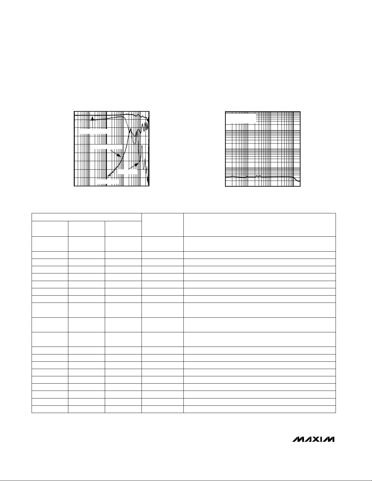
110
30
-5 -3 1
ON-RESISTANCE vs. V
COM
(DUAL SUPPLIES)
50
90
MAX4051/2/3-TOC1
V
COM
(V)
R
ON
(Ω)
-1 3
70
100
40
80
60
5-4 0-2 2 4
V± = ±5V
V± = ±3V
110
30
-5 -3 1
ON-RESISTANCE vs. V
COM
AND TEMPERATURE
(DUAL SUPPLIES)
50
90
MAX4051/2/3-TOC2
V
COM
(V)
R
ON
(Ω)
-1 3
70
100
40
80
60
5-4 0-2 2 4
V+ = 5V
V- = -5V
TA = +125°C
TA = +85°C
TA = +25°C
TA = -55°C
300
50
02
ON-RESISTANCE vs. V
COM
(SINGLE SUPPLY)
100
200
MAX4051/2/3-TOC3
V
COM
(V)
R
ON
(Ω)
4
150
250
275
225
75
175
125
153
V+ = 3V
V- = 0V
V+ = 5V
180
02
ON-RESISTANCE vs. V
COM
AND TEMPERATURE
(SINGLE SUPPLY)
100
MAX4051/2/3-TOC4
V
COM
(V)
R
ON
(Ω)
4
60
140
160
120
80
40
153
TA = +25°C
TA = -55°C
TA = +85°C
TA = +125°C
V+ = 5V
V- = 0V
-5 -3 1
CHARGE INJECTION vs. V
COM
-5
5
MAX4051/2/3-TOC7
V
COM
(V)
Qj (pC)
-1 3
0
5-4 0-2 2 4
V+ = 5V
V- = -5V
V+ = 5V
V- = 0V
0.1
OFF-LEAKAGE vs.
TEMPERATURE
1000
MAX4051/2/3-TOC5
TEMPERATURE (°C)
OFF-LEAKAGE (pA)
10
1
100
-50 12525-25 0 7550 100
V+ = 5.5V
V- = -5.5V
0.1
ON-LEAKAGE vs.
TEMPERATURE
1000
10,000
MAX4051/2/3-TOC6
TEMPERATURE (°C)
ON-LEAKAGE (pA)
10
1
100
-50 12525-25 0 7550 100
V+ = 5.5V
V- = -5.5V
0.1
SUPPLY CURRENT vs.
TEMPERATURE
10
MAX4051/2/3-TOC8
TEMPERATURE (°C)
I+, I- (nA)
1
-50 12525-25 0 7550 100
V+ = 5V
V- = -5V
V
EN
= VA = 0V, 5V
I+
I-
__________________________________________Typical Operating Characteristics
(V+ = +5V, V- = -5V, GND = 0V, TA= +25°C, unless otherwise noted.)
MAX4051/A, MAX4052/A, MAX4053/A
Low-Voltage, CMOS Analog
Multiplexers/Switches
10 ______________________________________________________________________________________
____________________________Typical Operating Characteristics (continued)
(V+ = +5V, V- = -5V, GND = 0V, TA= +25°C, unless otherwise noted.)
_____________________________________________________________Pin Descriptions
Digital Inhibit Input. Normally connect to GND. Can be driven
to logic high to set all switches off.
66
Negative Analog Supply Voltage Input. Connect to GND for
single-supply operation.
77
Ground. Connect to digital ground. (Analog signals have no
ground reference; they are limited to V+ and V-.)
88
Digital Address “C” Input—9
Digital Address “B” Input910
Analog Switch “B” Normally Open Input——
Analog Switch “B” Normally Closed Input——
Analog Switch “A” Normally Open Input——
Analog Switch “A” Normally Closed Input——
Analog Switch “B” Common3—
Analog Switch “B” Inputs 0–31, 2, 4, 5—
Analog Switch Common—3
Analog Switch Inputs 0–7—
1, 2, 4, 5, 12,
13, 14, 15
FUNCTION
Analog Switch “C” Normally Closed Input——
Analog Switch “C” Normally Open Input——
Analog Switch “C” Common——
Digital Address “A” Input1011
Analog Switch “A” Inputs 0–311, 12, 14, 15—
Analog Switch “A” Common13—
Note: NO, NC, and COM pins are identical and interchangeable. Any may be considered an input or output; signals pass equally
well in both directions.
INH
6
V-7
GND8
ADDC11
ADDB10
NOB1
NCB2
NOA3
NCA5
COMB15
NO0B–NO3B—
COM—
NO0–NO7—
NAME
NCC12
NOC13
COMC14
ADDA9
NO0A–NO3A—
COMA4
MAX4051/
MAX4051A
MAX4052/
MAX4052A
MAX4053/
MAX4053A
Positive Analog and Digital Supply Voltage Input1616 V+16
PIN
0
-10
-20
-30
-40
-50
LOSS (dB)
-60
-70
-80
-90
FREQUENCY RESPONSE
INSERTION LOSS
OFF-ISOLATION
ON PHASE
50Ω IN/OUT
0.01 0.1 1 10 100 300
FREQUENCY (MHz)
5
0
MAX4051/2/3-09
-5
-10
-15
-20
-25
-30
-35
-40
THD (%)
PHASE (DEGREES)
TOTAL HARMONIC DISTORTION
vs. FREQUENCY
100
V± = ±5V
600Ω IN AND OUT
10
1
0.1
0.01
10 100 1k 10k
FREQUENCY (Hz)
MAX4051/2/3-10

__________Applications Information
Power-Supply Considerations
Overview
The MAX4051/MAX4052/MAX4053 and MAX4051A/
MAX4052A/MAX4053A construction is typical of most
CMOS analog switches. They have three supply pins:
V+, V-, and GND. V+ and V- are used to drive the internal CMOS switches and set the limits of the analog voltage on any switch. Reverse ESD-protection diodes are
internally connected between each analog signal pin
and both V+ and V-. If any analog signal exceeds V+ or
V-, one of these diodes will conduct. During normal
operation, these (and other) reverse-biased ESD diodes
leak, forming the only current drawn from V+ or V-.
Virtually all the analog leakage current comes from the
ESD diodes. Although the ESD diodes on a given signal
pin are identical, and therefore fairly well balanced,
they are reverse biased differently. Each is biased by
either V+ or V- and the analog signal. This means their
leakages will vary as the signal varies. The difference in
the two diode leakages to the V+ and V- pins constitutes the analog signal path leakage current. All analog
leakage current flows between each pin and one of the
supply terminals, not to the other switch terminal. This is
why both sides of a given switch can show leakage currents of either the same or opposite polarity.
There is no connection between the analog signal
paths and GND.
MAX4051/A, MAX4052/A, MAX4053/A
Low-Voltage, CMOS Analog
Multiplexers/Switches
______________________________________________________________________________________ 11
X1
Table 1. Truth Table/Switch Programming
X X All switches open All switches open All switches open
0 0 COM–NO0
COMB–NO0B,
COMA–NO0A
COMA–NCA,
COMB–NCB,
COMC–NCC
00
0 1 COM–NO1
COMB–NO1B,
COMA–NO1A
COMA–NOA,
COMB–NCB,
COMC–NCC
00
1 1 COM–NO3
COMB–NO3B,
COMA–NO3A
COMA–NOA,
COMB–NOB,
COMC–NCC
1 0 COM–NO2
COMB–NO2B,
COMA–NO2A
COMA–NCA,
COMB–NOB,
COMC–NCC
00
00
0 1 COM–NO5
COMB–NO1B,
COMA–NO1A
COMA–NOA,
COMB–NCB,
COMC–NOC
0 0 COM–NO4
COMB–NO0B,
COMA–NO0A
COMA–NCA,
COMB–NCB,
COMC–NOC
10
10
1 1 COM–NO7
COMB–NO3B,
COMA–NO3A
COMA–NOA,
COMB–NOB,
COMC–NOC
1 0 COM–NO6
COMB–NO2B,
COMA–NO2A
COMA–NCA,
COMB–NOB,
COMC–NOC
10
10
X = Don’t care * ADDC not present on MAX4052.
Note: NO and COM pins are identical and interchangeable. Either may be considered an input or output; signals pass equally well
in either direction.
ON SWITCHESADDRESS BITS
ADDB ADDA
MAX4051/
MAX4051A
MAX4052/
MAX4052A
MAX4053/
MAX4053A
ADDC*
INH

MAX4051/A, MAX4052/A, MAX4053/A
V+ and GND power the internal logic and logic-level
translators, and set both the input and output logic limits. The logic-level translators convert the logic levels
into switched V+ and V- signals to drive the gates of
the analog signals. This drive signal is the only connection between the logic supplies (and signals) and the
analog supplies. V+ and V- have ESD-protection
diodes to GND.
The logic-level thresholds are TTL/CMOS compatible
when V+ is +5V. As V+ rises, the threshold increases
slightly, so when V+ reaches +12V, the threshold is
about 3.1V; above the TTL-guaranteed high-level minimum of 2.8V, but still compatible with CMOS outputs.
Bipolar Supplies
These devices operate with bipolar supplies between
±3.0V and ±8V. The V+ and V- supplies need not be
symmetrical, but their sum cannot exceed the absolute
maximum rating of +17V.
Single Supply
These devices operate from a single supply between
+3V and +16V when V- is connected to GND. All of the
bipolar precautions must be observed. At room temperature, they actually “work” with a single supply at near
or below +1.7V, although as supply voltage decreases,
switch on-resistance and switching times become very
high.
Overvoltage Protection
Proper power-supply sequencing is recommended for
all CMOS devices. Do not exceed the absolute maximum ratings, because stresses beyond the listed ratings can cause permanent damage to the devices.
Always sequence V+ on first, then V-, followed by the
logic inputs (NO) and by COM. If power-supply
sequencing is not possible, add two small signal diodes
(D1, D2) in series with the supply pins for overvoltage
protection (Figure 1).
Adding diodes reduces the analog signal range to one
diode drop below V+ and one diode drop above V-, but
does not affect the devices’ low switch resistance and
low leakage characteristics. Device operation is
unchanged, and the difference between V+ and Vshould not exceed 17V. These protection diodes are
not recommended when using a single supply if signal
levels must extend to ground.
High-Frequency Performance
In 50Ω systems, signal response is reasonably flat up
to 50MHz (see Typical Operating Characteristics).
Above 20MHz, the on response has several minor
peaks which are highly layout dependent. The problem
is not turning the switch on, but turning it off. The offstate switch acts like a capacitor, and passes higher
frequencies with less attenuation. At 10MHz, off isolation is about -45dB in 50Ω systems, becoming worse
(approximately 20dB per decade) as frequency
increases. Higher circuit impedances also make off isolation worse. Adjacent channel attenuation is about 3dB
above that of a bare IC socket, and is entirely due to
capacitive coupling.
Low-Voltage, CMOS Analog
Multiplexers/Switches
12 ______________________________________________________________________________________
COM NO
V-
V+
* INTERNAL PROTECTION DIODES
D2
D1EXTERNAL BLOCKING DIODE
EXTERNAL BLOCKING DIODE
V-
V+
MAX4051/A
MAX4052/A
MAX4053/A
*
*
*
*
Figure 1. Overvoltage Protection Using External Blocking
Diodes

MAX4051/A, MAX4052/A, MAX4053/A
Low-Voltage, CMOS Analog
Multiplexers/Switches
______________________________________________________________________________________ 13
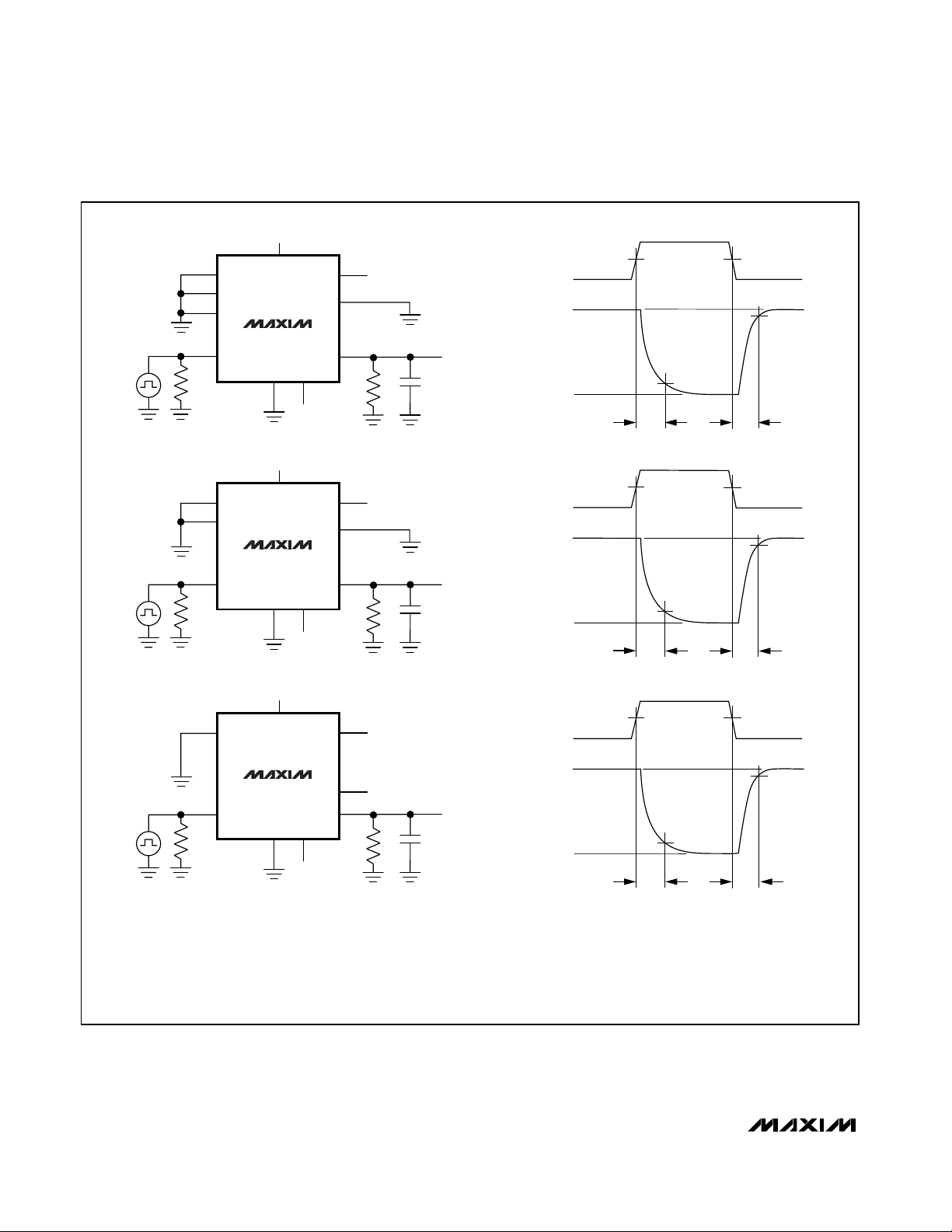
50%
t
TRANS
V+
0V
V
NO0
V
OUT
V
ADD
0V
V
NO7
90%
90%
t
TRANS
50%
t
TRANS
V+
0V
V
NO0
V
OUT
V
ADD
0V
V
NO3
90%
90%
t
TRANS
50%
t
TRANS
V+
0V
V
NC
V
OUT
V
ADD
0V
V
NO
90%
90%
t
TRANS
V+
V
OUT
V
ADD
V
ADD
V-
GND
V+
ADDB
V-
ADDC
ADDA
INH
NO0
NO1–NO6
NO7
COM
V+
V-
MAX4051/A
300Ω
50Ω
35pF
V+
V
OUT
V-
GND
V+
ADDB
V-
ADDA
INH
NO0
NO1–NO2
NO3
COM
V+
V-
MAX4052/A
300Ω
50Ω
35pF
V+
V
OUT
V-
GND
V+
V-
ADD
V
ADD
INH
NO
NC
COM
V-
V+
MAX4053/A
300Ω
50Ω
35pF
V- = 0V FOR SINGLE-SUPPLY OPERATION.
REPEAT TEST FOR EACH SECTION.
Figure 2. Address Transition Time
______________________________________________Test Circuits/Timing Diagrams
50%
t
OFF
V+
0V
V
NO0
V
OUT
V
INH
0V
90%
90%
t
ON
50%
t
OFF
V+
0V
V
NO0
V
OUT
V
INH
0V
90%
90%
t
ON
50%
t
OFF
V+
0V
V
NO_
V
OUT
V
INH
0V
90%
90%
t
ON
V+
V
OUT
V
INH
V
INH
V
INH
V-
GND
V+
ADDB
V-
ADDC
ADDA
INH
NO0
NO1–NO7
COM
V+
MAX4051/A
300Ω
50Ω
35pF
V+
V
OUT
V-
GND
V+
ADDB
V-
ADDA
INH
NO0
NO1–NO3
COM
V+
MAX4052/A
300Ω
50Ω
35pF
V+
V
OUT
V-
GND
V+
V-
ADD
INH
NO
NC
COM
V+
V-
MAX4053/A
300Ω
35pF
50Ω
V- = 0V FOR SINGLE-SUPPLY OPERATION.
REPEAT TEST FOR EACH SECTION.
Figure 3. Enable Switching Time
MAX4051/A, MAX4052/A, MAX4053/A
Low-Voltage, CMOS Analog
Multiplexers/Switches
14 ______________________________________________________________________________________

MAX4051/A, MAX4052/A, MAX4053/A
Low-Voltage, CMOS Analog
Multiplexers/Switches
______________________________________________________________________________________ 15
50%
V+
0V
V
NO_
V
OUT
V
ADD
0V
80%
t
OPEN
V+
V
OUT
V
ADD
V
ADD
V
ADD
V-
GND
V+
ADDB
V-
ADDC
ADDA
INH
NO0–N07
COM
V+
MAX4051/A
300Ω
50Ω
35pF
V+
V
OUT
V-
GND
V+
ADDB
V-
ADDA
INH
NO0–NO3
COM
V+
MAX4052/A
300Ω
35pF
V+
V
OUT
V-
GND
V+
V-
ADD
INH
NO, NC
COM
V+
MAX4053/A
300Ω
35pF
50Ω
50Ω
V- = 0V FOR SINGLE-SUPPLY OPERATION.
REPEAT TEST FOR EACH SECTION.
t
R
< 20ns
t
F
< 20ns
Figure 4. Break-Before-Make Interval
0V
V+
V
INH
∆ V
OUT
IS THE MEASURED VOLTAGE DUE TO CHARGE
TRANSFER ERROR Q WHEN THE CHANNEL TURNS OFF.
∆ V
OUT
V- = 0V FOR SINGLE-SUPPLY OPERATION.
REPEAT TEST FOR EACH SECTION.
Q = ∆ V
OUT
X C
L
V
OUT
V+
V
OUT
VNO = 0V
V
INH
V-
GND
V+
ADDB
V-
ADDC
CHANNEL
SELECT
ADDA
INH
NO
COM
MAX4051/A
MAX4052/A
MAX4053/A
50Ω
CL = 1000pF
Figure 5. Charge Injection

MAX4051/A, MAX4052/A, MAX4053/A
Low-Voltage, CMOS Analog
Multiplexers/Switches
16 ______________________________________________________________________________________
MEASUREMENTS ARE STANDARDIZED AGAINST SHORT AT SOCKET TERMINALS.
OFF-ISOLATION IS MEASURED BETWEEN COM AND "OFF" NO TERMINAL ON EACH SWITCH.
ON-LOSS IS MEASURED BETWEEN COM AND "ON" NO TERMINAL ON EACH SWITCH.
CROSSTALK (MAX4052 AND MAX4053) IS MEASURED FROM ONE CHANNEL (A, B, C) TO ALL OTHER CHANNELS.
SIGNAL DIRECTION THROUGH SWITCH IS REVERSED; WORST VALUES ARE RECORDED.
V+
V
OUT
V
IN
V-
GND
V+
V
IN
V
OUT
MEAS.
NETWORK
ANALYZER
50Ω 50Ω
50Ω
OFF-ISOLATION = 20log
ON-LOSS = 20log
CROSSTALK = 20log
50Ω
REF.
ADDB
V-
V
OUT
V
IN
V
OUT
V
IN
ADDC
CHANNEL
SELECT
ADDA
INH
NO
COM
10nF
10nF
MAX4051/A
MAX4052/A
MAX4053/A
Figure 6. Off-Isolation, On-Loss, and Crosstalk
V+
V-
GND
V+
ADDB
V-
ADDC
CHANNEL
SELECT
1MHz
CAPACITANCE
ANALYZER
ADDA
INH
NO
NO
COM
MAX4051/A
MAX4052/A
MAX4053/A
Figure 7. NO/COM Capacitance

MAX4051/A, MAX4052/A, MAX4053/A
Low-Voltage, CMOS Analog
Multiplexers/Switches
______________________________________________________________________________________ 17
16 CERDIP**-55°C to +125°CMAX4052MJE
16 QSOP
16 Narrow SO-40°C to +85°C
-40°C to +85°CMAX4052EEE
MAX4052ESE
Dice*
16 QSOP0°C to +70°C
0°C to +70°CMAX4052C/D
MAX4052CEE
16 Narrow SO
16 Plastic DIP0°C to +70°C
0°C to +70°CMAX4052CSE
MAX4052CPE
16 Plastic DIP-40°C to +85°CMAX4052EPE
16 CERDIP**
16 QSOP-40°C to +85°C
-55°C to +125°CMAX4052AMJE
MAX4052AEEE
16 Plastic DIP
16 QSOP0°C to +70°C
-40°C to +85°CMAX4052AEPE
MAX4052ACEE
16 Narrow SO
16 Plastic DIP0°C to +70°C
0°C to +70°CMAX4052ACSE
MAX4052ACPE
16 Narrow SO-40°C to +85°CMAX4052AESE
16 CERDIP**
16 QSOP-40°C to +85°C
-55°C to +125°CMAX4051MJE
MAX4051EEE
16 Narrow SO-40°C to +85°CMAX4051ESE
16 Plastic DIP
Dice*0°C to +70°C
-40°C to +85°CMAX4051EPE
MAX4051C/D
16 QSOP
16 Narrow SO
16 Plastic DIP0°C to +70°C
0°C to +70°C
0°C to +70°CMAX4051CEE
MAX4051CSE
MAX4051CPE
16 CERDIP**
16 QSOP-40°C to +85°C
-55°C to +125°CMAX4051AMJE
MAX4051AEEE
16 Narrow SO
16 Plastic DIP
PIN-PACKAGETEMP RANGE
-40°C to +85°C
-40°C to +85°CMAX4051AESE
MAX4051AEPE
PART
16 CERDIP**-55°C to +125°CMAX4053MJE
16 QSOP
16 Narrow SO-40°C to +85°C
-40°C to +85°CMAX4053EEE
MAX4053ESE
Dice*
16 QSOP0°C to +70°C
0°C to +70°CMAX4053C/D
MAX4053CEE
16 Narrow SO
16 Plastic DIP0°C to +70°C
0°C to +70°CMAX4053CSE
MAX4053CPE
16 Plastic DIP-40°C to +85°CMAX4053EPE
16 CERDIP**
16 QSOP-40°C to +85°C
-55°C to +125°CMAX4053AMJE
MAX4053AEEE
16 Plastic DIP
16 QSOP0°C to +70°C
-40°C to +85°CMAX4053AEPE
MAX4053ACEE
16 Narrow SO
16 Plastic DIP0°C to +70°C
0°C to +70°CMAX4053ACSE
MAX4053ACPE
16 Narrow SO-40°C to +85°CMAX4053AESE
PIN-PACKAGETEMP RANGEPART
* Contact factory for dice specifications.
** Contact factory for availability.
Chip Information
TRANSISTOR COUNT: 161
SUBSTRATE CONNECTED TO V+.
___________________________________________Ordering Information (continued)

MAX4051/A, MAX4052/A, MAX4053/A
Low-Voltage, CMOS Analog
Multiplexers/Switches
18 ______________________________________________________________________________________
Package Information
(The package drawing(s) in this data sheet may not reflect the most current specifications. For the latest package outline information,
go to www.maxim-ic.com/packages
.)
PDIPN.EPS

Maxim cannot assume responsibility for use of any circuitry other than circuitry entirely embodied in a Maxim product. No circuit patent licenses are
implied. Maxim reserves the right to change the circuitry and specifications without notice at any time.
Maxim Integrated Products, 120 San Gabriel Drive, Sunnyvale, CA 94086 (408) 737-7600___________________ 19
© 2005 Maxim Integrated Products Printed USA is a registered trademark of Maxim Integrated Products.
QSOP.EPS
E
1
1
21-0055
PACKAGE OUTLINE, QSOP .150", .025" LEAD PITCH
SOICN .EPS
PACKAGE OUTLINE, .150" SOIC
1
1
21-0041
B
REV.DOCUMENT CONTROL NO.APPROVAL
PROPRIETARY INFORMATION
TITLE:
TOP VIEW
FRONT VIEW
MAX
0.010
0.069
0.019
0.157
0.010
INCHES
0.150
0.007
E
C
DIM
0.014
0.004
B
A1
MIN
0.053A
0.19
3.80 4.00
0.25
MILLIMETERS
0.10
0.35
1.35
MIN
0.49
0.25
MAX
1.75
0.050
0.016L
0.40 1.27
0.3940.386D
D
MINDIM
D
INCHES
MAX
9.80 10.00
MILLIMETERS
MIN
MAX
16
AC
0.337 0.344 AB8.758.55 14
0.189 0.197 AA5.004.80 8
N MS012
N
SIDE VIEW
H 0.2440.228 5.80 6.20
e 0.050 BSC 1.27 BSC
C
HE
e
B
A1
A
D
0∞-8∞
L
1
VARIATIONS:
Package Information (continued)
(The package drawing(s) in this data sheet may not reflect the most current specifications. For the latest package outline information,
go to www.maxim-ic.com/packages
.)
MAX4051/A, MAX4052/A, MAX4053/A
Low-Voltage, CMOS Analog
Multiplexers/Switches
 Loading...