

General Description
The MAX4028/MAX4029 are 5V, triple/quad, 2:1 voltagefeedback multiplexer-amplifiers with input clamps and a
fixed gain of +2V/V (6dB). Channel 1 (IN1A and IN1B)
inputs are clamped to the video sync tip of the input signal, while the remaining inputs can be clamped to either
the video sync tip or the video sync of channel 1 (IN1_).
The latter is referred to as a key clamp and is pin selectable. Selectable clamp/key-clamp inputs and fixed-gain
video output buffers make the MAX4028/MAX4029 ideal
for video-source switching applications such as automotive entertainment systems, video projectors, and displays/TVs. Both devices have 20ns channel switching
times and low ±10mV
P-P
switching transients, making
them ideal for high-speed video switching applications
such as on-screen display (OSD) insertion.
The MAX4028/MAX4029 have a -3dB large-signal (2V
P-P
)
bandwidth of 130MHz, a -3dB small-signal bandwidth of
210MHz, and a 300V/µs slew rate. Low differential gain
and phase errors of 0.2% and 0.4°, respectively, make
these devices ideal for broadcast video applications.
The MAX4028/MAX4029 are specified over the -40°C to
+85°C extended temperature range and are offered in
16-pin and 20-pin TSSOP/SO packages.
Applications
In-Car Navigation/Entertainment
Blade Servers
Security Systems
Video Projectors
Displays and Digital Televisions
Broadcast and Graphics Video
Set-Top Boxes
Notebook Computers
Video Crosspoint Switching
Features
♦ Single +5V Operation
♦ Independently Selectable Sync-Tip or
Key-Clamp Inputs
♦ Adjustable Key-Clamp Voltage
♦ 130MHz Large-Signal -3dB Bandwidth
♦ 210MHz Small-Signal -3dB Bandwidth
♦ 300V/µs Slew Rate
♦ 20ns Switching Time
♦ Ultra-Low ±10mV
P-P
Switching Transient
♦ 0.2% Differential Gain/0.4° Phase Error
♦ Low-Power, High-Impedance Disable Mode
MAX4028/MAX4029
Triple/Quad, 2:1 Video
Multiplexer-Amplifiers with Input Clamps
________________________________________________________________ Maxim Integrated Products 1
Ordering Information
MAX4028
MAX4029
75Ω
75Ω
IN1A
V
CC
OUT1
CLAMP
A/B
+5V
C
IN
0.1µF
0.01µF
0.1µF
1kΩ
1kΩ
C
IN
0.1µF
IN1B
CLAMP
75Ω
75Ω
IN2A
OUT2
DISABLE
CLAMP/KEY_2
CLAMP
C
IN
0.1µF
R
KEYREF
6kΩ
1kΩ
1kΩ
C
IN
0.1µF
IN2B
KEYREF
CLAMP
KEY/CLAMP
CONTROL
75Ω CABLE
75Ω CABLE
75Ω CABLE
75Ω CABLE
75Ω
75Ω CABLE
75Ω
75Ω CABLE
Typical Operating Circuit
19-3240; Rev 0; 3/04
For pricing, delivery, and ordering information, please contact Maxim/Dallas Direct! at
1-888-629-4642, or visit Maxim’s website at www.maxim-ic.com.
EVALUATION KIT
AVAILABLE
Pin Configurations appear at end of data sheet.
PART TEMP RANGE PIN-PACKAGE
MAX4028EUE
-40°C to +85°C 16 TSSOP
MAX4028EWE
-40°C to +85°C 16 Wide SO
MAX4029EUP
-40°C to +85°C 20 TSSOP
MAX4029EWP
-40°C to +85°C 20 Wide SO
Selector Guide
PART
NO. OF 2:1
MUX-AMPS
GAIN
MAX4028 3 2V/V
MAX4029 4 2V/V
MAX4028/MAX4029
Triple/Quad, 2:1 Video
Multiplexer-Amplifiers with Input Clamps
2 _______________________________________________________________________________________
ABSOLUTE MAXIMUM RATINGS
DC ELECTRICAL CHARACTERISTICS
(VCC= +5V, GND = 0V, RL= 150Ω to GND, V
DISABLE
= +5V, R
KEYREF
= 6kΩ, CIN= 0.1µF to GND, TA= T
MIN
to T
MAX
, unless otherwise
noted. Typical values are at T
A
= +25°C.) (Note 2)
Stresses beyond those listed under “Absolute Maximum Ratings” may cause permanent damage to the device. These are stress ratings only, and functional
operation of the device at these or any other conditions beyond those indicated in the operational sections of the specifications is not implied. Exposure to
absolute maximum rating conditions for extended periods may affect device reliability.
Supply Voltage (VCCto GND) ..................................-0.3V to +6V
IN_A, IN_B, OUT_.......................................-0.3V to (V
CC
+ 0.3V)
DISABLE, A/B, KEYREF, CLAMP/KEY_......-0.3V to (V
CC
+ 0.3V)
Current Into IN_A, IN_B ...................................................±0.5mA
Short-Circuit Duration (V
OUT
to GND)........................Continuous
Short-Circuit Duration (V
OUT
to VCC) .............................(Note 1)
Continuous Power Dissipation (T
A
= +70°C)
16-Pin TSSOP (derate 9.4mW/°C above +70°C) .........755mW
16-Pin Wide SO (derate 9.5mW/°C above +70°C) ......762mW
20-Pin TSSOP (derate 11mW/°C above +70°C) ..........879mW
20-Pin Wide SO (derate 10mW/°C above +70°C) .......800mW
Operating Temperature Range ...........................-40°C to +85°C
Junction Temperature......................................................+150°C
Storage Temperature Range .............................-65°C to +150°C
Lead Temperature (soldering, 10s) .................................+300°C
PARAMETER
CONDITIONS MIN TYP MAX
UNITS
Operating Supply Voltage Range V
CC
Guaranteed by PSRR 4.5 5.5 V
MAX4028, RL = ∞ 29 40
Quiescent Supply Current I
CC
MAX4029, RL = ∞ 38 55
mA
MAX4028 9 15
Disable Supply Current V
DISABLE
= 0V
MAX4029 11 20
mA
Clamp (Note 3) 0.32 0.4 0.48
Output Clamp Voltage V
CLAMP
Key clamp (Note 4) 1.1
V
Input Clamping Current I
IN
Input voltage = input clamp + 0.5V 5 18 µA
Clamp Voltage Matching
Measured at output 10 mV
Clamp Voltage Drift
Measured at output 80
µV/°C
Input Resistance R
IN
7
MΩ
Output Resistance R
OUT
0.7 Ω
Disable Output Resistance R
OUT
V
DISABLE
= 0V 2 kΩ
Power-Supply Rejection Ratio PSRR 4.5V < VCC < 5.5V (Note 5) 48 58 dB
Voltage Gain A
VCL
1.9 2.0 2.1 V/V
Channel-to-Channel Gain Matching
∆A
VCL
±1 ±2 %
Output-Voltage High V
OH
V
CLAMP
+ 2.4
V
Output-Voltage Low V
OL
V
Output Current I
OUT
30 mA
LOGIC INPUT CHARACTERISTICS (DISABLE , A/B, CLAMP/KEY_)
Logic-Low Threshold V
IL
0.8 V
Logic-High Threshold V
IH
2.0 V
Logic-Low Input Current I
IL
VIL = 0V 6.6 25 µA
Logic-High Input Current I
IH
VIH = V
CC
1.2 25 µA
Note 1: Do not short V
OUT
to VCC.
SYMBOL
∆V
TC
CLAMP
VCLAMP
V
CLAMP
MAX4028/MAX4029
Triple/Quad, 2:1 Video
Multiplexer-Amplifiers with Input Clamps
_______________________________________________________________________________________ 3
AC ELECTRICAL CHARACTERISTICS
(VCC= +5V, GND = 0V, RL= 150Ω to GND, V
DISABLE
= +5V, R
KEYREF
= 6kΩ, CIN= 0.1µF, TA= T
MIN
to T
MAX
, unless otherwise noted.
Typical values are at T
A
= +25°C.)
Note 2: All devices are 100% production tested at T
A
= +25°C. Specifications over temperature are guaranteed by design.
Note 3: The clamp voltage at the input is V
CLAMP
(measured at the output) divided by gain + VBE.
Note 4: The key-clamp voltage is above the sync-tip clamp voltage by approximately 0.7V, and is adjusted by varying R
KEYREF
.
Note 5: Measured at f = 100Hz at thermal equilibrium.
PARAMETER
SYMBOL
CONDITIONS MIN TYP MAX
UNITS
Small-Signal -3dB Bandwidth BW
SS
V
OUT
= 100mV
P-P
210
MHz
Large-Signal -3dB Bandwidth BW
LS
V
OUT
= 2V
P-P
130
MHz
Small-Signal 0.1dB Gain Flatness
Bandwidth
V
OUT
= 100mV
P-P
30
MHz
Large-Signal 0.1dB Gain Flatness
Bandwidth
V
OUT
= 2V
P-P
30
MHz
Slew Rate SR V
OUT
= 2V
P-P
300 V/µs
Settling Time to 0.1% t
S
V
OUT
= 2V step 20 ns
Power-Supply Rejection Ratio PSRR f = 100kHz 55 dB
Output Impedance Z
O
f = 100kHz 0.7 Ω
Differential Gain Error DG 5-step modulated staircase 0.2 %
Differential Phase Error DP 5-step modulated staircase 0.4
degrees
Group Delay D/dT f = 3.58MHz or 4.43MHz 1.0 ns
Peak Signal to RMS Noise SNR 100kHz to 30MHz 70 dB
Channel-to-Channel Crosstalk X
TALK
f = 100kHz 73 dB
A/B Crosstalk
f = 100kHz 91 dB
Off-Isolation A
ISO
V
OUT_
= 2V
P-P
, f = 100kHz 108 dB
Droop D
R
Guaranteed by input clamp current 2 %
SWITCHING CHARACTERISTICS
Channel Switching Time t
SW
20 ns
Enable Time t
ON
0.1 µs
Disable Time t
OFF
0.1 µs
Switching Transient ±10
mV
P-P
BW
BW
X
0.1dBSS
0.1dBLS
TALKAB
MAX4028/MAX4029
Triple/Quad, 2:1 Video
Multiplexer-Amplifiers with Input Clamps
4 _______________________________________________________________________________________
Typical Operating Characteristics
(VCC= +5V, GND = 0V, V
DISABLE
= +5V, RL= 150Ω to GND, CIN= 0.1µF, R
KEYREF
= 6.04kΩ ±1%, TA= +25°C, unless otherwise
noted.)
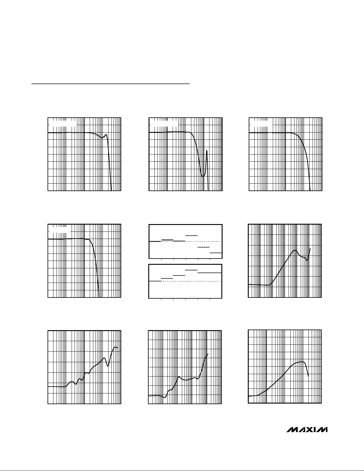
SMALL-SIGNAL BANDWIDTH
vs. FREQUENCY
MAX4028 toc01
FREQUENCY (Hz)
SMALL-SIGNAL BANDWIDTH (dB)
100M10M1M
-1
0
1
2
3
4
5
6
7
8
-2
100k 1G
V
OUT
= 100mV
P-P
SMALL-SIGNAL GAIN FLATNESS
vs. FREQUENCY
MAX4028 toc02
FREQUENCY (Hz)
GAIN FLATNESS (dB)
100M10M1M
5.3
5.4
5.5
5.6
5.7
5.8
5.9
6.0
6.1
6.2
5.2
100k 1G
V
OUT
= 100mV
P-P
LARGE-SIGNAL BANDWIDTH
vs. FREQUENCY
MAX4028 toc03
FREQUENCY (Hz)
LARGE-SIGNAL BANDWIDTH (dB)
100M10M1M
-1
0
1
2
3
4
5
6
7
8
-2
100k 1G
V
OUT
= 2V
P-P
LARGE-SIGNAL GAIN FLATNESS
vs. FREQUENCY
MAX4028 toc04
FREQUENCY (Hz)
LARGE-SIGNAL GAIN FLATNESS (dB)
100M10M1M
5.3
5.4
5.5
5.6
5.7
5.8
5.9
6.0
6.1
6.2
5.2
100k 1G
V
OUT
= 2V
P-P
DIFFERENTIAL GAIN AND PHASE
MAX4028 toc05
DIFFERENTIAL GAIN (%)
6th
5th4th3rd2nd
-0.1
-0.2
-0.3
0
0.1
0.2
0.3
1st
DIFFERENTIAL PHASE (deg)
6th
5th4th3rd2nd
-0.02
-0.04
-0.06
0
0.02
0.04
0.06
1st
POWER-SUPPLY REJECTION RATIO
vs. FREQUENCY
MAX4028 toc06
FREQUENCY (Hz)
PSRR (dB)
100M10M1M100k10k
-60
-50
-40
-30
-20
-10
0
-70
1k 1G
OFF-ISOLATION
vs. FREQUENCY
MAX4028 toc07
FREQUENCY (Hz)
OFF-ISOLATION (dB)
100M10M1M
-120
-100
-80
-60
-40
-20
0
-140
100k 1G
ALL-HOSTILE CROSSTALK (CHANNEL TO
CHANNEL) vs. FREQUENCY
MAX4028 toc08
FREQUENCY (Hz)
CROSSTALK (dB)
100M10M100k 1M
-70
-60
-50
-40
-30
-20
-10
0
-80
10k 1G
ALL-HOSTILE CROSSTALK (A TO B ON ANY
CHANNEL) vs. FREQUENCY
MAX4028 toc09
FREQUENCY (Hz)
CROSSTALK (dB)
100M10M1M
-90
-80
-70
-60
-50
-40
-30
-20
-10
0
-100
100k 1G

MAX4028/MAX4029
Triple/Quad, 2:1 Video
Multiplexer-Amplifiers with Input Clamps
_______________________________________________________________________________________ 5
OUTPUT IMPEDANCE
vs. FREQUENCY
MAX4028 toc10
FREQUENCY (Hz)
OUTPUT IMPEDANCE (Ω)
100M10M1M100k
1
10
100
0.1
10k 1G
INPUT-VOLTAGE NOISE DENSITY
vs. FREQUENCY
MAX4028 toc11
FREQUENCY (Hz)
INPUT-VOLTAGE NOISE DENSITY (nV/√Hz)
100k10k1k10010
10
100
1000
1
11M
LARGE-SIGNAL TRANSIENT RESPONSE
MAX4028 toc12
10ns/div
1.6VDC
V
IN
500mV/div
V
OUT
1V/div
SMALL-SIGNAL TRANSIENT RESPONSE
MAX4028 toc13
10ns/div
1.6VDC
V
IN
25mV/div
SIGNAL 2
50mV/div
CHANNEL-SWITCHING TRANSIENT
MAX4028 toc14
20ns/div
5VDC
0VDC
A/B
2.5V/div
V
OUT
20mV/div
CHANNEL-SWITCHING TIME
(CHA = 1.5VDC, CHB = 1VDC)
MAX4028 toc15
20ns/div
5VDC
0VDC
A/B
2.5V/div
V
OUT
500mV/div
ENABLE RESPONSE TIME
(V
OUT
= 0.5V)
MAX4028 toc16
50ns/div
5VDC
0VDC
0.5VDC
0VDC
ENABLE
2.5V/div
V
OUT
250mV/div
SMALL-SIGNAL BANDWIDTH
vs. FREQUENCY
MAX4028 toc17
FREQUENCY (Hz)
SMALL-SIGNAL BANDWIDTH (dB)
100M10M1M
2
3
4
5
6
7
8
9
10
11
1
100k 1G
C
LOAD
= 15pF
C
LOAD
= 10pF
C
LOAD
= 5pF
OPTIMAL ISOLATION RESISTANCE
vs. CAPACITIVE LOAD
MAX4028 toc18
C
LOAD
(pF)
OPTIMAL ISOLATION RESISTANCE (Ω)
20015010050
5
10
15
20
25
30
0
0250
Typical Operating Characteristics (continued)
(VCC= +5V, GND = 0V, V
DISABLE
= +5V, RL= 150Ω to GND, CIN= 0.1µF, R
KEYREF
= 6.04kΩ ±1%, TA= +25°C, unless otherwise
noted.)

MAX4028/MAX4029
Triple/Quad, 2:1 Video
Multiplexer-Amplifiers with Input Clamps
6 _______________________________________________________________________________________
Pin Description
PIN
MAX4028
NAME FUNCTION
—1IN4A Amplifier Input 4A
12IN3A Amplifier Input 3A
23IN2A Amplifier Input 2A
34IN1A Amplifier Input 1A
45 A/B
Channel-Select Input. Drive A/B high or leave floating to select channel A.
Drive A/B low to select channel B.
56KEYREF
Key-Clamp Reference Output. Connect an external resistor from KEYREF to GND to
generate the key-clamp voltage.
67IN1B Amplifier Input 1B
78IN2B Amplifier Input 2B
89IN3B Amplifier Input 3B
—10IN4B Amplifier Input 4B
—11OUT4 Amplifier Output 4
912
Output 3 Clamp or Key-Clamp Input. Drive CLAMP/KEY_3 high to clamp OUT3.
Drive CLAMP/KEY_3 low to key clamp OUT3.
10 13 GND Ground
11 14 OUT3 Amplifier Output 3
12 15
Output 2 Clamp or Key-Clamp Input. Drive CLAMP/KEY_2 high to clamp OUT2.
Drive CLAMP/KEY_2 low to key clamp OUT2.
13 16 OUT2 Amplifier Output 2
14 17 V
CC
Power-Supply Voltage. Bypass VCC to GND with 0.1µF and 0.01µF capacitors as
close to the pin as possible.
Typical Operating Characteristics (continued)
(VCC= +5V, GND = 0V, V
DISABLE
= +5V, RL= 150Ω to GND, CIN= 0.1µF, R
KEYREF
= 6.04kΩ ±1%, TA= +25°C, unless otherwise
noted.)
KEY-CLAMP REFERENCE VOLTAGE
vs. R
KEYREF
MAX4028 toc20
R
KEYREF
(kΩ)
KEY-CLAMP REFERENCE VOLTAGE (V)
119753
0.2
0.4
0.6
0.8
1.0
1.2
1.4
1.6
1.8
0
113
0.43
CLAMP VOLTAGE
vs. TEMPERATURE
0.42
0.41
0.40
0.39
CLAMP VOLTAGE (V)
0.38
0.37
-50 100
TEMPERATURE (°C)
7550250-25
MAX4029
CLAMP/KEY_3
CLAMP/KEY_2
MAX4028 toc19

Detailed Description
The MAX4028/MAX4029 are 5V, triple/quad, 2:1 voltagefeedback multiplexer-amplifiers with input clamps and a
fixed gain of +2V/V (6dB). Channel 1 (IN1A and IN1B)
inputs are clamped to the video sync tip of the input
IN1_ channel, while the remaining inputs can be
clamped to either the video sync tip of the respective
input channel (IN_A and IN_B) or the video sync of
channel 1 (IN1_). The latter is referred to as a key
clamp and is pin selectable. Selectable clamp/keyclamp inputs and fixed-gain video output buffers make
the MAX4028/MAX4029 ideal for video-source switching
applications such as automotive entertainment systems,
video projectors, and displays/TVs. Both devices have
20ns channel switching times and low ±10mV
P-P
switching transients, making them ideal for both high-speed
video switching applications such as OSD insertion.
The MAX4028/MAX4029 have a -3dB large-signal (2V
P-P
)
bandwidth of 130MHz, a -3dB small-signal bandwidth of
210MHz, and a 300V/µs slew rate. Low differential gain
and phase errors of 0.2% and 0.4°, respectively, make
these devices ideal for broadcast video applications.
Sync Tip and Key Clamps
The MAX4028/MAX4029 have AC-coupled inputs, with
either a sync tip or key clamp to provide bias for the
video signal. Channel 1 of the MAX4028/MAX4029
always has a sync tip clamp at the input, while the
remaining channels are selectable as either sync tip or
key clamps to accommodate the various video waveforms (see the Clamp/Key-Clamp Settings for Video
Formats section). The value of the sync-tip clamp voltage
is set internally for the lowest value, consistent with linear
operation, and cannot be adjusted. The key-clamp voltage is adjustable, to compensate for variations in the
voltage between component video inputs such as Linear
RGB, YPbPr, and Y-C, by varying R
KEYREF
. The key-
clamp voltage can be computed from:
V
Key-Clamp
= 0.40 + 2000/[(5000 x R
KEYREF
) /
(5000 + R
KEYREF
)]
MAX4028/MAX4029
Triple/Quad, 2:1 Video
Multiplexer-Amplifiers with Input Clamps
_______________________________________________________________________________________ 7
Pin Description (continued)
PIN
NAME FUNCTION
15 18 OUT1 Amplifier Output 1
16 19 DISABLE
Disable Input. Pull DISABLE high for normal operation. Drive DISABLE low to disable
all outputs.
—20
Output 4 Clamp or Key-Clamp Input. Drive CLAMP/KEY_4 high to clamp OUT4.
Drive CLAMP/KEY_4 low to key clamp OUT4.
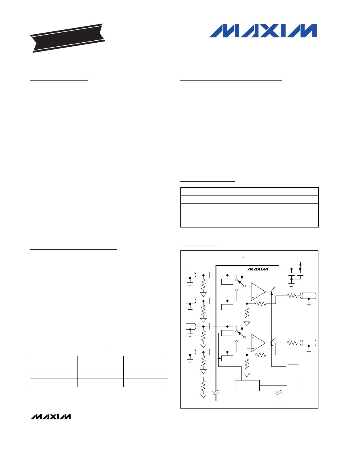
Figure 1. MAX4029 Functional Diagram
MAX4028 MAX4029
CLAMP/KEY_4
IN1A
CLAMP
IN1B
CLAMP
1kΩ
IN2A
CLAMP/
KEY
CLAMP
IN2B
CLAMP/
KEY
CLAMP/KEY_2
IN3A
IN3B
CLAMP/KEY_3
A/B
IN4A
IN4B
CLAMP/KEY_4
KEYREF
CLAMP
CLAMP/
KEY
CLAMP
CLAMP/
KEY
CLAMP
CLAMP/
KEY
CLAMP
CLAMP/
KEY
CLAMP
CLAMP
VOLTAGE
1kΩ
1kΩ
1kΩ
GND
V
CC
1kΩ
1kΩ
1kΩ
1kΩ
MAX4029
OUT1
OUT2
OUT3
OUT4
DISABLE

MAX4028/MAX4029
Therefore, a 6kΩ resistor will produce a 1.13V keyclamp voltage as shown in Figure 2. The clamp voltage
(V
CLAMP
) is measured at the output; the voltage at the
input is V
CLAMP
(sync tip or key clamp) divided by the
gain (+2V/V) + VBE.
In order for these clamps (sync tip or key) to work properly, the input must be coupled with a 0.1µF capacitor (typ)
with low leakage (<1µA to 2µA, max). Without proper coupling, the clamp voltage will change during the horizontal
line time causing the “black level” to vary, changing the
image brightness from left to right on the display. In addi-
tion to the capacitor, a low resistance (≤75Ω) is required
on the source side to return the capacitor to ground. The
clamps used here are active devices with the coupling
capacitor serving two functions; first, as a charge reservoir to maintain the clamp voltage, and second, as the
compensation capacitor for the clamp itself. If an input is
not used, it must be terminated to avoid causing oscillations that could couple with another input.
In general, a sync-tip clamp is used for composite video
(Cvbs), gamma-corrected primaries (R’G’B’), and the
luma signal (Y) in S-video. A key clamp is preferred for
component color difference signals (Pb and Pr), linear
primaries (RGB in PCs), and chroma (C) in S-video. The
rule is to sync tip clamp a signal if sync is present and
key clamp all others. Several examples are given in the
Clamp/Key-Clamp Settings for Video Formats section.
Clamp/Key-Clamp Settings for Video Formats
Tables 1 and 2 provide the clamp settings on the
MAX4028/MAX4029 to interface with various video formats.
Low-Power, High-Impedance Disable Mode
All parts feature a low-power, high-impedance disable
mode that is activated by driving the DISABLE input
low. Placing the amplifier in disable mode reduces the
quiescent supply current and places the output impedance at 2kΩ typically. Multiple devices can be paralleled to construct larger switch matrices by connecting
the outputs of several devices together and disabling
all but one of the paralleled amplifiers’ outputs.
Triple/Quad, 2:1 Video
Multiplexer-Amplifiers with Input Clamps
8 _______________________________________________________________________________________
KEY-CLAMP REFERENCE VOLTAGE
vs. R
KEYREF
MAX4028 fig02
R
KEYREF
(kΩ)
KEY-CLAMP REFERENCE VOLTAGE (V)
119753
0.2
0.4
0.6
0.8
1.0
1.2
1.4
1.6
1.8
0
113
Figure 2. Key-Clamp Reference Voltage vs. R
KEYREF
Table 1. MAX4028 Clamp Settings for Video Formats
INPUT FORMAT CLAMP/KEY
1 Cvbs1 Clamp
2 Cvbs2 Clamp
3 Cvbs3 Clamp
R, G, B have sync on all.
INPUT FORMAT CLAMP/KEY
1GsClamp
2BKey
3RKey
Gs, B, R have sync only on Green.
INPUT FORMAT CLAMP/KEY
1YClamp
2CKey
3 Cvbs Clamp
INPUT FORMAT CLAMP/KEY
1G’Clamp
2B’Clamp
3R’Clamp
INPUT FORMAT CLAMP/KEY
1YClamp
2PbKey
3PrKey

The MAX4028/MAX4029 have a fixed gain of +2V/V that
is internally set with two 1kΩ thin-film resistors. The
impedance of the internal feedback resistors must be
taken into account when operating multiple MAX4028/
MAX4029s in large multiplexer applications.
Applications Information
Video Line Driver
The MAX4028/MAX4029 are well suited to drive coaxial
transmission lines when the cable is terminated at both
ends, as shown in Figure 3, where the fixed gain of
+2V/V compensates for the loss in the resistors, RT.
Driving Capacitive Loads
A correctly terminated transmission line is purely resistive and presents no capacitive load to the amplifier.
Reactive loads decrease phase margin and may produce excessive ringing and oscillation.
Another concern when driving capacitive loads is the
amplifier’s output impedance, which appears inductive
at high frequencies. This inductance forms an L-C reso-
nant circuit with the capacitive load, which causes
peaking in the frequency response and degrades the
amplifier’s phase margin.
MAX4028/MAX4029
Triple/Quad, 2:1 Video
Multiplexer-Amplifiers with Input Clamps
_______________________________________________________________________________________ 9
Table 2. MAX4029 Clamp Settings for Video Formats
INPUT FORMAT CLAMP/KEY
1 Cvbs1 Clamp
2 Cvbs2 Clamp
3 Cvbs3 Clamp
4 Cvbs4 Clamp
Gs, B, R have sync only on Green.
INPUT FORMAT CLAMP/KEY
1H-Sync Clamp
2GKey
3BKey
4RKey
R, G, B have sync on none.
INPUT FORMAT CLAMP/KEY
1YClamp
2CKey
3 Cvbs Clamp
4 Cvbs Clamp
R, G, B have sync on all.
R
T
75Ω
R
T
75Ω
R
T
75Ω
OUT_
IN_A
IN_B
A/B DISABLE
0.1µF
75Ω CABLE
75Ω CABLE
R
T
75Ω
0.1µF
75Ω CABLE
R
KEYREF
MAX4028
MAX4029
CLAMP
Figure 3. Video Line Driver
INPUT FORMAT CLAMP/KEY
1GsClamp
2RKey
3BKey
4 Cvbs Clamp
INPUT FORMAT CLAMP/KEY
1YClamp
2PrKey
3PbKey
4 Cvbs Clamp
INPUT FORMAT CLAMP/KEY
1 Cvbs Clamp
2G’Clamp
3B’Clamp
4R’Clamp

MAX4028/MAX4029
Although the MAX4028/MAX4029 are optimized for AC
performance and are not designed to drive highly
capacitive loads, they are capable of driving up to
15pF without oscillations. However, some peaking may
occur in the frequency domain (Figure 4). To drive larger capacitive loads or to reduce ringing, add an isolation resistor between the amplifier’s output and the load
(Figure 5). The value of R
ISO
depends on the circuit’s
gain (+2V/V) and the capacitive load (Figure 6). Also
note that the isolation resistor forms a divider that
decreases the voltage delivered to the load.
Layout and Power-Supply Bypassing
The MAX4028/MAX4029 have high bandwidths and
consequently require careful board layout, including
the possible use of constant-impedance microstrip or
stripline techniques.
To realize the full AC performance of these high-speed
amplifiers, pay careful attention to power-supply
bypassing and board layout. The PC board should
have at least two layers: a signal and power layer on
one side, and a large, low-impedance ground plane on
the other side. The ground plane should be as free of
voids as possible. Whether or not a constant-impedance board is used, it is best to observe the following
guidelines when designing the board:
1) Do not use wire-wrapped boards or breadboards.
2) Do not use IC sockets; they increase parasitic
capacitance and inductance.
3) Keep signal lines as short and straight as possible.
Do not make 90° turns; round all corners.
4) Observe high-frequency bypassing techniques to
maintain the amplifier’s accuracy and stability.
5) Use surface-mount components. They generally
have shorter bodies and lower parasitic reactance,
yielding better high-frequency performance than
through-hole components.
Triple/Quad, 2:1 Video
Multiplexer-Amplifiers with Input Clamps
10 ______________________________________________________________________________________
SMALL-SIGNAL BANDWIDTH
vs. FREQUENCY
MAX4028 fig04
FREQUENCY (Hz)
SMALL-SIGNAL BANDWIDTH (dB)
100M10M1M
2
3
4
5
6
7
8
9
10
11
1
100k 1G
C
LOAD
= 15pF
C
LOAD
= 10pF
C
LOAD
= 5pF
Figure 4. Small-Signal Gain vs. Frequency with Capacitive
Load and No Isolation Resistor
R
ISO
R
L
C
L
R
T
75Ω
OUT_
IN_A
IN_B
A/B DISABLE
0.1µF
75Ω CABLE
R
T
75Ω
0.1µF
75Ω CABLE
R
KEYREF
MAX4028
MAX4029
CLAMP
Figure 5. Using an Isolation Resistor (R
ISO
) for a High-
Capacitive Load
OPTIMAL ISOLATION RESISTANCE
vs. CAPACITIVE LOAD
MAX4028 fig06
C
LOAD
(pF)
OPTIMAL ISOLATION RESISTANCE (Ω)
20015010050
5
10
15
20
25
30
0
0 250
Figure 6. Optimal Isolation Resistance vs. Capacitive Load

The bypass capacitors should include a 0.1µF, ceramic
surface-mount capacitor between VCCand the ground
plane, located as close to the package as possible.
Optionally, place a 10µF capacitor at the power supply’s
point-of-entry to the PC board to ensure the integrity of
incoming supplies. The power-supply traces should lead
directly from the capacitor to the VCCpin. To minimize
parasitic inductance, keep PC traces short and use surface-mount components.
If input termination resistors and output back-termination
resistors are used, they should be surface-mount types,
and should be placed as close to the IC pins as possible.
MAX4028/MAX4029
Triple/Quad, 2:1 Video
Multiplexer-Amplifiers with Input Clamps
______________________________________________________________________________________ 11
16
15
14
13
12
11
10
9
1
2
3
4
5
6
7
8
IN3A
DISABLE
OUT1
V
CC
OUT2
CLAMP/KEY_2
OUT3
GND
CLAMP/KEY_3
TOP VIEW
MAX4028
TSSOP/SO
IN2A
IN1A
IN1B
A/B
KEYREF
IN2B
IN3B
20
19
18
17
16
15
14
13
1
2
3
4
5
6
7
8
CLAMP/KEY_4
DISABLE
OUT1
V
CC
IN1A
IN2A
IN3A
IN4A
OUT2
CLAMP/KEY_2
OUT3
GNDIN2B
IN1B
KEYREF
A/B
12
11
9
10
CLAMP/KEY_3
OUT4IN4B
IN3B
MAX4029
TSSOP/SO
Pin Configurations
Chip Information
TRANSISTOR COUNT: 1032
PROCESS: Bipolar

MAX4028/MAX4029
Triple/Quad, 2:1 Video
Multiplexer-Amplifiers with Input Clamps
12 ______________________________________________________________________________________
Package Information
(The package drawing(s) in this data sheet may not reflect the most current specifications. For the latest package outline information,
go to www.maxim-ic.com/packages
.)
TSSOP4.40mm.EPS
PACKAGE OUTLINE, TSSOP 4.40mm BODY
21-0066
1
1
I

MAX4028/MAX4029
Triple/Quad, 2:1 Video
Multiplexer-Amplifiers with Input Clamps
Maxim cannot assume responsibility for use of any circuitry other than circuitry entirely embodied in a Maxim product. No circuit patent licenses are
implied. Maxim reserves the right to change the circuitry and specifications without notice at any time.
Maxim Integrated Products, 120 San Gabriel Drive, Sunnyvale, CA 94086 408-737-7600 ____________________ 13
© 2004 Maxim Integrated Products Printed USA is a registered trademark of Maxim Integrated Products.
Package Information (continued)
(The package drawing(s) in this data sheet may not reflect the most current specifications. For the latest package outline information,
go to www.maxim-ic.com/packages
.)
SOICW.EPS
PACKAGE OUTLINE, .300" SOIC
1
1
21-0042
B
REV.DOCUMENT CONTROL NO.APPROVAL
PROPRIETARY INFORMATION
TITLE:
TOP VIEW
FRONT VIEW
MAX
0.012
0.104
0.019
0.299
0.013
INCHES
0.291
0.009
E
C
DIM
0.014
0.004
B
A1
MIN
0.093A
0.23
7.40 7.60
0.32
MILLIMETERS
0.10
0.35
2.35
MIN
0.49
0.30
MAX
2.65
0.050
0.016L
0.40 1.27
0.5120.496D
D
MINDIM
D
INCHES
MAX
12.60 13.00
MILLIMETERS
MIN
MAX
20
AC
0.447 0.463 AB11.7511.35 18
0.398 0.413 AA10.5010.10 16
N MS013
SIDE VIEW
H 0.4190.394 10.00 10.65
e 0.050 1.27
D 0.6140.598 15.20 2415.60 AD
D 0.7130.697 17.70 2818.10 AE
H
E
N
D
A1
B
e
A
0∞-8∞
C
L
1
VARIATIONS:
 Loading...