

Page 1
General Description
The MAX4027 is a triple, wideband, 2-channel, noninverting gain-of-two video amplifier with input multiplexing, capable of driving up to two back-terminated video
loads. The MAX4027 features current-mode feedback
amplifiers configured for a gain of two (+6dB) with a
-3dB large-signal bandwidth of 200MHz. The device
has low (0.012%/0.014°) differential gain and phase
errors, and operates from ±5V supplies.
The MAX4027 is ideal for use in broadcast and graphics video systems because of the low 2pF input capacitance, channel-to-channel switching time of only 15ns,
and wide 62MHz, large-signal 0.1dB bandwidth. Highimpedance output disabling allows the MAX4027 to be
incorporated into large switching arrays with minimal
interaction with the source. Specified over the -40°C to
+85°C extended temperature range, the MAX4027 is
available in 14-pin SO and TSSOP packages.
Applications
Video Source Selection (Multiplexing)
Picture in Picture (PIP) Insertion
Crosspoint Expansion
Coaxial Cable Drivers
Supports VGA to UXGA (1600 x 1200) Resolution
Enterprise Class (Blade) Servers
Keyboard-Video-Mouse (KVM)
Features
♦ Excellent Video Specifications:
75MHz Small-Signal 0.1dB Gain Flatness
62MHz Large-Signal 0.1dB Gain Flatness
0.012%/0.014° Differential Gain/Phase Error
♦ VGA to UXGA Resolution
♦ High Speed:
200MHz 2V
P-P
-3dB Bandwidth
1100V/µs Slew Rate
15ns Settling Time to 0.1%
♦ Internal Gain of 2V/V Compensates for Output
Back Termination
♦ Fast Switching:
15ns Channel-Switching Time
260mV
P-P
Switching Transient
♦ Drives Two Back-Terminated Video Loads
♦ High-Impedance Output Disable
MAX4027
225MHz, Triple, 2-Channel Video
Multiplexer-Amplifier
________________________________________________________________ Maxim Integrated Products 1
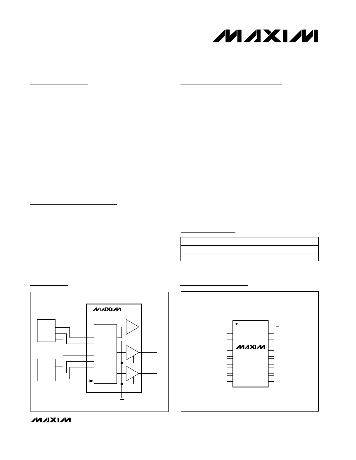
Pin Configuration
Ordering Information
VIDEO
SOURCE
1
R
IN1A
IN2A
IN3A
IN1B
IN2B
IN3B
G
B
R
G
B
TRIPLE
2:1
MUX
A/B EN
OUT1
OUT2
OUT3
R
G
B
VIDEO
SOURCE
2
MAX4027
x 2
x 2
x 2
14
13
12
11
10
9
8
1
2
3
4
5
6
7
A/B
OUT1
V
CC
OUT2GND
IN3A
IN2A
IN1A
TOP VIEW
MAX4027
V
EE
OUT3
ENIN3B
IN2B
IN1B
SO/TSSOP
Typical Operating Circuit
19-2987; Rev 0; 9/03
For pricing, delivery, and ordering information, please contact Maxim/Dallas Direct! at
1-888-629-4642, or visit Maxim’s website at www.maxim-ic.com.
PART TEMP RANGE PIN-PACKAGE
MAX4027ESD -40°C to +85°C 14 SO
MAX4027EUD -40°C to +85°C 14 TSSOP
Page 2
MAX4027
225MHz, Triple, 2-Channel Video
Multiplexer-Amplifier
2 _______________________________________________________________________________________
ABSOLUTE MAXIMUM RATINGS
DC ELECTRICAL CHARACTERISTICS
(VCC= 5V, VEE= -5V, V
IN_ _
= 0V, RL= 150Ω to GND, TA= -40°C to +85°C. Typical values are at TA= +25°C.) (Note 2)
Stresses beyond those listed under “Absolute Maximum Ratings” may cause permanent damage to the device. These are stress ratings only, and functional
operation of the device at these or any other conditions beyond those indicated in the operational sections of the specifications is not implied. Exposure to
absolute maximum rating conditions for extended periods may affect device reliability.
Note 1: Continuous power-dissipation rating must also be observed.
Positive Supply Voltage (V
CC
to GND) ..................................+6V
Negative Supply Voltage (V
EE
to GND) ..................................-6V
Amplifier Input Voltage (IN_ _) .........(V
EE
- 0.3V) to (VCC+ 0.3V)
Digital Input Voltage (EN, A/B)...................-0.3V to (V
CC
+ 0.3V)
Output Short Circuit to GND (Note 1).........................Continuous
Output Short Circuit to V
CC
or VEE...........................................5s
Continuous Power Dissipation (T
A
= +70°C)
14-Pin TSSOP (derate 9.1mW/°C above +70°C) .........727mW
14-Pin SO (derate 8.3mW/°C above +70°C)................667mW
Operating Temperature Range ...........................-40°C to +85°C
Storage Temperature Range .............................-65°C to +150°C
Junction Temperature .....................................................+150°C
Lead Temperature (soldering, 10s) .................................+300°C
)
Operating Supply Voltage Range
Positive Supply Current I
Negative Supply Current I
Input Voltage Range V
Input Offset Voltage V
Input Offset-Voltage Matching ∆V
Voltage Gain A
Input Offset-Voltage Temperature
Coefficient
Input Bias Current I
Input Resistance R
DC Output Resistance R
Disabled Output Resistance R
DC Power-Supply Rejection Ratio PSRR VCC = +4.5V to +5.5V, VEE = -4.5V to -5.5V 60 86 dB
Output Voltage Swing V
Output Short-Circuit Current I
LOGIC CHARACTERISTICS (EN, A/B)
Logic-Low Threshold V
Logic-High Threshold V
Logic-Low Input Current I
Logic-High Input Current I
PARAMETER SYMBOL CONDITIONS MIN TYP MAX UNITS
V
CC
V
CC
IN_ _
TCV
OUT
OUT(d
OUT_
Inferred from the PSRR test
EE
EN = GND 31 39
EN = 5V 17 24
EN = GND 28 36
EE
EN = 5V 15 21
Inferred from voltage gain ±1.25 ±1.75 V
TA = +25°C±1±6
OS
TA = -40°C to +85°C ±11
Channel to channel ±1 ±12 mV
OS
V
V
OS
B
IN
SC
IL
IH
IL
IH
= ±2.5V 1.9 2.0 2.1 V/V
OUT_
TA = +25°C ±2 ±10
TA = -40°C to +85°C ±18
V
= -1.25V to
IN_ _
+1.25V
EN = 5V, V
VIL = 0V -4 -20 µA
VIH = +5.5V, VCC = +5.5V 350 600 µA
OUT_
+4.5 +5.0 +5.5
-4.5 -5.0 -5.5
1 µV/°C
Channel on 100 400 kΩ
Channel off 1 20 MΩ
10 mΩ
= -2.5V to +2.5V (Note 3) 1.6 kΩ
±2.5 ±3.5 V
±143 mA
0.8 V
2.0 V
V
mA
mA
mV
µA
Page 3
MAX4027
225MHz, Triple, 2-Channel Video
Multiplexer-Amplifier
_______________________________________________________________________________________ 3
AC ELECTRICAL CHARACTERISTICS
(VCC= 5V, VEE= -5V, V
IN_ _
= 0V, RIN= 75Ω to GND, RL= 150Ω to GND, TA= +25°C, unless otherwise noted.)
Note 2: Limits are 100% production tested at T
A
= +25°C. Limits over the operating temperature range are guaranteed by design.
Note 3: Disabled output resistance includes the internal feedback network.
Note 4: Input test signal is NTSC composite with 5-step staircase, of 40 IRE per step, modulated with 3.58MHz color subcarrier.
Note 5: See the Timing Diagram (Figure 2).
Note 6: Channel-switching time specified for switching between input channels; does not include signal rise/fall times for switching
between channels with different input voltages.
Note 7: Output enable/disable delay times do not include amplifier output slewing times.
Note 8: Switching transient measured while switching between two grounded channels.
)
)
PARAMETER SYMBOL CONDITIONS MIN TYP MAX UNITS
AMPLIFIER CHARACTERISTICS
Small-Signal -3dB Bandwidth BW
Small-Signal Bandwidth for
±0.1dB Gain Flatness
Large-Signal -3dB Bandwidth BW
Large-Signal Bandwidth for
±0.1dB Gain Flatness
Slew Rate SR V
Settling Time to 0.1% t
Differential Gain Error DG 5-step modulated staircase (Note 4) 0.012 %
Differential Phase Error DP 5-step modulated staircase (Note 4) 0.014 degrees
Delay Between Channels t
Channel-to-Channel Crosstalk X
A/B Crosstalk V
Output Impedance Z
Total Harmonic Distortion THD V
Off-Isolation A
Output Capacitance C
Input Capacitance C
Input-Voltage Noise Density e
Input-Current Noise Density i
SWITCHING CHARACTERISTICS
Channel-Switching Time t
Enable Delay Time t
Disable Delay Time t
Switching Transient V
SSVIN_ _
BW
LS(0.1
LSVIN_ _
BW
LS(0.1
S
D
TALKVIN_ _
OUT
ISO
OUT
IN
n
n
SW
PDE
PDD
TRAN
= 20mV
P-P
V
= 20mV
IN_ _
V
IN_ _
IN_ _
V
IN_ _
V
IN_ _
IN_ _
P-P
= 1V
P-P
= 1V
P-P
= 1V
P-P
= 1V
P-P
= 1V
, tR = 100ps 0.1 ns
P-P
= ±1V
= ±1V
, f = 10MHz -61 dB
P-P
, f = 10MHz -80 dB
P-P
f = 10MHz 1 Ω
= 2V
OUT_
V
OUT_
, f = 10MHz 64 dBc
P-P
= 2V
, f = 10MHz, RS = 75Ω -83 dB
P-P
Channel on or off 3 pF
Channel on or off 2 pF
f = 100kHz 6.5 nV/√Hz
f = 100kHz 6.5 pA/√Hz
(Notes 5, 6) 15 ns
(Notes 5, 7) 20 ns
(Notes 5, 7) 25 ns
(Note 8) 260 mV
225 MHz
75 MHz
200 MHz
62 MHz
1100 V/µs
15 ns
P-P
Page 4
MAX4027
225MHz, Triple, 2-Channel Video
Multiplexer-Amplifier
4 _______________________________________________________________________________________
Typical Operating Characteristics
(VCC= +5V, VEE= -5V, RL= 150Ω to GND, TA= +25°C, unless otherwise noted.)
SMALL-SIGNAL FREQUENCY RESPONSE
MAX4027 toc01
FREQUENCY (Hz)
GAIN (dB)
100M10M
-6
-5
-4
-3
-2
-1
0
1
2
3
-7
1M 1G
V
IN_ _
= 20mV
P-P
AV = +2V/V
SMALL-SIGNAL GAIN FLATNESS
vs. FREQUENCY
MAX4027 toc02
FREQUENCY (Hz)
GAIN (dB)
100M10M
-0.6
-0.5
-0.4
-0.3
-0.2
-0.1
0
0.1
0.2
0.3
-0.7
1M 1G
V
IN_ _
= 20mV
P-P
AV = +2V/V
LARGE-SIGNAL FREQUENCY RESPONSE
MAX4027 toc03
FREQUENCY (Hz)
GAIN (dB)
100M10M
-6
-5
-4
-3
-2
-1
0
1
2
3
-7
1M 1G
AV = +2V/V
V
OUT_
= 4V
P-P
V
OUT_
= 2V
P-P
LARGE-SIGNAL GAIN FLATNESS
vs. FREQUENCY
MAX4027 toc04
FREQUENCY (Hz)
GAIN (dB)
100M10M
-0.6
-0.5
-0.4
-0.3
-0.2
-0.1
0
0.1
0.2
0.3
-0.7
1M 1G
AV = +2V/V
V
OUT_
= 4V
P-P
V
OUT_
= 2V
P-P
CHANNEL-TO-CHANNEL GAIN MATCHING
vs. FREQUENCY
MAX4027 toc05
FREQUENCY (Hz)
CHANNEL-TO-CHANNEL GAIN MATCHING (dB)
10M
-0.4
-0.3
-0.2
-0.1
0
0.1
0.2
0.3
0.4
0.5
-0.5
1M 100M
V
OUT_
= 2V
P-P
DIFFERENTIAL GAIN AND PHASE
MAX4027 toc06
DIFFERENTIAL PHASE (DEG)
5th3rd
-0.010
0
0.010
0.020
-0.020
-0.010
0
0.010
0.020
-0.020
1st 2nd 4th 6th
5th3rd1st 2nd 4th 6th
DIFFERENTIAL GAIN (%)
POWER-SUPPLY REJECTION RATIO
vs. FREQUENCY
MAX4027 toc07
FREQUENCY (Hz)
PSRR (dB)
10M1M
-60
-55
-50
-45
-40
-35
-30
-25
-20
-65
100k 100M
PSRR-
PSRR+
OFF-ISOLATION vs. FREQUENCY
MAX4027 toc08
FREQUENCY (Hz)
OFF-ISOLATION (dB)
100M10M
-100
-80
-60
-40
-20
0
-120
1M 1G
CHANNEL-TO-CHANNEL CROSSTALK
vs. FREQUENCY
MAX4027 toc09
FREQUENCY (Hz)
CROSSTALK (dB)
100M10M1M
-70
-60
-50
-40
-30
-20
-10
0
-80
100k 1G
Page 5

MAX4027
225MHz, Triple, 2-Channel Video
Multiplexer-Amplifier
_______________________________________________________________________________________ 5
Typical Operating Characteristics (continued)
(VCC= +5V, VEE= -5V, RL= 150Ω to GND, TA= +25°C, unless otherwise noted.)
A/B CROSSTALK vs. FREQUENCY
0
-20
-40
-60
CROSSTALK (dB)
-80
-100
-120
100k 1G
FREQUENCY (Hz)
LARGE-SIGNAL PULSE RESPONSE
V
IN_ _
500mV/div
MAX4027 toc10
100M10M1M
MAX4027 toc13
50mV/div
0V
OUTPUT IMPEDANCE vs. FREQUENCY
100
10
1
OUTPUT IMPEDANCE (Ω)
0.1
0.01
100k 1G
FREQUENCY (Hz)
100M10M1M
SMALL-SIGNAL PULSE RESPONSE
V
IN_ _
MAX4027 toc14
MAX4027 toc11
0V
TOTAL HARMONIC DISTORTION
vs. FREQUENCY
-20
V
= 2V
OUT_
-30
-40
-50
THD (dBc)
-60
-70
-80
-90
1M 100M
P-P
10M
FREQUENCY (Hz)
LARGE-SIGNAL PULSE RESPONSE
= 20pF)
(C
LOAD
V
IN_ _
500mV/div
MAX4027 toc12
MAX4027 toc15
0V
V
OUT_
1V/div
V
IN_ _
50mV/div
V
OUT_
100mV/div
10ns/div
SMALL-SIGNAL PULSE RESPONSE
= 20pF)
(C
LOAD
10ns/div
MAX4027 toc16
0V
0V
0V
V
OUT_
100mV/div
2.5V/div
V
OUT_
1V/div
V
OUT_
1V/div
0V
10ns/div
ENABLE RESPONSE TIME
EN
20ns/div
MAX4027 toc17
0V
0V
A/B
2.5V/div
V
OUT_
100mV/div
A/B SWITCHING TRANSIENT
10ns/div
MAX4027 toc18
20ns/div
0V
0V
0V
Page 6

MAX4027
225MHz, Triple, 2-Channel Video
Multiplexer-Amplifier
6 _______________________________________________________________________________________
Typical Operating Characteristics (continued)
(VCC= +5V, VEE= -5V, RL= 150Ω to GND, TA= +25°C, unless otherwise noted.)
SUPPLY CURRENT vs. TEMPERATURE
MAX4027 toc19
TEMPERATURE (°C)
SUPPLY CURRENT (mA)
7550250-25
26
27
28
29
30
31
32
33
34
35
25
-50 100
0
1.5
1.0
0.5
2.0
2.5
3.0
3.5
4.0
4.5
5.0
-50 0-25 25 50 75 100
INPUT BIAS CURRENT
vs. TEMPERATURE
MAX4027 toc20
TEMPERATURE (°C)
INPUT BIAS CURRENT (µA)
POSITIVE OUTPUT SWING
vs. TEMPERATURE
MAX4027 toc21
TEMPERATURE (°C)
POSITIVE OUTPUT SWING (V)
7550250-25
3.0
3.5
4.0
4.5
5.0
2.5
-50 100
NEGATIVE OUTPUT SWING
vs. TEMPERATURE
MAX4027 toc22
TEMPERATURE (°C)
NEGATIVE OUTPUT SWING (V)
7550250-25
-4.5
-4.0
-3.5
-3.0
-2.5
-5.0
-50 100
R
LOAD
= 50Ω
R
LOAD
= 150Ω
NO LOAD
-4
-3
-2
-1
0
1
2
3
4
-50 0-25 25 50 75 100
INPUT OFFSET VOLTAGE
vs. TEMPERATURE
MAX4027 toc23
TEMPERATURE (°C)
V
OS
(mV)
OUTPUT SHORT-CIRCUIT CURRENT
vs. TEMPERATURE
MAX4027 toc24
TEMPERATURE (°C)
OUTPUT SHORT-CIRCUIT CURRENT (mA)
7550250-25
130
135
140
145
150
155
160
125
-50 100
SOURCING AND SINKING
SMALL-SIGNAL BANDWIDTH
vs. FREQUENCY
MAX4027 toc25
FREQUENCY (Hz)
GAIN (dB)
100M10M
-6
-5
-4
-3
-2
-1
0
1
2
3
-7
1M 1G
V
IN_ _
= 20mV
P-P
AV = +2V/V
10pF
15pF
0pF
5pF
Page 7

MAX4027
225MHz, Triple, 2-Channel Video
Multiplexer-Amplifier
_______________________________________________________________________________________ 7
Pin Description
Detailed Description
The MAX4027 combines three 2:1 multiplexers with
+2V/V (+6dB) closed-loop gain (A
VCL
) amplifiers. This
low-power, high-speed device operates from ±5V supplies, while driving up to two back-terminated video
loads with very low distortion. Differential gain and
phase errors are 0.012%/0.014° for the MAX4027.
The input multiplexers feature fast 15ns channelswitching times and small switching transients. The
multiplexers also feature high input resistance and constant input capacitance, so overall input impedance
can be set by external input-terminating resistors.
Drive EN high to place the amplifier outputs in a highimpedance state, and minimize the supply current. This
function allows use of multiple mux/amps in parallel to
form large switching arrays.
The MAX4027 features an A/B input, which selects
either channel A or B. Drive A/B low to select channel A
or drive A/B high to select channel B. Channel A is
automatically selected if A/B is left unconnected.
Applications Information
Disable Mode
Drive EN high to place the MAX4027 in disable mode.
Placing the device in disable mode reduces the quiescent current to 17mA (VCC) and 15mA (VEE) and places
the amplifier outputs into a high-impedance state, typi-
Table 1. Input Control Logic
Table 2. Output Control Logic
Truth Tables
PIN NAME FUNCTION
1 IN1A Amplifier 1 Channel A Input
2 IN2A Amplifier 2 Channel A Input
3 IN3A Amplifier 3 Channel A Input
4 GND Power Supply, Analog and Digital Ground. Connect GND to ground plane for best RF performance.
5 IN1B Amplifier 1 Channel B Input
6 IN2B Amplifier 2 Channel B Input
7 IN3B Amplifier 3 Channel B Input
Output Enable Logic Input. Drive EN low or leave open for normal operation. Pull EN high to disconnect
8 EN
9 OUT3 Amplifier Output 3
10 V
11 OUT2 Amplifier Output 2
12 V
13 OUT1 Amplifier Output 1
14 A/B
amplifier output (output is high impedance when disabled). EN is internally pulled to GND through a 17kΩ
resistor.
Negative Power-Supply Voltage. Bypass VEE to GND with a 0.1µF capacitor.
EE
Positive Power-Supply Voltage. Bypass VCC to GND with a 0.1µF capacitor.
CC
Channel-Select Input. Drive A/B low or leave open to select channel A for all amplifiers. Pull A/B high to select
channel B for all amplifiers. A/B is internally pulled to GND through a 17kΩ resistor.
A/B AMPLIFIER INPUT FUNCTION
0 IN_A Channel A Selected
1 IN_B Channel B Selected
EN AMPLIFIER OUTPUT FUNCTION
0 On Outputs Enabled
1 Off
Outputs High
Impedance
Page 8

MAX4027
cally 1.6kΩ. Parallel multiple devices to construct larger
switch matrices by connecting the outputs of several
devices together and disabling all but one of the paralleled amplifiers’ outputs. Two internal 800Ω thin-film
resistors set the MAX4027 to a fixed gain of +2.
Consider the impedance of the internal feedback resistors when operating multiple MAX4027s in large multiplexer applications.
Drive EN low for normal operation. EN has internal pulldown circuitry. The MAX4027 is enabled when EN is
unconnected.
Video Line Driver
The MAX4027 is well suited to drive short coaxial transmission lines when the cable is terminated at both ends
(Figure 1) where the fixed gain of +2 compensates for the
loss in the back termination. Cable frequency response
may cause variations in the flatness of the signal.
Input Voltage Range
The guaranteed input voltage range is ±1.25V.
Exceeding this value can cause unpredictable results,
including output clipping, excessive input current, and
switching delays.
Multiplexer
The input multiplexer (mux) is controlled by a 3.3V
TTL/CMOS-compatible control input (see the Truth
Tables). Input capacitance is a constant, low 2pF and
input resistance is 17kΩ to GND for all input channels,
regardless of whether or not the channel is selected. All
logic levels (EN and A/B) default low if left unconnected.
Layout and Power-Supply Bypassing
The MAX4027 has an extremely high bandwidth and
requires careful board layout. For best performance, use
constant-impedance microstrip or stripline techniques.
To realize the full AC performance of these high-speed
amplifiers, pay careful attention to power-supply
bypassing and board layout. The PC board should have
at least two layers: a signal and power layer on one
side, and a large, low-impedance ground plane on the
other side. The ground plane should be as free of voids
as possible. With multilayer boards, locate the ground
plane on an internal layer that incorporates no signal or
power traces.
Observe the following guidelines when designing the
board regardless of whether or not a constant-impedance board is used.
1) Do not use wire-wrap boards or breadboards.
2) Do not use IC sockets; they increase parasitic
capacitance and inductance.
3) Keep lines as short and as straight as possible. Do
not make 90° turns; round all corners.
4) Observe high-frequency bypassing techniques to
maintain the amplifier’s accuracy and stability.
5) Use surface-mount components. They generally
have shorter bodies and lower parasitic reactance,
yielding better high-frequency performance than
through-hole components.
The bypass capacitors should include a 0.1µF ceramic
surface-mount capacitor between each supply pin and
the ground plane, located as close to the package as
225MHz, Triple, 2-Channel Video
Multiplexer-Amplifier
8 _______________________________________________________________________________________
Figure 1. Video Line Driver
75Ω CABLE
R
T
75Ω
75Ω CABLE
R
T
75Ω
A/B EN
IN_A
IN_B
MAX4027
OUT_
R
75Ω
T
75Ω CABLE
R
T
75Ω
Page 9

MAX4027
225MHz, Triple, 2-Channel Video
Multiplexer-Amplifier
_______________________________________________________________________________________ 9
Figure 2. Switching Timing Diagram
Functional Diagram
Chip Information
TRANSISTOR COUNT: 870
PROCESS: Bipolar
possible. Optionally, place a 10µF tantalum capacitor
at the power-supply pins’ points of entry to the PC
board to ensure the integrity of incoming supplies. The
power-supply trace should lead directly from the tantalum capacitor to the V
CC
and VEEpins.
Use surface-mount resistors for input termination and
output back termination. Place the termination resistors
as close to the IC as possible.
A/B
OUT
OUT
t
SW
CHANNEL B
EN
t
PDD
HIGH IMPEDANCE
t
SW
CHANNEL ACHANNEL A
t
PDE
IN1A
IN1B
IN2A
IN2B
IN3A
IN3B
A/B
MUX1
TO A/B
MUX2
TO A/B
MUX3
MAX4027
V
V
CC
EN
OUT1
TO EN
OUT2
TO EN
OUT3
GND
EE
Page 10

MAX4027
225MHz, Triple, 2-Channel Video
Multiplexer-Amplifier
10 ______________________________________________________________________________________
Package Information
(The package drawing(s) in this data sheet may not reflect the most current specifications. For the latest package outline information
go to www.maxim-ic.com/packages
.)
N
1
TOP VIEW
e
FRONT VIEW
INCHES
DIM
MIN
0.053A
0.004
A1
0.014
B
0.007
C
e 0.050 BSC 1.27 BSC
0.150
HE
D
A
B
A1
C
L
E
H 0.2440.228 5.80 6.20
0.016L
VARIATIONS:
INCHES
MINDIM
D
0.189 0.197 AA5.004.80 8
0.337 0.344 AB8.758.55 14
D
0-8
MAX
0.069
0.010
0.019
0.010
0.157
0.050
MAX
0.3940.386D
MILLIMETERS
MAX
MIN
1.35
1.75
0.10
0.25
0.35
0.49
0.19
0.25
3.80 4.00
0.40 1.27
MILLIMETERS
MAX
MIN
9.80 10.00
N MS012
16
AC
SOICN .EPS
SIDE VIEW
PROPRIETARY INFORMATION
TITLE:
PACKAGE OUTLINE, .150" SOIC
REV.DOCUMENT CONTROL NO.APPROVAL
21-0041
1
B
1
Page 11

MAX4027
225MHz, Triple, 2-Channel Video
Multiplexer-Amplifier
Maxim cannot assume responsibility for use of any circuitry other than circuitry entirely embodied in a Maxim product. No circuit patent licenses are
implied. Maxim reserves the right to change the circuitry and specifications without notice at any time.
Maxim Integrated Products, 120 San Gabriel Drive, Sunnyvale, CA 94086 408-737-7600 ____________________ 11
© 2003 Maxim Integrated Products Printed USA is a registered trademark of Maxim Integrated Products.
Package Information (continued)
(The package drawing(s) in this data sheet may not reflect the most current specifications. For the latest package outline information
go to www.maxim-ic.com/packages
.)
TSSOP4.40mm.EPS
 Loading...