

_______________General Description
The MAX4012 single, MAX4016 dual, MAX4018 triple,
and MAX4020 quad op amps are unity-gain-stable
devices that combine high-speed performance with
Rail-to-Rail
®
outputs. The MAX4018 has a disable feature that reduces power-supply current to 400µA and
places its outputs into a high-impedance state. These
devices operate from a +3.3V to +10V single supply or
from ±1.65V to ±5V dual supplies. The common-mode
input voltage range extends beyond the negative
power-supply rail (ground in single-supply applications).
These devices require only 5.5mA of quiescent supply
current while achieving a 200MHz -3dB bandwidth and
a 600V/µs slew rate. These parts are an excellent solution in low-power/low-voltage systems that require wide
bandwidth, such as video, communications, and instrumentation. In addition, when disabled, their high output
impedance makes them ideal for multiplexing applications.
The MAX4012 comes in a miniature 5-pin SOT23 package, while the MAX4016 comes in 8-pin µMAX and SO
packages. The MAX4018/MAX4020 are available in a
space-saving 16-pin QSOP, as well as a 14-pin SO.
________________________Applications
Set-Top Boxes
Surveillance Video Systems
Battery-Powered Instruments
Video Line Driver
Analog-to-Digital Converter Interface
CCD Imaging Systems
Video Routing and Switching Systems
____________________________Features
♦ Low-Cost
♦ High Speed:
200MHz -3dB Bandwidth (MAX4012)
150MHz -3dB Bandwidth (MAX4016/18/20)
30MHz 0.1dB Gain Flatness
600V/µs Slew Rate
♦ Single 3.3V/5.0V Operation
♦ Rail-to-Rail Outputs
♦ Input Common-Mode Range Extends Beyond V
EE
♦ Low Differential Gain/Phase: 0.02%/0.02°
♦ Low Distortion at 5MHz:
-78dBc SFDR
-75dB Total Harmonic Distortion
♦ High Output Drive: ±120mA
♦ 400µA Shutdown Capability (MAX4018)
♦ High Output Impedance in Off State (MAX4018)
♦ Space-Saving SOT23-5, µMAX, or QSOP Packages
MAX4012/MAX4016/MAX4018/MAX4020
Low-Cost, High-Speed, SOT23, Single-Supply
Op Amps with Rail-to-Rail Outputs
________________________________________________________________
Maxim Integrated Products
1
V
EE
IN-
IN+
1
5
V
CC
OUT
MAX4012
SOT23-5
TOP VIEW
2
3
4
_________________Pin Configurations
R
O
50Ω
IN
V
OUT
ZO = 50Ω
UNITY-GAIN LINE DRIVER
(R
L
= RO + RTO)
R
F
24Ω
R
TO
50Ω
R
TIN
50Ω
MAX4012
__________Typical Operating Circuit
19-1246; Rev 0; 7/97
______________Ordering Information
Ordering Information continued at end of data sheet.
Pin Configurations continued at end of data sheet.
Rail-to-Rail is a registered trademark of Nippon Motorola Ltd.
For free samples & the latest literature: http://www.maxim-ic.com, or phone 1-800-998-8800
For small orders, phone 408-737-7600 ext. 3468.
PART
TEMP.
RANGE
PIN-
PACKAGE
5 SOT23-5
MAX4012EUK
-40°C to +85°C
SOT
TOP
MARK
ABZP
8 SO
MAX4016ESA
-40°C to +85°C —
8 µMAXMAX4016EUA -40°C to +85°C —
MAX4012/MAX4016/MAX4018/MAX4020
Low-Cost, High-Speed, SOT23, Single-Supply
Op Amps with Rail-to-Rail Outputs
2 _______________________________________________________________________________________
ABSOLUTE MAXIMUM RATINGS
DC ELECTRICAL CHARACTERISTICS
(VCC= +5V, VEE= 0V, EN_ = +5V, RL= ∞to VCC/ 2, V
OUT
= VCC/ 2, TA= T
MIN
to T
MAX
, unless otherwise noted. Typical values
are at T
A
= +25°C.) (Note 1)
Supply Voltage (V
CC
to VEE)................................................+12V
IN_-, IN_+, OUT_, EN_.....................(V
EE
- 0.3V) to (VCC+ 0.3V)
Output Short-Circuit Duration to V
CC
or VEE............. Continuous
Continuous Power Dissipation (T
A
= +70°C)
5-Pin SOT23 (derate 7.1mW/°C above +70°C)...........571mW
8-Pin SO (derate 5.9mW/°C above +70°C).................471mW
8-Pin µMAX (derate 4.1mW/°C above +70°C) ............330mW
14-Pin SO (derate 8.3mW/°C above +70°C)...............667mW
16-Pin QSOP (derate 8.3mW/°C above +70°C)..........667mW
Operating Temperature Range ...........................-40°C to +85°C
Storage Temperature Range.............................-65°C to +150°C
Lead Temperature (soldering, 10sec).............................+300°C
Guaranteed by CMRR test
(V
EE
- 0.2V) ≤ V
CM
≤ (V
CC
- 2.25V)
Any channels for MAX4016/MAX4018/
MAX4020
(Note 2)
(Note 2)
Differential mode (-1V ≤ VIN≤ +1V)
CONDITIONS
µV/°C8TC
VOS
Input Offset Voltage
Temperature Coefficient
mV4 20V
OS
V
VEE- V
CC
-
0.20 2.25
V
CM
Input Common-Mode
Voltage Range
Input Offset Voltage (Note 2)
dBA
VOL
Open-Loop Gain (Note 2)
dB70 100CMRRCommon-Mode Rejection Ratio
mV±1Input Offset Voltage Matching
µA5.4 20I
B
Input Bias Current
µA0.1 20I
OS
Input Offset Current
kΩ
70
R
IN
Input Resistance
UNITSMIN TYP MAXSYMBOLPARAMETER
Stresses beyond those listed under “Absolute Maximum Ratings” may cause permanent damage to the device. These are stress ratings only, and functional
operation of the device at these or at any other conditions beyond those indicated in the operational sections of the specifications is not implied. Exposure
to absolute maximum rating conditions for extended periods may affect device reliability.
Common mode (-0.2V ≤ VCM≤ +2.75V)
MΩ
3
0.25V ≤ V
OUT
≤ 4.75V, RL= 2kΩ 61
0.5V ≤ V
OUT
≤ 4.5V, RL= 150Ω 52 59
1.0V ≤ V
OUT
≤ 4V, RL= 50Ω 57
VV
OUT
Output Voltage Swing
(Note 2)
RL= 2kΩ
0.06
0.06
RL= 150Ω
0.30
0.30
0.6 1.5
0.6 1.5
VCC- V
OH
VOL- V
EE
VCC- V
OH
VOL- V
EE
VCC- V
OH
VOL- V
EE
RL= 75Ω
RL= 75Ω
to ground
1.1 2.0VCC- V
OH
0.05 0.50VOL- V
EE
mAOutput Current ±100 ±120
±150
8
RL= 20Ω to VCCor V
EE
Sinking or sourcing
I
OUT
R
OUT
I
SC
Open-Loop Output Resistance
Output Short-Circuit Current
Ω
mA
MAX4012/MAX4016/MAX4018/MAX4020
Low-Cost, High-Speed, SOT23, Single-Supply
Op Amps with Rail-to-Rail Outputs
_______________________________________________________________________________________ 3
DC ELECTRICAL CHARACTERISTICS (continued)
(VCC= +5V, VEE= 0V, EN_ = +5V, RL= ∞to VCC/ 2, V
OUT
= VCC/ 2, TA= T
MIN
to T
MAX
, unless otherwise noted. Typical values
are at T
A
= +25°C.) (Note 1)
VCC= 5V, VEE= 0V, VCM= +2.0V
VCC= 5V, VEE= -5V, VCM= 0V
VCCto V
EE
CONDITIONS
dB
46 57
PSRR
Power-Supply Rejection Ratio
(Note 3)
54 66
V3.15 11.0V
S
Operating Supply-Voltage
Range
UNITSMIN TYP MAXSYMBOLPARAMETER
VCC= 3.3V, VEE= 0V, VCM= +0.90V 45
EN_ = 0V, 0V ≤ V
OUT
≤ 5V (Note 4)
kΩ
28 35R
OUT (OFF)
Disabled Output Resistance
VVCC- 2.6V
IL
EN_ Logic-Low Threshold
VV
CC
- 1.6V
IH
EN_ Logic-High Threshold
0.5
EN_ = 5V µA0.5 10I
IH
EN_ Logic Input High Current
Enabled
mA
5.5 7.0
I
S
Quiescent Supply Current
(per Amplifier)
MAX4018, disabled (EN_ = 0V) 0.40 0.55
(VEE+ 0.2V) ≤ EN_ ≤ V
CC
µA
200 300
I
IL
EN_ Logic Input Low Current
EN_ = 0V
MAX4012/MAX4016/MAX4018/MAX4020
Low-Cost, High-Speed, SOT23, Single-Supply
Op Amps with Rail-to-Rail Outputs
4 _______________________________________________________________________________________
Note 1: The MAX4012EUT is 100% production tested at TA= +25°C. Specifications over temperature limits are guaranteed by
design.
Note 2: Tested with V
CM
= +2.5V.
Note 3: PSR for single +5V supply tested with V
EE
= 0V, VCC= +4.5V to +5.5V; for dual ±5V supply with VEE= -4.5V to -5.5V,
V
CC
= +4.5V to +5.5V; and for single +3.3V supply with VEE= 0V, VCC= +3.15V to +3.45V.
Note 4: Does not include the external feedback network’s impedance.
Note 5: Guaranteed by design.
AC ELECTRICAL CHARACTERISTICS
(VCC= +5V, VEE= 0V, VCM= 2.5V, EN_ = +5V, RF= 24Ω, RL= 100Ω to VCC/ 2, V
OUT
= VCC/ 2, A
VCL
= +1, TA= +25°C, unless
otherwise noted.)
PARAMETER SYMBOL MIN TYP MAX UNITS
Bandwidth for 0.1dB Gain
Flatness
BW
0.1dB
6 30 MHz
Large-Signal -3dB Bandwidth BW
LS
140 MHz
Slew Rate SR 600 V/µs
Settling Time to 0.1% t
S
45 ns
Rise/Fall Time tR, t
F
1 ns
-78
dBc
Small-Signal -3dB Bandwidth BW
SS
200
MHz
150
Harmonic Distortion HD
-82
-75 dB
Two-Tone, Third-Order
Intermodulation Distortion
IP3 35 dBc
Input 1dB Compression Point 11 dBm
Differential Phase Error DP 0.02 degrees
Differential Gain Error DG 0.02 %
Input Noise-Voltage Density e
n
10
nV/√Hz
Input Noise-Current Density i
n
6
pA/√Hz
Input Capacitance C
IN
1 pF
Disabled Output Capacitance C
OUT (OFF)
2 pF
Output Impedance Z
OUT
6
Ω
Amplifier Enable Time t
ON
100 ns
CONDITIONS
V
OUT
= 2Vp-p
V
OUT
= 2V step
V
OUT
= 2V step
f1 = 10.0MHz, f2 = 10.1MHz, V
OUT
= 1Vp-p
V
OUT
= 100mVp-p
fC= 5MHz,
V
OUT
= 2Vp-p
fC= 10MHz, A
VCL
= +2
NTSC, RL= 150Ω
NTSC, RL= 150Ω
V
OUT
= 20mVp-p
f = 10kHz
f = 10kHz
MAX4018, EN_ = 0V
f = 10MHz
MAX4018
MAX4012
MAX4016/MAX4018/
MAX4020
V
OUT
= 20mVp-p (Note 5)
2nd harmonic
3rd harmonic
Total harmonic
distortion
Spurious-Free Dynamic
Range
SFDR -78 dBcfC= 5MHz, V
OUT
= 2Vp-p
Amplifier Disable Time t
OFF
1 µsMAX4018
Amplifier Gain Matching 0.1 dB
MAX4016/MAX4018/MAX4020,
f = 10MHz, V
OUT
= 20mVp-p
Amplifier Crosstalk X
TALK
-95 dB
MAX4016/MAX4018/MAX4020,
f = 10MHz, V
OU
T
= 2Vp-p, RS= 50Ω to ground
MAX4012/MAX4016/MAX4018/MAX4020
Low-Cost, High-Speed, SOT23, Single-Supply
Op Amps with Rail-to-Rail Outputs
_______________________________________________________________________________________
5
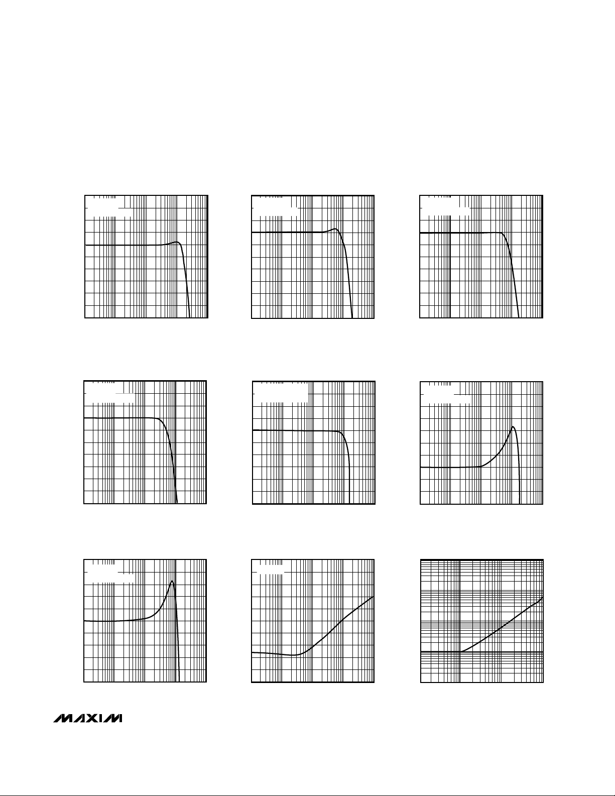
4
-6
100k 1M 10M 100M 1G
MAX4012
SMALL-SIGNAL GAIN vs. FREQUENCY
(A
VCL
= +1)
-4
MAX4012-01
FREQUENCY (Hz)
GAIN (dB)
-2
0
2
3
-5
-3
-1
1
A
VCL
= +1
V
OUT
= 20mVp-p
3
-7
100k 1M 10M 100M 1G
MAX4016/18/20
SMALL-SIGNAL GAIN vs. FREQUENCY
(A
VCL
= +1)
-5
MAX4012-02
FREQUENCY (Hz)
GAIN (dB)
-3
-1
1
2
-6
-4
-2
0
A
VCL
= +1
V
OUT
= 20mVp-p
9
-1
100k 1M 10M 100M 1G
MAX4012
SMALL-SIGNAL GAIN vs. FREQUENCY
(A
VCL
= +2)
1
MAX4012-03
FREQUENCY (Hz)
GAIN (dB)
3
5
7
8
0
2
4
6
A
VCL
= +2
V
OUT
= 20mVp-p
9
-1
100k 1M 10M 100M 1G
MAX4016/18/20
SMALL-SIGNAL GAIN vs. FREQUENCY
(A
VCL
= +2)
1
MAX4012-04
FREQUENCY (Hz)
GAIN (dB)
3
5
7
8
0
2
4
6
A
VCL
= +2
V
OUT
= 20mVp-p
0.5
-0.5
0.1M 1M 10M 100M 1G
MAX4016/18/20
GAIN FLATNESS vs. FREQUENCY
-0.3
MAX4012-07
FREQUENCY (Hz)
GAIN (dB)
-0.1
0.1
0.3
0.4
-0.4
-0.2
0
0.2
A
VCL
= +1
V
OUT
= 20mVp-p
4
-6
100k 1M 10M 100M 1G
LARGE-SIGNAL GAIN vs. FREQUENCY
-4
MAX4012-05
FREQUENCY (Hz)
GAIN (dB)
-2
0
2
3
-5
-3
-1
1
V
OUT
= 2Vp-p
V
OUT BIAS
= 1.75V
0.7
-0.3
0.1M 1M 10M 100M 1G
MAX4012
GAIN FLATNESS vs. FREQUENCY
-0.1
MAX4012-06
FREQUENCY (Hz)
GAIN (dB)
0.1
0.3
0.5
0.6
-0.2
0
0.2
0.4
A
VCL
= +1
V
OUT
= 20mVp-p
50
-150
100k 1M 10M 100M 1G
MAX4016/18/20
CROSSTALK vs. FREQUENCY
-110
MAX4212-08
FREQUENCY (Hz)
CROSSTALK (dB)
-70
-30
10
30
-130
-90
-50
-10
RS = 50Ω
1000
0.1
0.1M 1M 10M 100M
CLOSED-LOOP OUTPUT IMPEDANCE
vs. FREQUENCY
MAX4012-09
FREQUENCY (Hz)
IMPEDANCE (Ω)
100
1
10
__________________________________________Typical Operating Characteristics
(VCC= +5V, VEE= 0V, A
VCL
= +1, RF= 24Ω, RL= 100Ω to VCC/ 2, TA = +25°C, unless otherwise noted.)
MAX4012/MAX4016/MAX4018/MAX4020
Low-Cost, High-Speed, SOT23, Single-Supply
Op Amps with Rail-to-Rail Outputs
6 _______________________________________________________________________________________
0
-100
100k 1M 10M 100M
HARMONIC DISTORTION
vs. FREQUENCY (A
VCL
= +1)
-80
MAX4012-10
FREQUENCY (Hz)
HARMONIC DISTORTION (dBc)
-60
-40
-20
-10
-90
-70
-50
-30
V
OUT
= 2Vp-p
A
VCL
= +1
2ND HARMONIC
3RD HARMONIC
0
-100
100k 1M 10M 100M
HARMONIC DISTORTION
vs. FREQUENCY (A
VCL
= +2)
-80
MAX4012-11
FREQUENCY (Hz)
HARMONIC DISTORTION (dBc)
-60
-40
-20
-10
-90
-70
-50
-30
V
OUT
= 2Vp-p
A
VCL
= +2
2ND HARMONIC
3RD HARMONIC
0
-100
100k 1M 10M 100M
HARMONIC DISTORTION
vs. FREQUENCY (A
VCL
= +5)
-80
MAX4012-12
FREQUENCY (Hz)
HARMONIC DISTORTION (dBc)
-60
-40
-20
-10
-90
-70
-50
-30
V
OUT
= 2Vp-p
A
VCL
= +5
2ND HARMONIC
3RD
HARMONIC
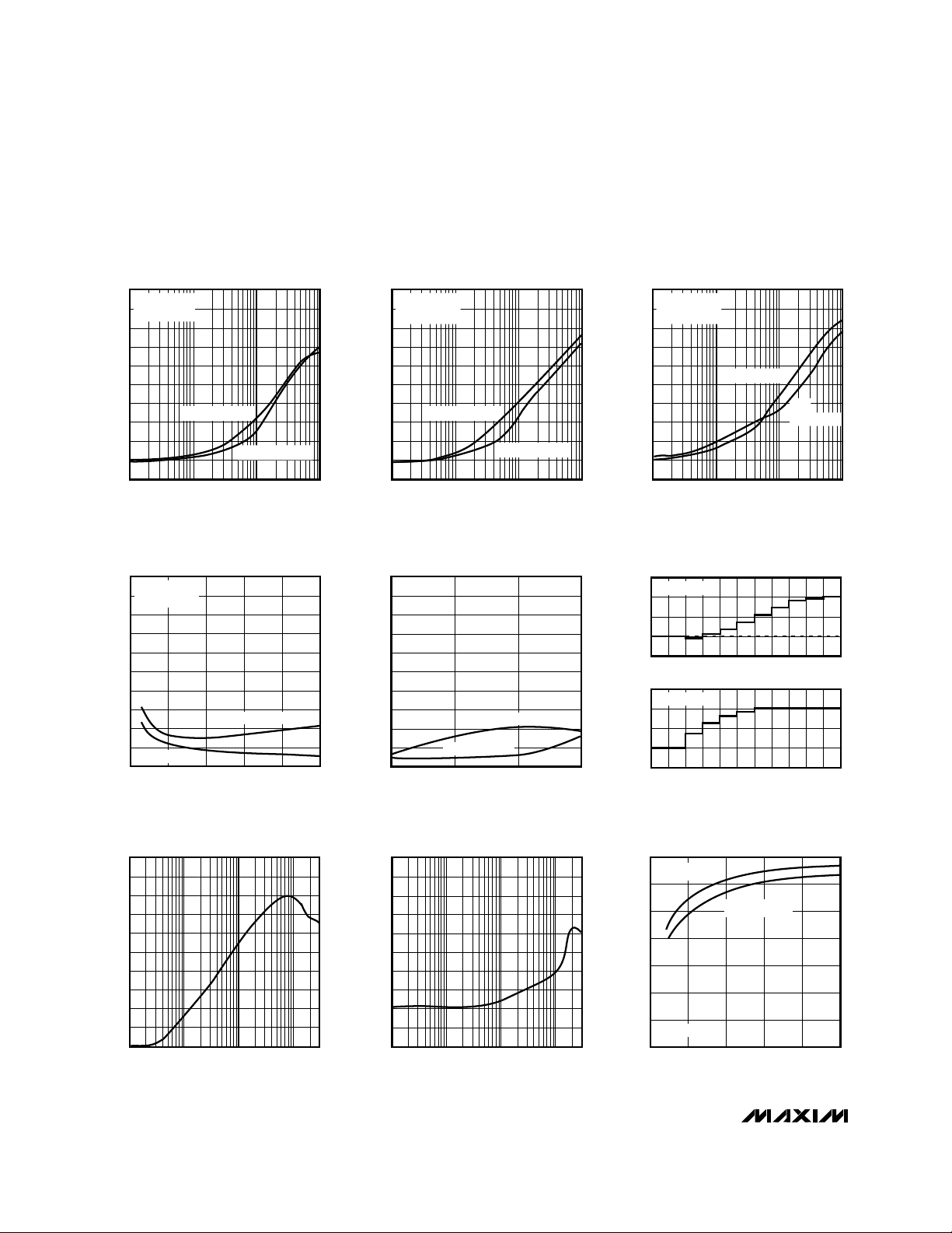
0
-10
-20
-30
-60
-70
-90
-80
-40
-50
-100
MAX4012-13
LOAD (Ω)
0 200 400 600 800 1000
HARMONIC DISTORTION
vs. LOAD
HARMONIC DISTORTION (dBc)
f = 5MHz
V
OUT
= 2Vp-p
3rd HARMONIC
2rd HARMONIC
0
-100
100k 1M 10M 100M
COMMON-MODE REJECTION
vs. FREQUENCY
-80
MAX4012-16
FREQUENCY (Hz)
CMR (dB)
-60
-40
-20
-10
-90
-70
-50
-30
0
-10
-20
-30
-60
-70
-90
-80
-40
-50
-100
MAX4012-14
OUTPUT SWING (Vp-p)
0.5
1.0
1.5 2.0
HARMONIC DISTORTION
vs. OUTPUT SWING
HARMONIC DISTORTION (dBc)
fO = 5MHz
3RD HARMONIC
2ND HARMONIC
-0.01
0 100
0 100
DIFFERENTIAL GAIN AND PHASE
-0.01
0.00
0.00
0.01
0.01
0.02
0.02
0.03
0.03
IRE
IRE
DIFF. PHASE (deg)
DIFF. GAIN (%)
MAX4012-15
VCM = +1.35V
VCM = +1.35V
20
-80
100k 1M 10M 100M
POWER-SUPPLY REJECTION
vs. FREQUENCY
-60
MAX4012-17
FREQUENCY (Hz)
POWER-SUPPLY REJECTION (dB)
-40
-20
0
10
-70
-50
-30
-10
4.5
4.0
3.5
2.5
2.0
1.5
3.0
1.0
MAX4012-18
LOAD RESISTANCE (Ω)
25 50 75 100 125 150
OUTPUT SWING
vs. LOAD RESISTANCE
OUTPUT SWING (Vp-p)
A
VCL
= +2
RL to VCC/2
RL to GROUND
____________________________Typical Operating Characteristics (continued)
(VCC= +5V, VEE= 0V, A
VCL
= +1, RF= 24Ω, RL= 100Ω to VCC/ 2, TA = +25°C, unless otherwise noted.)
MAX4012/MAX4016/MAX4018/MAX4020
Low-Cost, High-Speed, SOT23, Single-Supply
Op Amps with Rail-to-Rail Outputs
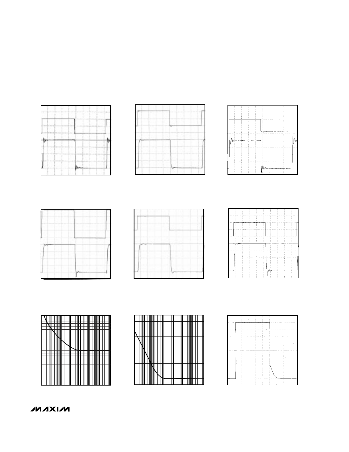
_______________________________________________________________________________________ 7
IN
(50mV/
div)
OUT
(25mV/
div)
VOLTAGE
SMALL-SIGNAL PULSE RESPONSE
(A
VCL
= +1)
MAX4012-19
TIME (20ns/div)
V
CM
= +2.5V, RL = 100Ω to GROUND
IN
(25mV/
div)
OUT
(25mV/
div)
VOLTAGE
SMALL-SIGNAL PULSE RESPONSE
(A
VCL
= +2)
MAX4012-20
TIME (20ns/div)
VCM = +1.25V, RL = 100Ω to GROUND
IN
(50mV/
div)
OUT
(25mV/
div)
VOLTAGE
SMALL-SIGNAL PULSE RESPONSE
(C
L
= 5pF, A
VCL
= +1)
MAX4012-21
TIME (20ns/div)
V
CM
= +1.75V, RL = 100Ω to GROUND
IN
(1V/div)
OUT
(1V/div)
VOLTAGE
LARGE-SIGNAL PULSE RESPONSE
(A
VCL
= +1)
MAX4012-22
TIME (20ns/div)
V
CM
= +1.75V, RL = 100Ω to GROUND
100
10
1
1 10 1k 10M1M
VOLTAGE-NOISE DENSITY
vs. FREQUENCY
MAX4012-25
FREQUENCY (Hz)
NOISE (nV/√Hz)
100 10k 100k
IN
(500mV/
div)
OUT
(500mV/
div)
VOLTAGE
LARGE-SIGNAL PULSE RESPONSE
(A
VCL
= +2)
MAX4012-23
TIME (20ns/div)
V
CM
= 0.9V, RL = 100Ω to GROUND
IN
(1V/
div)
OUT
(500mV/
div)
VOLTAGE
LARGE-SIGNAL PULSE RESPONSE
(C
L
= 5pF, A
VCL
= +2)
MAX4012-24
TIME (20ns/div)
V
CM
= +1.75V, RL = 100Ω to GROUND
10
1
1 10 1k 10M1M
CURRENT-NOISE DENSITY
vs. FREQUENCY
MAX4012-26
FREQUENCY (Hz)
NOISE (pA/√Hz)
100 10k 100k
EN_
5.0V
(ENABLE)
0V
(DISABLE)
1V
0V
OUT
ENABLE RESPONSE TIME
MAX4012-27
TIME (1µs/div)
VIN = +1.0V
____________________________Typical Operating Characteristics (continued)
(VCC= +5V, VEE= 0V, A
VCL
= +1, RF= 24Ω, RL= 100Ω to VCC/ 2, TA = +25°C, unless otherwise noted.)

MAX4012/MAX4016/MAX4018/MAX4020
Low-Cost, High-Speed, SOT23, Single-Supply
Op Amps with Rail-to-Rail Outputs
8 _______________________________________________________________________________________
70
50
60
40
30
20
MAX4012-28
LOAD RESISTANCE (Ω)
0 200 400 600 800 1k
OPEN-LOOP GAIN
vs. LOAD RESISTANCE
OPEN-LOOP GAIN (dB)
400
350
300
250
150
50
100
200
0
MAX4012-29
LOAD RESISTANCE (Ω)
1000 200 500400300 600
CLOSED-LOOP BANDWIDTH
vs. LOAD RESISTANCE
CLOSED-LOOP BANDWIDTH (MHz)
10
-90
100k 10M 100M1M
OFF ISOLATION vs. FREQUENCY
-80
MAX4012-30
FREQUENCY (Hz)
OFF ISOLATION (dB)
-70
-60
-50
-40
-30
-20
-10
0
7
6
4
5
3
MAX4012-31
TEMPERATURE (°C)
-25-50 0 755025 100
SUPPLY CURRENT
vs. TEMPERATURE
SUPPLY CURRENT (mA)
10
8
6
4
2
0
MAX4012-34
SUPPLY VOLTAGE (V)
43 5 6 7 8 9 10 11
SUPPLY CURRENT
vs. SUPPLY VOLTAGE
SUPPLY CURRENT (mA)
6.0
5.5
4.5
5.0
4.0
MAX4012-32
TEMPERATURE (°C)
-25-50 0 755025 100
INPUT BIAS CURRENT
vs. TEMPERATURE
INPUT BIAS CURRENT (µA)
0.20
0.16
0.12
0.04
0.08
0
MAX4012-33
TEMPERATURE (°C)
-25-50 0 755025 100
INPUT OFFSET CURRENT
vs. TEMPERATURE
INPUT OFFSET CURRENT (µA)
5
4
3
1
2
0
MAX4012-35
TEMPERATURE (°C)
-25-50 0 755025 100
INPUT OFFSET VOLTAGE
vs. TEMPERATURE
INPUT OFFSET VOLTAGE (mV)
5.0
4.8
4.6
4.2
4.4
4.0
MAX4012-36
TEMPERATURE (°C)
-25-50 0 755025 100
OUTPUT VOLTAGE SWING
vs. TEMPERATURE
VOLTAGE SWING (Vp-p)
RL = 150Ω TO V
CC
/ 2
____________________________Typical Operating Characteristics (continued)
(VCC= +5V, VEE= 0V, A
VCL
= +1, RF= 24Ω, RL= 100Ω to VCC/ 2, TA = +25°C, unless otherwise noted.)

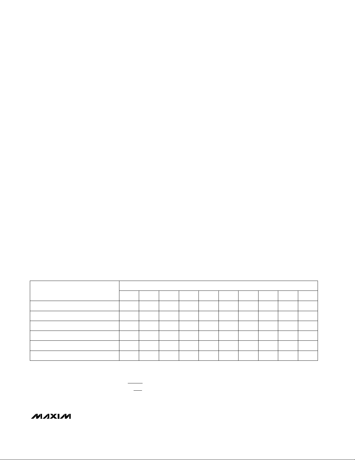
PIN
MAX4012/MAX4016/MAX4018/MAX4020
Low-Cost, High-Speed, SOT23, Single-Supply
Op Amps with Rail-to-Rail Outputs
_______________________________________________________________________________________ 9
______________________________________________________________Pin Description
Amplifier A Noninverting Input—
Amplifier B Output—
Amplifier B Inverting Input—
Amplifier B Noninverting Input—
Amplifier C Output—
Inverting Input4
Positive Power Supply5
Amplifier A Output—
Amplifier A Inverting Input—
Noninverting Input3
Negative Power Supply or Ground (in
single-supply operation)
2
Amplifier Output1
No Connect. Not internally connected.
Tie to ground or leave open.
—
FUNCTION
3
7
6
5
8
—
4
1
2
—
11
—
—
3
7
6
5
—
—
8
1
2
—
4
—
—
5
10
11
12
16
—
4
7
6
—
13
—
8, 9
5
8
9
10
14
—
4
7
6
—
11
—
—
3
7
6
5
10
—
4
1
2
—
13
—
8, 9
INA+
OUTB
INB-
INB+
OUTC
IN-
V
CC
OUTA
INA-
IN+
V
EE
OUT
N.C.
NAME
Amplifier C Inverting Input— 9— 1513 11 INCAmplifier C Noninverting Input— 10— 1412 12 INC+
Amplifier D Output— 14— —— 16 OUTD
Amplifier D Inverting Input— 13— —— 15 INDAmplifier D Noninverting Input— 12— —— 14 IND+
Enable Amplifier— —— —— — EN
Enable Amplifier A— —— 11 — ENA
Enable Amplifier B— —— 33 — ENB
Enable Amplifier C— —— 22 — ENC
MAX4012
SOT23-5
MAX4020
MAX4016
SO/µMAX
MAX4018
SO QSOP SO QSOP
PIN

MAX4012/MAX4016/MAX4018/MAX4020
_______________Detailed Description
The MAX4012/MAX4016/MAX4018/MAX4020 are single-supply, rail-to-rail, voltage-feedback amplifiers that
employ current-feedback techniques to achieve
600V/µs slew rates and 200MHz bandwidths. Excellent
harmonic distortion and differential gain/phase performance make these amplifiers an ideal choice for a wide
variety of video and RF signal-processing applications.
The output voltage swing comes to within 50mV of each
supply rail. Local feedback around the output stage
assures low open-loop output impedance to reduce
gain sensitivity to load variations. This feedback also
produces demand-driven current bias to the output
transistors for ±120mA drive capability, while constraining total supply current to less than 7mA. The input
stage permits common-mode voltages beyond the negative supply and to within 2.25V of the positive supply rail.
__________Applications Information
Choosing Resistor Values
Unity-Gain Configuration
The MAX4012/MAX4016/MAX4018/MAX4020 are internally compensated for unity gain. When configured for
unity gain, the devices require a 24Ω resistor (RF) in
series with the feedback path. This resistor improves
AC response by reducing the Q of the parallel LC cir-
cuit formed by the parasitic feedback capacitance and
inductance.
Inverting and Noninverting Configurations
Select the gain-setting feedback (RF) and input (RG)
resistor values to fit your application. Large resistor values increase voltage noise and interact with the amplifier’s input and PC board capacitance. This can
generate undesirable poles and zeros and decrease
bandwidth or cause oscillations. For example, a noninverting gain-of-two configuration (RF= RG) using 1kΩ
resistors, combined with 1pF of amplifier input capacitance and 1pF of PC board capacitance, causes a pole
at 159MHz. Since this pole is within the amplifier bandwidth, it jeopardizes stability. Reducing the 1kΩ resistors to 100Ω extends the pole frequency to 1.59GHz,
but could limit output swing by adding 200Ω in parallel
with the amplifier’s load resistor. Table 1 shows suggested feedback, gain resistors, and bandwidth for
several gain values in the configurations shown in
Figures 1a and 1b.
Layout and Power-Supply Bypassing
These amplifiers operate from a single +3.3V to +11V
power supply or from dual supplies to ±5.5V. For singlesupply operation, bypass VCCto ground with a 0.1µF
capacitor as close to the pin as possible. If operating with
dual supplies, bypass each supply with a 0.1µF capacitor.
Low-Cost, High-Speed, SOT23, Single-Supply
Op Amps with Rail-to-Rail Outputs
10 ______________________________________________________________________________________
IN
R
G
V
OUT
= [1+ (RF / RG)] V
IN
R
F
R
TO
R
TIN
R
O
V
OUT
MAX40_ _
Figure 1a. Noninverting Gain Configuration Figure 1b. Inverting Gain Configuration
MAX40_ _
V
R
F
= -(RF / RG) V
OUT
R
IN
R
TIN
G
R
S
R
TO
IN
V
OUT
R
O
Maxim recommends using microstrip and stripline techniques to obtain full bandwidth. To ensure that the PC
board does not degrade the amplifier’s performance,
design it for a frequency greater than 1GHz. Pay careful attention to inputs and outputs to avoid large parasitic capacitance. Whether or not you use a constantimpedance board, observe the following guidelines
when designing the board:
• Don’t use wire-wrap boards because they are too
inductive.
• Don’t use IC sockets because they increase parasitic
capacitance and inductance.
• Use surface-mount instead of through-hole components for better high-frequency performance.
• Use a PC board with at least two layers; it should be
as free from voids as possible.
• Keep signal lines as short and as straight as possible. Do not make 90° turns; round all corners.
Rail-to-Rail Outputs,
Ground-Sensing Input
The input common-mode range extends from
(VEE- 200mV) to (VCC- 2.25V) with excellent commonmode rejection. Beyond this range, the amplifier output
is a nonlinear function of the input, but does not undergo phase reversal or latchup.
The output swings to within 60mV of either powersupply rail with a 2kΩ load. The input ground-sensing
and the rail-to-rail output substantially increase the
dynamic range. With a symmetric input in a single +5V
application, the input can swing 2.95Vp-p, and the output can swing 4.9Vp-p with minimal distortion.
Enable Input and Disabled Output
The enable feature (EN_) allows the amplifier to be
placed in a low-power, high-output-impedance state.
Typically, the EN_ logic low input current (IIL) is small.
However, as the EN voltage (VIL) approaches the negative supply rail, IILincreases (Figure 2). A single resistor connected as shown in Figure 3 prevents the rise in
the logic-low input current. This resistor provides a
feedback mechanism that increases VILas the logic
input is brought to VEE. Figure 4 shows the resulting
input current (IIL).
When the MAX4018 is disabled, the amplifier’s output
impedance is 35kΩ. This high resistance and the low
2pF output capacitance make this part ideal in
RF/video multiplexer or switch applications. For larger
arrays, pay careful attention to capacitive loading. See
the
Output Capacitive Loading and Stability
section for
more information.
MAX4012/MAX4016/MAX4018/MAX4020
Low-Cost, High-Speed, SOT23, Single-Supply
Op Amps with Rail-to-Rail Outputs
______________________________________________________________________________________ 11
RF(Ω)
24 500
RG(Ω)
∞
500
COMPONENT
RS(Ω)
— 0
R
TIN
(Ω)
49.9 56
Small-Signal -3dB Bandwidth (MHz) 200 90
RTO(Ω)
49.9 49.9
Table 1. Recommended Component Values
Note: RL= RO+ RTO; R
TIN
and RTOare calculated for 50Ω applications. For 75Ω systems, RTO= 75Ω; calculate R
TIN
from the
following equation:
500
500
—
49.9
105
49.9
500
250
0
62
60
49.9
500
124
—
49.9
25
49.9
500
100
0
100
33
49.9
500
56
—
49.9
11
49.9
500
50
0
∞
25
49.9
500
20
—
49.9
6
49.9
GAIN (V/V)
1200
50
0
∞
10
49.9
+1 -1 +2 -2 +5 -5 +10 -10 +25 -25
R =
TIN
75
75
1-
R
G
Ω

MAX4012/MAX4016/MAX4018/MAX4020
To implement the mux function, the outputs of multiple
amplifiers can be tied together, and only the amplifier
with the selected input will be enabled. All of the other
amplifiers will be placed in the low-power shutdown
mode, with their high output impedance presenting
very little load to the active amplifier output. For gains
of +2 or greater, the feedback network impedance of
all the amplifiers used in a mux application must be
considered when calculating the total load on the
active amplifier output
Output Capacitive Loading and Stability
The MAX4012/MAX4016/MAX4018/MAX4020 are optimized for AC performance. They are not designed to
drive highly reactive loads, which decreases phase
margin and may produce excessive ringing and oscillation. Figure 5 shows a circuit that eliminates this problem. Figure 6 is a graph of the optimal isolation resistor
(RS) vs. capacitive load. Figure 7 shows how a capacitive load causes excessive peaking of the amplifier’s
frequency response if the capacitor is not isolated from
the amplifier by a resistor. A small isolation resistor
(usually 20Ω to 30Ω) placed before the reactive load
prevents ringing and oscillation. At higher capacitive
loads, AC performance is controlled by the interaction
of the load capacitance and the isolation resistor.
Figure 8 shows the effect of a 27Ω isolation resistor on
closed-loop response.
Coaxial cable and other transmission lines are easily
driven when properly terminated at both ends with their
characteristic impedance. Driving back-terminated
transmission lines essentially eliminates the line’s
capacitance.
Low-Cost, High-Speed, SOT23, Single-Supply
Op Amps with Rail-to-Rail Outputs
12 ______________________________________________________________________________________
OUT
IN-
EN_
IN+
10k
ENABLE
MAX40_ _
Figure 2. Enable Logic-Low Input Current vs. V
IL
Figure 4. Enable Logic-Low Input Current vs. V
IL
with 10k
Ω
Series Resistor
Figure 3. Circuit to Reduce Enable Logic-Low Input Current
20
0
-20
-40
-60
-80
-100
INPUT CURRENT (µA)
-120
-140
-160
0 50 100 150 300 350 500
0
-1
-2
-3
-4
-5
-6
INPUT CURRENT (µA)
-7
-8
-9
-10
0 50 100 150 300 350 500
200 250 400 450
mV ABOVE V
200 250 400 450
mV ABOVE V
EE
EE

MAX4012/MAX4016/MAX4018/MAX4020
Low-Cost, High-Speed, SOT23, Single-Supply
Op Amps with Rail-to-Rail Outputs
______________________________________________________________________________________ 13
R
G
R
F
R
ISO
50Ω
C
L
V
OUT
V
IN
R
TIN
MAX40_ _
Figure 5. Driving a Capacitive Load through an Isolation Resistor
30
25
20
5
10
15
0
CAPACITIVE LOAD (pF)
500 100 200150 250
ISOLATION RESISTANCE, R
ISO
(Ω)
Figure 6. Capacitive Load vs. Isolation Resistance
6
-4
100k 10M 100M1M 1G
-2
FREQUENCY (Hz)
GAIN (dB)
0
2
4
5
-3
-1
1
3
CL = 10pF
CL = 15pF
CL = 5pF
Figure 7. Small-Signal Gain vs. Frequency with Load
Capacitance and No Isolation Resistor
3
-7
100k 10M 100M1M 1G
-5
FREQUENCY (Hz)
GAIN (dB)
-3
-1
1
2
-6
-4
-2
0
CL = 68pF
R
ISO
= 27Ω
CL = 120pF
CL = 47pF
Figure 8. Small-Signal Gain vs. Frequency with Load
Capacitance and 27
Ω
Isolation Resistor

MAX4012/MAX4016/MAX4018/MAX4020
Low-Cost, High-Speed, SOT23, Single-Supply
Op Amps with Rail-to-Rail Outputs
14 ______________________________________________________________________________________
TOP VIEW
14
13
12
11
10
9
8
1
2
3
4
5
6
7
OUTC
INC-
INC+
V
EE
V
CC
ENB
ENC
ENA
MAX4018
INB+
INBOUTB
OUTA
INA-
INA+
SO
14
13
12
11
10
9
8
1
2
3
4
5
6
7
OUTD
IND-
IND+
V
EE
V
CC
INA+
INA-
OUTA
MAX4020
INC+
INCOUTC
OUTB
INB-
INB+
SO
16
15
14
13
12
11
10
9
1
2
3
4
5
6
7
8
OUTC
INCINC+
V
EE
INB+
INBOUTB
N.C.
ENA
ENC
ENB
V
CC
INA+
INA-
OUTA
N.C.
MAX4018
QSOP
16
15
14
13
12
11
10
9
1
2
3
4
5
6
7
8
OUTD
INDIND+
V
EE
INC+
INCOUTC
N.C.
OUTA
INA-
INA+
V
CC
INB+
INB-
OUTB
N.C.
MAX4020
QSOP
INB-
INB+
V
EE
1
2
8
7
V
CC
OUTB
INA-
INA+
OUTA
SO/µMAX
3
4
6
5
MAX4016
_____________________________________________Pin Configurations (continued)
MAX4012/MAX4016/MAX4018/MAX4020
Low-Cost, High-Speed, SOT23, Single-Supply
Op Amps with Rail-to-Rail Outputs
______________________________________________________________________________________ 15
362MAX4020
299MAX4018
190MAX4016
95MAX4012
TRANSISTOR
COUNT
PART
___________________Chip Information_Ordering Information (continued)
PART
TEMP.
RANGE
SOT
TOP
MARK
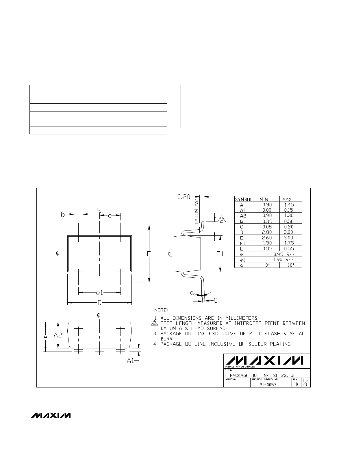
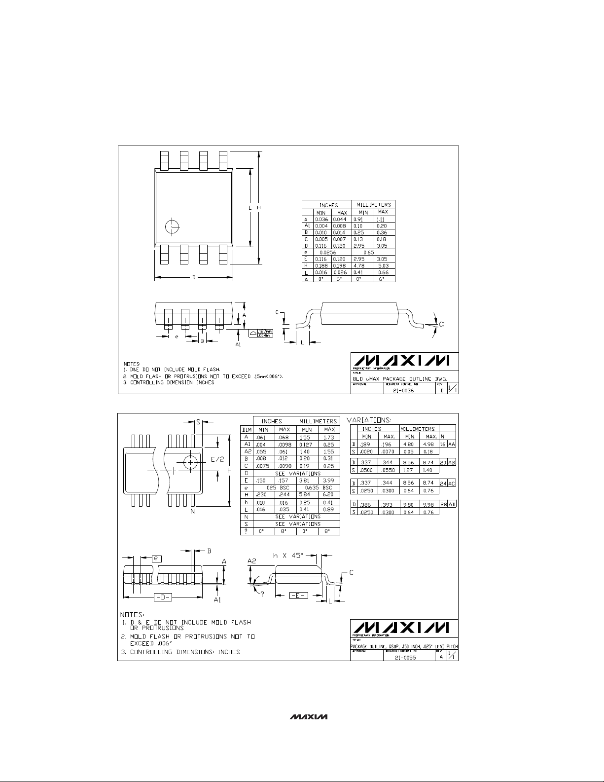
________________________________________________________Package Information
PIN-
PACKAGE
14 SO
16 QSOP
14 SO
16 QSOP
MAX4018ESD
-40°C to +85°C
MAX4018EEE -40°C to +85°C
MAX4020ESD
-40°C to +85°C
MAX4020EEE -40°C to +85°C
—
—
—
—
SOT5L.EPS
Maxim cannot assume responsibility for use of any circuitry other than circuitry entirely embodied in a Maxim product. No circuit patent licenses are
implied. Maxim reserves the right to change the circuitry and specifications without notice at any time.
16
____________________Maxim Integrated Products, 120 San Gabriel Drive, Sunnyvale, CA 94086 408-737-7600
© 1997 Maxim Integrated Products Printed USA is a registered trademark of Maxim Integrated Products.
MAX4012/MAX4016/MAX4018/MAX4020
Low-Cost, High-Speed, SOT23, Single-Supply
Op Amps with Rail-to-Rail Outputs
___________________________________________Package Information (continued)
8LUMAXD.EPS
QSOP.EPS
 Loading...