

_______________General Description
The MAX4014/MAX4017/MAX4019/MAX4022 are precision, closed-loop, gain of +2 (or -1) buffers featuring
high slew rates, high output current drive, and low differential gain and phase errors. These single-supply
devices operate from +3.15V to +11V, or from ±1.575V
to ±5.5V dual supplies. The input voltage range extends
100mV beyond the negative supply rail and the outputs
swing Rail-to-Rail®.
These devices require only 5.5mA of quiescent supply
current while achieving a 200MHz -3dB bandwidth and
a 600V/µs slew rate. In addition, the MAX4019 has a
disable feature that reduces the supply current to
400µA. Input voltage noise for these parts is only
10nV/√Hz and input current noise is only 1.3pA/√Hz.
This buffer family is ideal for low-power/low-voltage
applications that require wide bandwidth, such as
video, communications, and instrumentation systems.
For space-sensitive applications, the MAX4014 comes
in a tiny 5-pin SOT23 package.
________________________Applications
Portable/Battery-Powered Instruments
Video Line Driver
Analog-to-Digital Converter Interface
CCD Imaging Systems
Video Routing and Switching Systems
____________________________Features
♦ Internal Precision Resistors for Closed-Loop
Gains of +2 or -1
♦ High Speed:
200MHz -3dB Bandwidth
30MHz 0.1dB Gain Flatness (6MHz min)
600V/µs Slew Rate
♦ Single 3.3V/5.0V Operation
♦ Outputs Swing Rail-to-Rail
♦ Input Voltage Range Extends Beyond V
EE
♦ Low Differential Gain/Phase: 0.04%/0.02°
♦ Low Distortion at 5MHz:
-78dBc Spurious-Free Dynamic Range
-75dB Total Harmonic Distortion
♦ High Output Drive: ±120mA
♦ Low, 5.5mA Supply Current
♦ 400µA Shutdown Supply Current
♦ Space-Saving SOT23-5, µMAX, or QSOP Packages
For free samples & the latest literature: http://www.maxim-ic.com, or phone 1-800-998-8800.
For small orders, phone 408-737-7600 ext. 3468.
MAX4014/MAX4017/MAX4019/MAX4022
Low-Cost, High-Speed, Single-Supply, Gain of +2
Buffers with Rail-to-Rail Outputs in SOT23
________________________________________________________________
Maxim Integrated Products
1
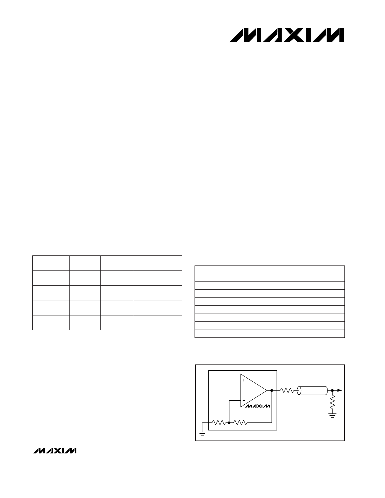
__________Typical Operating Circuit
19-1284; Rev 0; 10/97
______________Ordering Information
PART
NO. OF
AMPS
ENABLE PIN-PACKAGE
MAX4014 1 No 5-Pin SOT23
MAX4017 2 No 8-Pin SO/µMAX
MAX4019 3 Yes
14-Pin SO,
16-Pin QSOP
MAX4022 4 No
14-Pin SO,
16-Pin QSOP
_____________________Selector Guide
PART
SOT
TOP MARK
MAX4014EUK
ABZQ
TEMP. RANGE
PIN-
PACKAGE
-40°C to +85°C 5 SOT23-5
MAX4017ESA
—-40°C to +85°C 8 SO
MAX4017EUA —-40°C to +85°C 8 µMAX
MAX4019ESD
—-40°C to +85°C 14 SO
MAX4019EEE —-40°C to +85°C 16 QSOP
MAX4022ESD
—
MAX4022EEE —
-40°C to +85°C 14 SO
-40°C to +85°C 16 QSOP
MAX4014
75Ω
500Ω
GAIN OF +2 VIDEO/RF CABLE DRIVER
500Ω
V
OUT
IN-
IN+
75Ω
Rail-to-Rail is a registered trademark of Nippon Motorola Ltd.
MAX4014/MAX4017/MAX4019/MAX4022
Low-Cost, High-Speed, Single-Supply, Gain of +2
Buffers with Rail-to-Rail Outputs in SOT23
2 _______________________________________________________________________________________
ABSOLUTE MAXIMUM RATINGS
DC ELECTRICAL CHARACTERISTICS
(VCC= +5V, VEE= 0V, IN_- =0V, EN_ = 5V, RL= ∞ to ground, V
OUT
= VCC/ 2, noninverting configuration, TA= T
MIN
to T
MAX
, unless
otherwise noted. Typical values are at T
A
= +25°C.) (Note 1)
Supply Voltage (V
CC
to VEE)..................................................12V
IN_-, IN_+, OUT_, EN_ ....................(V
EE
- 0.3V) to (VCC+ 0.3V)
Output Short-Circuit Duration to V
CC
or VEE..............Continuous
Continuous Power Dissipation (T
A
= +70°C)
5-pin SOT23 (derate 7.1mW/°C above+70°C)..............571mW
8-pin SO (derate 5.9mW/°C above +70°C)...................471mW
8-pin µMAX (derate 4.1mW/°C above +70°C)..............330mW
14-pin SO (derate 8.3mW/°C above +70°C).................667mW
16-pin QSOP (derate 8.3mW/°C above +70°C)............667mW
Operating Temperature Range ...........................-40°C to +85°C
Storage Temperature Range.............................-65°C to +150°C
Lead Temperature (soldering, 10sec).............................+300°C
Stresses beyond those listed under “Absolute Maximum Ratings” may cause permanent damage to the device. These are stress ratings only, and functional
operation of the device at these or at any other conditions beyond those indicated in the operational sections of the specifications is not implied. Exposure
to absolute maximum rating conditions for extended periods may affect device reliability.
VEN_ Logic-High Threshold V
IH
MAX4019 VCC- 1.5
VEN_ Logic-Low Threshold V
IL
MAX4019 VCC- 2.6
kΩDisabled Output Resistance R
OUT(OFF)
MAX4019, EN_ = 0V, 0V ≤ V
OUT
≤ 5V 1
VOperating Supply-Voltage Range VCCto V
EE
3.15 11.0
dB
Power-Supply Rejection Ratio
(Note 3)
PSRR
VCC= 5V, VEE= 0V, V
OUT
= 2V 46 57
Output Current I
OUT
±80 ±120 mARL= 20Ω to VCCor V
EE
Output Resistance R
OUT
25
mΩ
f = DC
Short-Circuit Output Current I
SC
±150 mASinking or sourcing
VEE-0.1 VCC+0.1IN_-
VOL- V
EE
VCC- V
OH
VOL- V
EE
VCC- V
OH
VOL- V
EE
VCC- V
OH
0.06
0.06
RL= 2kΩ
0.04 0.50
0.75 1.50
RL=150Ω
0.04 0.50
Output Voltage Swing V
OUT
V
1.60 2.00
RL= 50Ω
PARAMETER SYMBOL MIN TYP MAX UNITS
Input Resistance R
IN
3
MΩ
Input Bias Current I
B
5.4 20 µA
Input Offset Voltage Matching ±1 mV
Voltage Gain A
V
1.9 2 2.1 V/V
Input Offset Voltage
Input Voltage Range V
IN
VEE-0.1 VCC-2.25
V
V
OS
4 20 mV
Input Offset Voltage Drift TC
VOS
8 µV/°C
CONDITIONS
IN_+, over input voltage range
IN_+ (Note 2)
Any channels for
MAX4017/MAX4019/MAX4022
RL≥ 50Ω, (VEE+ 0.5V) ≤ V
OUT
≤ (VCC- 2.0V)
IN_+
RL= 50Ω
µAEN_ Logic Input Low Current I
IL
0.5
VCC= 5V, VEE= -5V, V
OUT
= 0V 54 66
VCC= 3.3V, VEE= 0V, V
OUT
= 0.9V 45
MAX4019
(VEE+ 0.2V) ≤ EN_ ≤ V
CC
200 550EN_ = V
EE
µAEN_ Logic Input High Current I
IH
0.5 10MAX4019, EN_ = V
CC
mA
Quiescent Supply Current
(per Buffer)
I
CC
5.5 8.0Enabled (EN_ = V
CC)
0.4 0.7MAX4019, disabled (EN_ = VEE)
MAX4014/MAX4017/MAX4019/MAX4022
Low-Cost, High-Speed, Single-Supply, Gain of +2
Buffers with Rail-to-Rail Outputs in SOT23
_______________________________________________________________________________________ 3
Note 1: The MAX4014EUK is 100% production tested at TA= +25°C. Specifications over temperature limits are guaranteed by
design.
Note 2: Tested with V
OUT
= +2.5V.
Note 3: PSRR for single +5V supply tested with V
EE
= 0V, VCC= +4.5V to +5.5V; for dual ±5V supply with VEE= -4.5V to -5.5V,
V
CC
= +4.5V to +5.5V; and for single +3V supply with VEE= 0V, VCC= +3.15V to +3.45V.
Note 4: Guaranteed by design.
AC ELECTRICAL CHARACTERISTICS
(VCC= +5V, VEE= 0V, IN_- = 0V, EN_ = 5V, RL= 100Ω to ground, noninverting configuration, TA= T
MIN
to T
MAX,
unless
otherwise noted. Typical values are at T
A
= +25°C.)
V
OUT
= 20mVp-p
MAX4017/MAX4019/MAX4022,
f = 10MHz, V
OU
T
= 2Vp-p
dB-95X
TALK
Buffer Crosstalk
MAX4017/MAX4019/MAX4022,
f = 10MHz, V
OUT
= 20mVp-p
dB0.1Buffer Gain Matching
MAX4019 µs1t
OFF
Buffer Disable Time
fC= 5MHz, V
OUT
= 2Vp-p dBc-78SFDR
Spurious-Free Dynamic
Range
MAX4019
f = 10MHz
MAX4019, EN_ = 0V
f = 10kHz
f = 10kHz
NTSC, RL= 150Ω
NTSC, RL= 150Ω
fC= 10MHz, A
VCL
= +2V/V
V
OUT
= 2Vp-p,
fC= 5MHz
V
OUT
= 100mVp-p
f = 10.0MHz
V
OUT
= 2V step
V
OUT
= 2V step
V
OUT
= 2Vp-p
V
OUT
= 20mVp-p (Note 4)
CONDITIONS
ns100t
ON
Buffer Enable Time
Ω
6Z
OUT
Output Impedance
pF2C
OUT(OFF)
Disabled Output Capacitance
pF1C
IN
Input Capacitance
pA/√Hz
1.3i
n
Input Noise Current Density
nV/√Hz
10e
n
Input Noise Voltage Density
%0.04DGDifferential Gain Error
degrees0.02DPDifferential Phase Error
dBm11Input 1dB Compression Point
dBm35IP3Third-Order Intercept
-75
-82
HDHarmonic Distortion
MHz200BW
SS
Small-Signal -3dB Bandwidth
-78
ns1tR, t
F
Rise/Fall Time
ns45t
S
Settling Time to 0.1%
V/µs600SRSlew Rate
MHz140BW
LS
Large-Signal -3dB Bandwidth
MHz6 30BW
0.1dB
Bandwidth for 0.1dB Gain
Flatness
UNITSMIN TYP MAXSYMBOLPARAMETER
dBc
Second harmonic
Total harmonic
distortion
Third harmonic
MAX4014/MAX4017/MAX4019/MAX4022
Low-Cost, High-Speed, Single-Supply, Gain of +2
Buffers with Rail-to-Rail Outputs in SOT23
4 _______________________________________________________________________________________
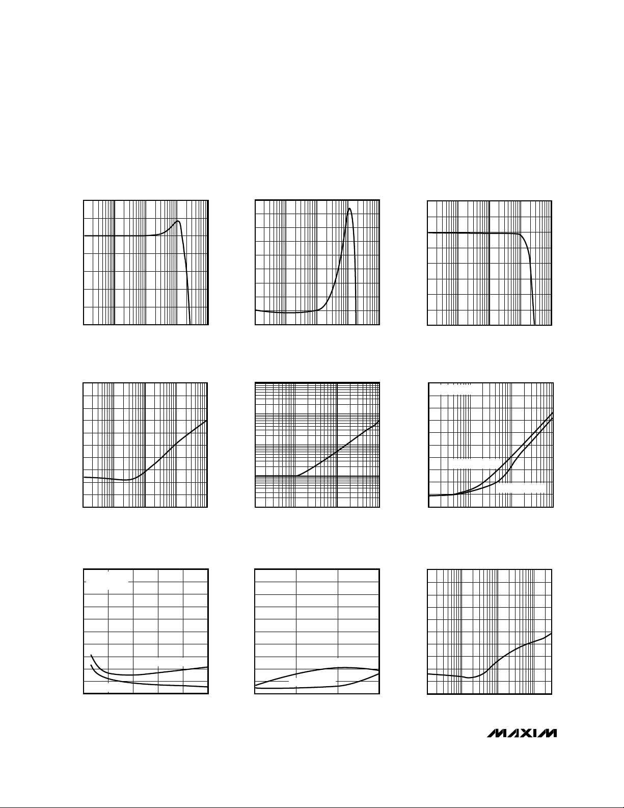
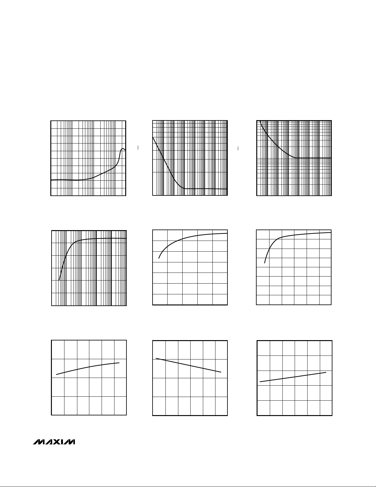
8
1
100k 1M 10M 100M 1G
SMALL-SIGNAL GAIN vs. FREQUENCY
3
MAX4014-01
FREQUENCY (Hz)
GAIN (dB)
5
7
2
4
6
6.8
6.7
5.9
100k 1M 10M 100M 1G
GAIN FLATNESS vs. FREQUENCY
MAX4014-02
FREQUENCY (Hz)
GAIN (dB)
6.0
6.2
6.5
6.6
6.1
6.4
6.3
6
7
8
0
100k 1M 10M 100M 1G
LARGE-SIGNAL GAIN vs. FREQUENCY
3
MAX4014-03
FREQUENCY (Hz)
GAIN (dB)
5
2
1
4
50
-150
100k 1M 10M 100M 1G
MAX4017/19/22
CROSSTALK vs. FREQUENCY
-110
MAX4014-04
FREQUENCY (Hz)
CROSSTALK (dB)
-70
-30
10
30
-130
-90
-50
-10
0
-10
-20
-30
-60
-70
-90
-80
-40
-50
-100
MAX4014-07
LOAD (Ω)
0 200 400 600 800 1000
HARMONIC DISTORTION
vs. LOAD
HARMONIC DISTORTION (dBc)
f = 5MHz
V
OUT
= 2Vp-p
3rd HARMONIC
2rd HARMONIC
1000
0.1
0.1M 1M 10M 100M
CLOSED-LOOP OUTPUT IMPEDANCE
vs. FREQUENCY
MAX4014-05
FREQUENCY (Hz)
IMPEDANCE (Ω)
100
1
10
0
-100
100k 1M 10M 100M
HARMONIC DISTORTION
vs. FREQUENCY
-80
MAX4014-06
FREQUENCY (Hz)
HARMONIC DISTORTION (dBc)
-60
-40
-20
-10
-90
-70
-50
-30
V
OUT
= 2Vp-p
2ND HARMONIC
3RD HARMONIC
0
-10
-20
-30
-60
-70
-90
-80
-40
-50
-100
MAX4014-08
OUTPUT SWING (Vp-p)
0.5
1.0
1.5 2.0
HARMONIC DISTORTION
vs. OUTPUT SWING
HARMONIC DISTORTION (dBc)
f = 5MHz
3RD HARMONIC
2ND HARMONIC
10
-90
100k 10M 100M1M
MAX4019
OFF ISOLATION vs. FREQUENCY
-80
MAX4014-09
FREQUENCY (Hz)
OFF ISOLATION (dB)
-70
-60
-50
-40
-30
-20
-10
0
__________________________________________Typical Operating Characteristics
(VCC= +5V, VEE= 0V, A
VCL
= +2, RL= 150Ω to VCC/ 2, TA = +25°C, unless otherwise noted.)
MAX4014/MAX4017/MAX4019/MAX4022
Low-Cost, High-Speed, Single-Supply, Gain of +2
Buffers with Rail-to-Rail Outputs in SOT23
_______________________________________________________________________________________
5
20
-80
100k 1M 10M 100M
POWER-SUPPLY REJECTION
vs. FREQUENCY
-60
MAX4014-10
FREQUENCY (Hz)
POWER-SUPPLY REJECTION (dB)
-40
-20
0
10
-70
-50
-30
-10
7
6
4
5
3
MAX4014-16
TEMPERATURE (°C)
-25-50 0 755025 100
POWER-SUPPLY CURRENT (PER AMPLIFIER)
vs. TEMPERATURE
POWER-SUPPLY CURRENT (mA)
10
1
1 10 1k 10M1M
CURRENT NOISE DENSITY
vs. FREQUENCY
MAX4014-11
FREQUENCY (Hz)
NOISE (pA/ √Hz)
100 10k 100k
100
10
1
1 10 1k 10M1M
VOLTAGE NOISE DENSITY
vs. FREQUENCY
MAX4014-12
FREQUENCY (Hz)
NOISE (nV/√Hz)
100 10k 100k
5
2
10 100 1k 10k 100k 1M
OUTPUT SWING
vs. LOAD RESISTANCE
MAX4014-13
LOAD RESISTANCE (Ω)
OUTPUT SWING (Vp-p)
3
4
4.5
4.0
3.5
2.5
2.0
1.5
3.0
1.0
MAX4014-14
LOAD RESISTANCE (Ω)
25 50 75 100 125 150
OUTPUT SWING
vs. LOAD RESISTANCE (R
L
)
OUTPUT SWING (Vp-p)
400
350
300
250
150
50
100
200
0
MAX4014-15
LOAD RESISTANCE (Ω)
1000 200 500400300 600
BANDWIDTH
vs. LOAD RESISTANCE
BANDWIDTH (MHz)
6.0
5.5
4.5
5.0
4.0
MAX4014-17
TEMPERATURE (°C)
-25-50 0 755025 100
INPUT BIAS CURRENT
vs. TEMPERATURE
INPUT BIAS CURRENT (µA)
0.20
0.16
0.12
0.04
0.08
0
MAX4014-18
TEMPERATURE (°C)
-25-50 0 755025 100
INPUT OFFSET CURRENT
vs. TEMPERATURE
INPUT OFFSET CURRENT (µA)
__________________________________________Typical Operating Characteristics
(VCC= +5V, VEE= 0V, A
VCL
= +2, RL= 150Ω to VCC/ 2, TA = +25°C, unless otherwise noted.)

MAX4014/MAX4017/MAX4019/MAX4022
Low-Cost, High-Speed, Single-Supply, Gain of +2
Buffers with Rail-to-Rail Outputs in SOT23
6 _______________________________________________________________________________________
10
8
6
4
2
0
MAX4014-19
POWER-SUPPLY VOLTAGE (V)
43 5 6 7 8 9 10 11
POWER-SUPPLY CURRENT (PER AMPLIFIER)
vs. POWER-SUPPLY VOLTAGE
POWER-SUPPLY CURRENT (mA)
5.0
4.8
4.6
4.2
4.4
4.0
MAX4014-21
TEMPERATURE (°C)
-25-50 0 755025 100
VOLTAGE SWING vs. TEMPERATURE
VOLTAGE SWING (Vp-p)
RL = 150Ω TO V
CC
/ 2
5
4
3
1
2
0
MAX4014-20
TEMPERATURE (°C)
-25-50 0 755025 100
INPUT OFFSET VOLTAGE
vs. TEMPERATURE
INPUT OFFSET VOLTAGE (mV)
-0.025
-0.020
-0.015
-0.010
-0.005
0.000
0.005
0.010
0 100
0 100
DIFFERENTIAL GAIN AND PHASE
-0.05
-0.04
-0.02
-0.03
-0.01
0.00
0.01
IRE
IRE
DIFF. PHASE (deg)
DIFF. GAIN (%)
MAX4014-22
IN
OUT
VOLTAGE (500mV/div)
LARGE-SIGNAL PULSE RESPONSE
MAX4014-25
TIME (20ns/div)
V
CM
= 0.9V, RL = 100Ω to GROUND
IN
OUT
VOLTAGE (25mV/div)
SMALL-SIGNAL PULSE RESPONSE
MAX4014-23
TIME (20ns/div)
VCM = 1.25V, RL = 100Ω to GROUND
IN
OUT
VOLTAGE (25mV/div)
SMALL-SIGNAL PULSE RESPONSE
(C
L
= 5pF)
MAX4014-24
TIME (20ns/div)
IN
OUT
VOLTAGE (500mV/div)
LARGE-SIGNAL PULSE RESPONSE
(C
L
= 5pF)
MAX4014-26
TIME (20ns/div)
V
CM
= 1.75V, RL = 100Ω to GROUND
EN_
5.0V
(ENABLE)
0V
(DISABLE)
1V
0V
OUT
ENABLE RESPONSE TIME
MAX4014-27
TIME (1µs/div)
VIN = 0.5V
__________________________________________Typical Operating Characteristics
(VCC= +5V, VEE= 0V, A
VCL
= +2, RL= 150Ω to VCC/ 2, TA = +25°C, unless otherwise noted.)
MAX4014/MAX4017/MAX4019/MAX4022
Low-Cost, High-Speed, Single-Supply, Gain of +2
Buffers with Rail-to-Rail Outputs in SOT23
_______________________________________________________________________________________ 7
______________________________________________________________Pin Description
53—
87—
96—
105—
14——
——4
485
71—
62—
——3
1142
SOT23-5
——1
———
SOSO/µMAX
3——
2——
———
———
———
1——
12——
13——
335
7710
6611
5512
10816
———
444
117
226
———
131113
QSOP
———
8, 9—8, 9
QSOPSO
——3
——2
1614—
1513—
1412—
——1
121014
11915
INA+
OUTB
INB-
INB+
OUTC
IN-
V
CC
OUTA
INA-
IN+
V
EE
OUT
N.C.
ENB
ENC
OUTD
IND-
IND+
ENA
INC+
INC-
Amplifier A Noninverting Input
Amplifier B Output
Amplifier B Inverting Input
Amplifier B Noninverting Input
Amplifier C Output
Inverting Input
Positive Power Supply
Amplifier A Output
Amplifier A Inverting Input
Noninverting Input
Negative Power Supply or Ground
(in single-supply operation)
Amplifier Output
No Connect. Not internally connected. Tie to
ground or leave open.
Enable Input for Amplifier B
Enable Input for Amplifier C
Amplifier D Output
Amplifier D Inverting Input
Amplifier D Noninverting Input
Enable Input for Amplifier A
Amplifier C Noninverting Input
Amplifier C Inverting Input
MAX4014 MAX4017 MAX4019 MAX4022
PIN
NAME FUNCTION
MAX4014/MAX4017/MAX4019/MAX4022
Low-Cost, High-Speed, Single-Supply, Gain of +2
Buffers with Rail-to-Rail Outputs in SOT23
8 _______________________________________________________________________________________
_______________Detailed Description
The MAX4014/MAX4017/MAX4019/MAX4022 are single-supply, rail-to-rail output, voltage-feedback, closedloop buffers that employ current-feedback techniques
to achieve 600V/µs slew rates and 200MHz bandwidths. These buffers use internal 500Ω resistors to
provide a preset closed-loop gain of +2V/V in the noninverting configuration or -1V/V in the inverting configuration. Excellent harmonic distortion and differential
gain/phase performance make these buffers an ideal
choice for a wide variety of video and RF signal-processing applications.
Local feedback around the buffer’ s output stage
ensures low output impedance, which reduces gain
sensitivity to load variations. This feedback also produces demand-driven current bias to the output transistors for ±120mA drive capability, while constraining
total supply current to less than 7mA.
__________Applications Information
Power Supplies
These devices operate from a single +3.15V to +11V
power supply or from dual supplies of ±1.575V to
±5.5V. For single-supply operation, bypass the VCCpin
to ground with a 0.1µF capacitor as close to the pin as
possible. If operating with dual supplies, bypass each
supply with a 0.1µF capacitor.
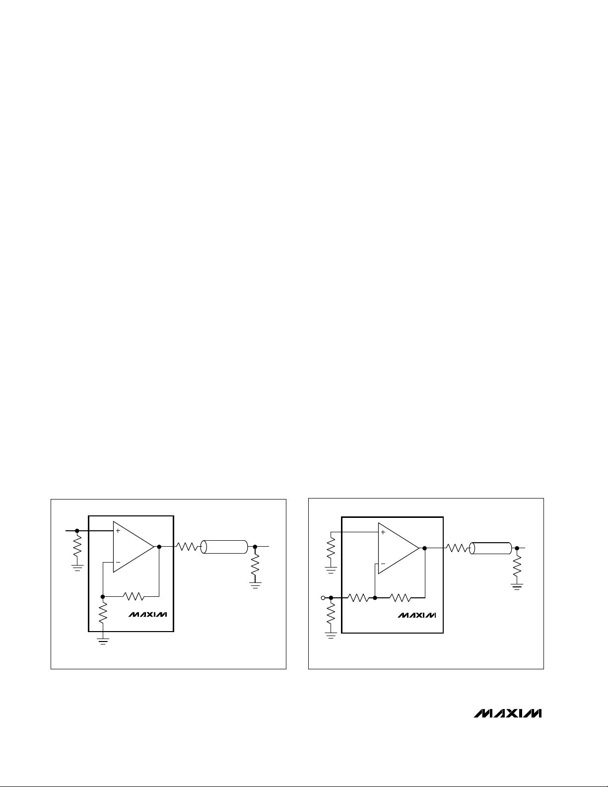
Selecting Gain Configuration
Each buffer in the MAX4014 family can be configured
for a voltage gain of +2V/V or -1V/V. For a gain of
+2V/V, ground the inverting terminal. Use the noninverting terminal as the signal input of the buffer (Figure 1a).
Grounding the noninverting terminal and using the
inverting terminal as the signal input configures the
buffer for a gain of -1V/V (Figure 1b).
Since the inverting input exhibits a 500Ω input impedance, terminate the input with a 56Ω resistor when the
device is configured for an inverting gain in 50Ω applications (terminate with 88Ω in 75Ω applications).
Terminate the input with a 49.9Ω resistor in the noninverting case. Output terminating resistors should directly match cable impedances in either configuration.
Layout Techniques
Maxim recommends using microstrip and stripline techniques to obtain full bandwidth. To ensure that the PC
board does not degrade the buffer’s performance, design
it for a frequency greater than 1GHz. Pay careful attention
to inputs and outputs to avoid large parasitic capacitance. Whether or not you use a constant-impedance
board, observe the following guidelines when designing
the board:
• Don’t use wire-wrapped boards. They are too inductive.
• Don’t use IC sockets. They increase parasitic capacitance and inductance.
• Use surface-mount instead of through-hole components for better high-frequency performance.
• Use a PC board with at least two layers; it should be
as free from voids as possible.
• Keep signal lines as short and as straight as possible. Do not make 90° turns; round all corners.
MAX40_ _
500Ω
500Ω
IN-
OUT
*R
*R
OUT
IN
R
TIN
IN+
*RL = 2R
Figure 1a. Noninverting Gain Configuration (AV= +2V/V) Figure 1b. Inverting Gain Configuration (AV= -1V/V)
IN+
R
S
IN
R
TIN
*R
L
500Ω
IN-
= 2R
500Ω
MAX40_ _
OUT
*R
OUT
*R

MAX4014/MAX4017/MAX4019/MAX4022
Low-Cost, High-Speed, Single-Supply, Gain of +2
Buffers with Rail-to-Rail Outputs in SOT23
_______________________________________________________________________________________ 9
Input Voltage Range and Output Swing
The input range for the MAX4014 family extends from
(VEE- 100mV) to (VCC- 2.25V). Input ground sensing
increases the dynamic range for single-supply applications. The outputs drive a 2kΩ load to within 60mV of
the power-suply rails. With heavier loads, the output
swing is reduced as shown in the
Electrical Character-
istics
and the
Typical Operating Characteristics
. As the
load increases, the input range is effectively limited by
the output-drive capability, since the buffers have a
fixed voltage gain of +2 or -1.
For example, a 50Ω load can typically be driven from
40mV above V
EE
to 1.6V below VCC, or 40mV to 3.4V
when operating from a single +5V supply. If the buffer is
operated in the noninverting, gain of +2 configuration
with the inverting input grounded, the effective input
voltage range becomes 20mV to 1.7V, instead of the
-100mV to 2.75V indicated by the
Electrical Character-
istics
. Beyond the effective input range, the buffer output is a nonlinear function of the input, but it will not
undergo phase reversal or latchup.
Enable
The MAX4019 has an enable feature (EN_) that allows
the buffer to be placed in a low-power state. When the
buffers are disabled, the supply current will not exceed
550µA per buffer.
As the voltage at the EN_ pin approaches the negative
supply rail, the EN_ input current rises. Figure 2 shows
a graph of EN_ input current versus EN_ pin voltage.
Figure 3 shows the addition of an optional resistor in
series with the EN pin, to limit the magnitude of the current increase. Figure 4 displays the resulting EN pin
input current to voltage relationship.
20
-160
0 100 300 500
-100
-120
0
V
IL
(mV ABOVE VEE)
INPUT CURRENT (µA)
200 400
-60
-140
-20
-40
-80
Figure 2. Enable Logic-Low Input Current vs. Enable LogicLow Threshold
OUT
IN-
EN_
IN+
10k
ENABLE
MAX40_ _
500Ω 500Ω
Figure 3. Circuit to Reduce Enable Logic-Low Input Current
0
-10
0 100 300 500
-7
-8
-1
V
IL
(mV ABOVE VEE)
INPUT CURRENT (µA)
200 400
-3
-5
-9
-2
-4
-6
Figure 4. Enable Logic-Low Input Current vs. Enable LogicLow Threshold with 10k
Ω
Series Resistor

MAX4014/MAX4017/MAX4019/MAX4022
Low-Cost, High-Speed, Single-Supply, Gain of +2
Buffers with Rail-to-Rail Outputs in SOT23
10 ______________________________________________________________________________________
Disabled Output Resistance
The MAX4014/MAX4017/MAX4019/MAX4022 include
internal protection circuitry that prevents damage to the
precision input stage from large differential input voltages, as shown in Figure 5. This protection circuitry consists of five back-to-back Schottky diodes between IN_+
and IN_-. These diodes lower the disabled output resistance from 1kΩ to 500Ω when the output voltage is 3V
greater or less than the voltage at IN_+. Under these
conditions, the input protection diodes will be forward
biased, lowering the disabled output resistance to 500Ω.
Output Capacitive Loading and Stability
The MAX4014/MAX4017/MAX4019/MAX4022 provide
maximum AC performance with no load capacitance.
This is the case when the load is a properly terminated
transmission line. However, they are designed to drive
up 25pF of load capacitance without oscillating, but
with reduced AC performance.
Driving large capacitive loads increases the chance of
oscillations occurring in most amplifier circuits. This is
especially true for circuits with high loop gains, such as
voltage followers. The buffer’s output resistance and
the load capacitor combine to add a pole and excess
phase to the loop response. If the frequency of this
pole is low enough to interfere with the loop response
and degrade phase margin sufficiently, oscillations can
occur.
A second problem when driving capacitive loads
results from the amplifier’s output impedance, which
looks inductive at high frequencies. This inductance
forms an L-C resonant circuit with the capacitive load,
which causes peaking in the frequency response and
degrades the amplifier’s gain margin.
Figure 6 shows the frequency response of the MAX4014/
MAX4017/MAX4019/MAX4022 under different capacitive
loads. To drive loads with greater than 25pF of capacitance or to settle out some of the peaking, the output
requires an isolation resistor like the one shown in
MAX4014
MAX4017
MAX4019
MAX4022
500Ω500Ω
OUT
IN-
IN+
Figure 5. Input Protection Circuit
6
-4
100k 10M 100M1M 1G
-2
FREQUENCY (Hz)
GIAN (dB)
0
2
4
5
-3
-1
1
3
CL = 10pF
CL = 15pF
CL = 5pF
Figure 6. Small-Signal Gain vs. Frequency with Load
Capacitance and No Isolation Resistor
500Ω
500Ω
R
ISO
C
L
V
OUT
V
IN
R
TIN
50Ω
MAX40_ _
Figure 7. Driving a Capacitive Load through an Isolation Resistor
MAX4014/MAX4017/MAX4019/MAX4022
Low-Cost, High-Speed, Single-Supply, Gain of +2
Buffers with Rail-to-Rail Outputs in SOT23
______________________________________________________________________________________ 11
30
25
20
5
10
15
0
CAPACITIVE LOAD (pF)
500 100 200150 250
ISOLATION RESISTANCE, R
ISO
(Ω)
Figure 8. Capacitive Load vs. Isolation Resistance
3
-7
100k 10M 100M1M 1G
-5
FREQUENCY (Hz)
GIAN (dB)
-3
-1
1
2
-6
-4
-2
0
CL = 68pF
R
ISO
= 27Ω
CL = 120pF
CL = 47pF
Figure 9. Small-Signal Gain vs. Frequency with Load
Capacitance and 27
Ω
Isolation Resistor
Figure 7. Figure 8 is a graph of the optimal isolation resistor versus load capacitance. Figure 9 shows the frequency response of the MAX4014/MAX4017/MAX4019/
MAX4022 when driving capacitive loads with a 27Ω isolation resistor.
Coaxial cables and other transmission lines are easily driven when properly terminated at both ends with their
characteristic impedance. Driving back-terminated transmission lines essentially eliminates the lines’ capacitance.

MAX4014/MAX4017/MAX4019/MAX4022
Low-Cost, High-Speed, Single-Supply, Gain of +2
Buffers with Rail-to-Rail Outputs in SOT23
Maxim cannot assume responsibility for use of any circuitry other than circuitry entirely embodied in a Maxim product. No circuit patent licenses are
implied. Maxim reserves the right to change the circuitry and specifications without notice at any time.
12
____________________Maxim Integrated Products, 120 San Gabriel Drive, Sunnyvale, CA 94086 408-737-7600
© 1997 Maxim Integrated Products Printed USA is a registered trademark of Maxim Integrated Products.
TOP VIEW
V
EE
IN-IN+
1 5 V
CC
OUT
MAX4014
SOT23-5
2
3 4
14
13
12
11
10
9
8
1
2
3
4
5
6
7
OUTC
INCINC+
V
EE
V
CC
ENB
ENC
ENA
MAX4019
INB+
INBOUTBOUTA
INA-
INA+
SO
16
15
14
13
12
11
10
9
1
2
3
4
5
6
7
8
ENA OUTC
INCINC+
V
EE
INB+
INBOUTB
N.C.
MAX4019
QSOP
ENC
ENB
INA-
V
CC
INA+
OUTA
N.C.
INB-
INB+V
EE
1
2
87V
CC
OUTBINA-
INA+
OUTA
SO/µMAX
3
4
6
5
MAX4017
14
13
12
11
10
9
8
1
2
3
4
5
6
7
OUTD
INDIND+
V
EE
V
CC
INA+
INA-
OUTA
MAX4022
INC+
INCOUTCOUTB
INB-
INB+
SO
16
15
14
13
12
11
10
9
1
2
3
4
5
6
7
8
OUTA OUTD
INDIND+
V
EE
INC+
INCOUTC
N.C.
MAX4022
QSOP
INA-
INA+
INB-
V
CC
INB+
OUTB
N.C.
__________________________________________________________Pin Configurations
___________________Chip Information
PART NUMBER
NO. OF
TRANSISTORS
MAX4014 95
MAX4017 190
MAX4019 299
MAX4022 362
SUBSTRATE CONNECTED TO V
EE
 Loading...