19-0315; Rev 0; 10/94
950MHz FET-Input Buffer with 75ΩOutput
_______________General Description
The MAX4005 is a ±5V, single-ended unity-gain buffer
with a high-impedance JFET input, intended to drive a
75Ω load. A 75Ω thin-film output resistor is included onboard to minimize reflections when driving a 75Ω load
through a transmission line of arbitrary length. Gain in
this configuration is 0.5.
________________________Applications
Video Buffer / Line Driver
Isolation Between High-Impedance Node
and Low-Impedance Instrument
Remote Signal Sensing
Impedance Transformation
Fanout Multiplier for 75Ω Distribution Systems
____________________________Features
♦ 950MHz Bandwidth
♦ 350ps Rise/Fall Times
♦ 0.11%/0.03° Differential Gain/Phase Error
♦ 1000V/µs Slew Rate
♦ 10pA Input Bias Current
♦ 75Ω Output Impedance
______________Ordering Information
PART
MAX4005CSA
TEMP. RANGE PIN-PACKAGE
0°C to +70°C
8 SO
MAX4005
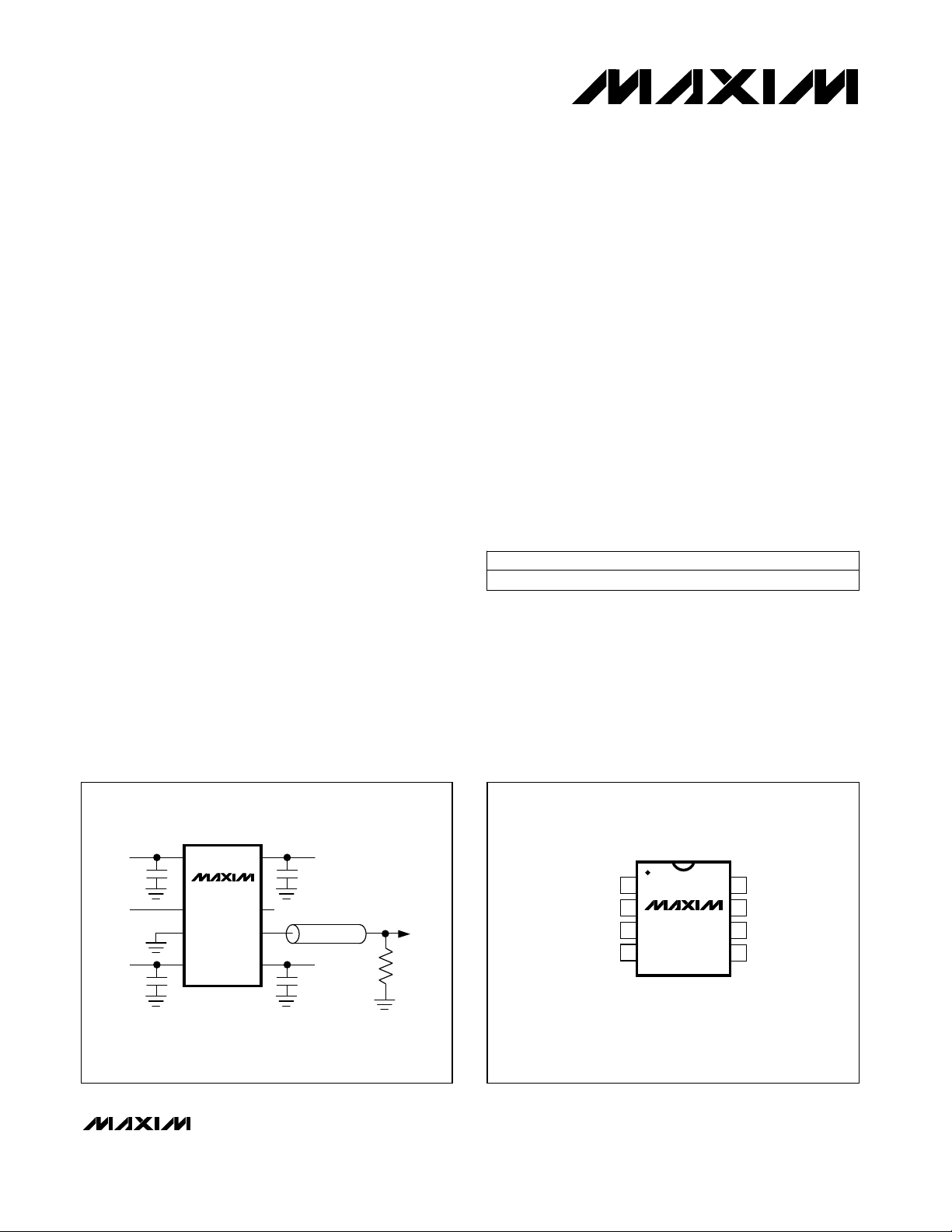
__________Typical Operating Circuit
-5V
INPUT
+5V
1
MAX4005
2
3
4
________________________________________________________________
8
7
6
5
N.C.
-5V
Z = 75Ω
+5V
R
L
OUT
= 75Ω
__________________Pin Configuration
TOP VIEW
1
V
EE
2
GND
V
IN
CC
MAX4005
3
4
Maxim Integrated Products
Call toll free 1-800-998-8800 for free samples or literature.
SO
8
V
EE
7
PEAK
6
OUT
5
V
CCO
1

950MHz FET-Input Buffer with 75ΩOutput
ABSOLUTE MAXIMUM RATINGS
Input Voltage.......................................................................±2.5V
Supply Voltage............................................................+5.5V
V
CC
Output-Stage Supply .........................................................+5.5V
Supply Voltage..............................................................-5.5V
V
EE
Peaking Pad Voltage.............................................................0.0V
Stresses beyond those listed under “Absolute Maximum Ratings” may cause permanent damage to the device. These are stress ratings only, and functional
operation of the device at these or any other conditions beyond those indicated in the operational sections of the specifications is not implied. Exposure to
absolute maximum rating conditions for extended periods may affect device reliability.
Ground Voltage.....................................................................0.0V
Continuous Power Dissipation (T
Operating Temperature Range...............................0°C to +70°C
Lead Temperature (soldering, 10sec).............................+300°C
= +70°C)...................471mW
A
MAX4005
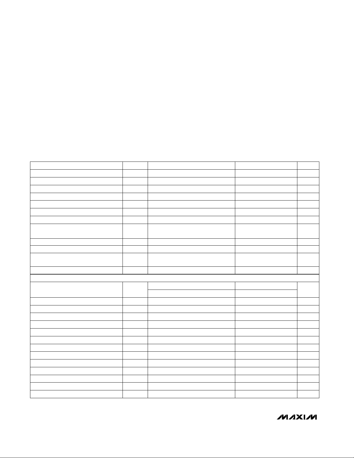
ELECTRICAL CHARACTERISTICS
(VCC= 4.75V to 5.25V, VEE= -4.75V to -5.25V, TA= +25°C, stated performance characterized for TA= 0°C to +70°C, unless
otherwise noted.)
CONDITIONS
+5V VCCCurrent
+5V Output Stage Quiescent Current
-5V VEECurrent
Output Resistance
Input Current
+5V Output Stage Power-Supply
Rejection Ratio
TYPICAL OPERATING PERFORMANCE (VCC= 5.0V, VEE= -5.0V, RL= 75Ω, TA= +25°C, unless otherwise noted.)
Input Capacitance
Settling Time to 0.1%
Rise/Fall Times
Overdrive Recovery Time
VCC1
VCC2
VEE
OUT
BWBandwidth
SET
RISE/tFALL
OD
VIN= 0V, RL= 75Ω
= 0V, RL= 75Ω
V
IN
VIN= 0V, RL= 75Ω
RL= 75Ω, gain = 0.5
VIN= 0V
B
RL= 75Ω
RL= 75Ω, measured over input
dynamic range
RL= 75Ω, gain = 0.5
VIN= 0V, RL= 75Ω
VIN= 0V, RL= 75Ω
VIN= 0V, RL= 75Ω
-3dB
-6dB 2000
IN
VIN= 0.25V step, V
VIN= 0.25V step with < 30ps rise time ps350t
At 30MHz dB±0.01GFGain Flatness
VIN= 2.5V step with 200ps rise time V/µs1000SRSlew Rate
VIN= 2.5V step ns5t
At 50MHz dBc-502HD2nd Harmonic Distortion
At 50MHz dBc< -603HD3rd Harmonic Distortion
At 100MHz dBm28TOI3rd-Order Intercept
At 3.58MHz %0.11DGDifferential Gain Error
At 3.58MHz degrees0.03DPDifferential Phase Error
OUT
= 0.125V step ns2t
0.49 0.50 0.51Gain
950
UNITSMIN TYP MAXSYMBOLPARAMETER
MHz
MHz60GF1Gain Flatness ±0.1dB
MHz80GF2Gain Flatness ±0.2dB
mA91419I
mA91114I
mA17 24 31I
mV-3 3Output Offset Voltage
Ω74.0 75.0 76.5R
nA-1 0.01 1I
%0.50 1Linearity
V-1.3 1.6Input Dynamic Range
dB40 55+5V VCCPower-Supply Rejection Ratio
dB50 75
dB40 60-5V VEEPower-Supply Rejection Ratio
pF2.2C
2 _______________________________________________________________________________________
 Loading...