

General Description
The MAX4003 low-cost, low-power logarithmic amplifier
is designed to detect the power levels of RF power
amplifiers (PAs) operating from 100MHz to 2500MHz. A
typical dynamic range of 45dB makes this logarithmic
amplifier useful in a variety of wireless applications
including cellular handset PA control, TSSI for wireless
terminal devices, and other transmitter power measurements. This logarithmic amplifier provides much wider
measurement range and superior accuracy than typical
diode-based detectors. Excellent temperature stability is
achieved over the full operating range of -40°C to +85°C.
The MAX4003 logarithmic amplifier is a voltage-measuring device with a typical signal range of -58dBV to
-13dBV. The input signal is internally AC-coupled by an
on-chip 5pF capacitor in series with a 2kΩ resistance.
This highpass coupling, with a corner at 16MHz, sets
the lowest operating frequency and allows the input
signal source to be DC grounded. The MAX4003 also
features a power-on delay, which holds the detector
output (OUT) low for approximately 5µs to ensure
glitchless controller output.
The MAX4003 is available in an 8-bump chip-scale package (UCSP™), an 8-pin µMAX package, and an 8-pin thin
QFN package. The device consumes 5.9mA with a 3.0V
supply and only 13µA when the device is in shutdown.
Applications
Cellular Handsets (TDMA, CDMA, GPRS, GSM)
TSSI for Wireless Terminal Devices
Transmitter Power Measurement and Control
RSSI for Fiber Modules
Features
♦ Complete RF Detector
♦ Frequency Range from 100MHz to 2500MHz
♦ Input Range of -58dBV to -13dBV
(-45dBm to 0dBm into 50Ω)
♦ Fast Response: 70ns in 10dB Steps
♦ Low-Current Consumption: 5.9mA at V
CC
= 3.0V
♦ 13µA (typ) Shutdown Current
♦ Available in 8-Bump UCSP or 8-Pin µMAX and
Thin QFN Packages
MAX4003
100MHz to 2500MHz, 45dB RF Detector
in a UCSP
________________________________________________________________ Maxim Integrated Products 1
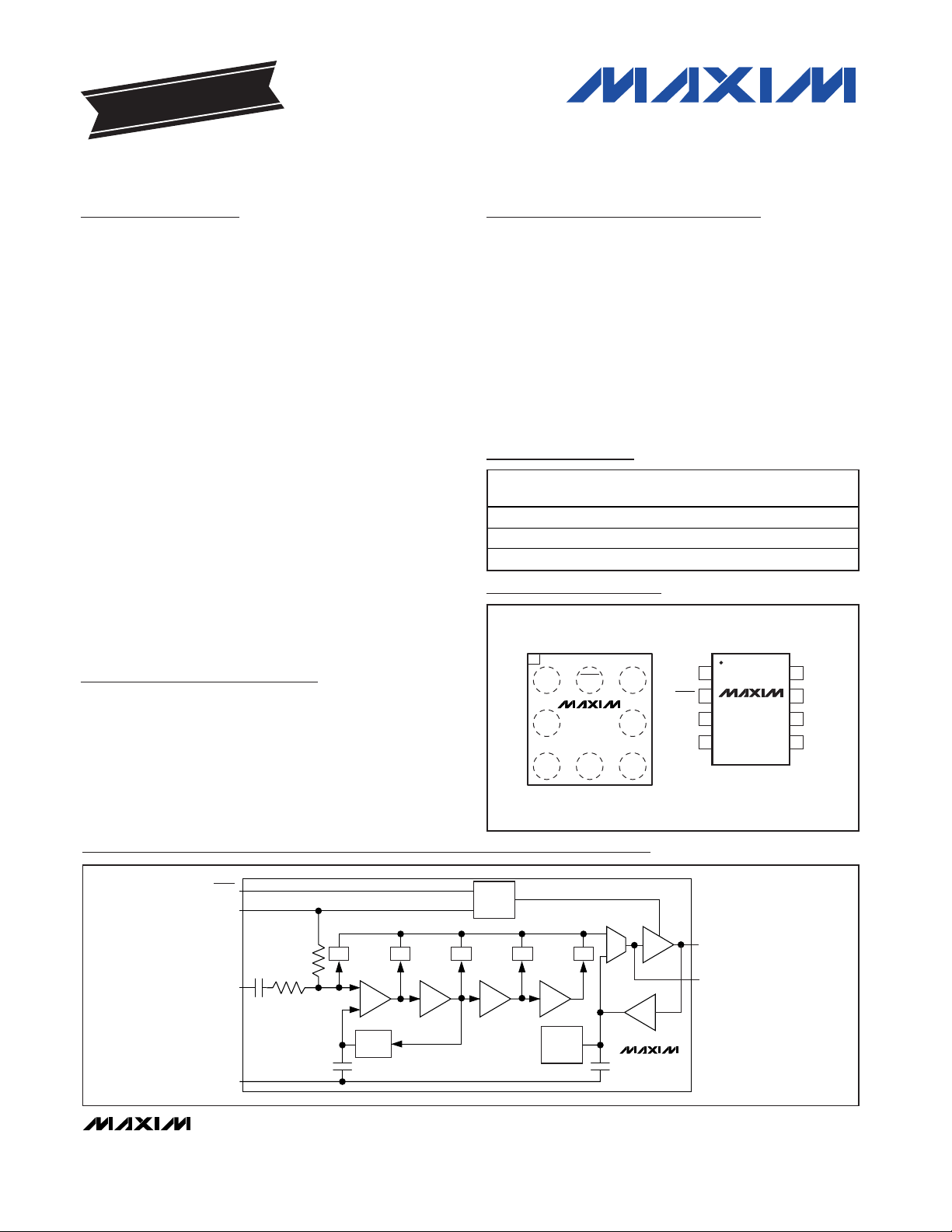
Ordering Information
10dB
DET
10dB 10dB10dB
DET
DET DETDET
OFFSET
COMP
LOW-
NOISE
BANDGAP
OUTPUT
ENABLE
DELAY
GND
g
m
+
-
1X
V-I
RFIN
V
CC
SHDN
OUT
CLPF
MAX4003
Functional Diagram
19-2620; Rev 1; 3/03
For pricing, delivery, and ordering information, please contact Maxim/Dallas Direct! at
1-888-629-4642, or visit Maxim’s website at www.maxim-ic.com.
PART
TEMP RANGE
PIN/BUMPPACKAGE
TOP
MARK
MAX4003EBL-T
8 UCSP-8 ABV
MAX4003EUA
8 µMAX —
MAX4003ETA-T
ADG
Pin Configurations
MAX4003
1
2
3
4
8
7
6
5
V
CC
OUT
N.C.
GND
CLPF
A
123
B
C
GND
RFIN
µMAX
SHDN
RFIN GND
V
CC
CLPF
V
CC
OUT GND
SHDN
MAX4003
UCSP
TOP VIEW
(BUMPS ON BOTTOM)
TOP VIEW
UCSP is a trademark of Maxim Integrated Products, Inc.
Pin Configurations continued at end of data sheet.
EVALUATION KIT
AVAILABLE
-40°C to +85°C
-40°C to +85°C
-40°C to +85°C8 Thi n QFN - E P
MAX4003
100MHz to 2500MHz, 45dB RF Detector
in a UCSP
2 _______________________________________________________________________________________
ABSOLUTE MAXIMUM RATINGS
Stresses beyond those listed under “Absolute Maximum Ratings” may cause permanent damage to the device. These are stress ratings only, and functional
operation of the device at these or any other conditions beyond those indicated in the operational sections of the specifications is not implied. Exposure to
absolute maximum rating conditions for extended periods may affect device reliability.
VCCto GND.........................................................-0.3V to +5.25V
SHDN, CLPF to GND..................................-0.3V to (VCC+ 0.3V)
RFIN..................................................................................+6dBm
OUT Short Circuit to GND.......................................................10s
Continuous Power Dissipation (T
A
= +70°C)
8-Bump UCSP (derate 4.7mW/°C above +70°C).........379mW
8-Pin µMAX (derate 4.5mW/°C above +70°C) .............362mW
8-Pin Thin QFN (derate 24.4mW/°C above +70°C) ...1951mW
Operating Temperature Range ...........................-40°C to +85°C
Junction Temperature......................................................+150°C
Storage Temperature Range .............................-65°C to +150°C
Lead Temperature (soldering, 10s) .................................+300°C
DC ELECTRICAL CHARACTERISTICS
(VCC= 3.0V, V
SHDN
= VCC, C
CLPF
= 0.1µF, TA= -40°C to +85°C. Typical values are at TA= +25°C, unless otherwise noted.) (Note 1)
PARAMETER
SYMBOL
CONDITIONS
MIN
TYP
MAX
UNITS
Supply Voltage V
CC
2.7 5.0 V
V
SHDN
= 1.8V 5.9 10 mA
Supply Current I
CC
VCC = 5.0V
V
SHDN
= 0.8V 13 30 µA
V
SHDN
= 3.0V 5 20
Shutdown Input Current I
SHDN
V
SHDN
= 0V
±5
µA
Logic High Threshold Voltage V
IH
1.8 V
Logic Low Threshold Voltage V
IL
0.8 V
DETECTOR OUTPUT
RFIN = 0dBm
Voltage Range V
OUT
RFIN = -45dBm
V
Output Voltage in Shutdown V
OUT
V
SHDN
= 0V 1 mV
Output-Referred Noise fo =150kHz 8
nV/√Hz
Small-Signal Bandwidth BW C
CLPF
= 150pF 8 MHz
Slew Rate V
OUT
= 0.36V to 1.45V, C
CLPF
= 150pF 5 V/µs
-0.01
1.45
0.36
MAX4003
100MHz to 2500MHz, 45dB RF Detector
in a UCSP
_______________________________________________________________________________________ 3
Note 1: All devices are 100% production tested at TA= +25°C and are guaranteed by design for TA= -40°C to +85°C as specified.
All production AC tests are done at 100MHz.
Note 2: Typical minimum and maximum range of the detector.
AC ELECTRICAL CHARACTERISTICS
(VCC= 3.0V, V
SHDN
= VCC, C
CLPF
= 0.1µF, fRF= 100MHz to 2500MHz, TA= -40°C to +85°C. Typical values are at TA= +25°C,
unless otherwise noted.) (Note 1)
PARAMETER
SYMBOL
CONDITIONS
MIN
TYP
MAX
UNITS
RF Input Frequency Range f
RF
MHz
RF Input Voltage Range V
RF
(Note 2) -58 -13 dBV
Equivalent RF Input Power Range
P
RF
With 50Ω termination (Note 2) -45 0
dBm
fRF = 100MHz, TA = +25°C
fRF = 100MHz
fRF = 900MHz
Logarithmic Slope
f
RF
= 1900MHz
mV/dB
fRF = 100MHz, TA = +25°C
-57
fRF = 100MHz -64 -50
fRF = 900MHz -57
Logarithmic Intercept P
X
fRF = 1900MHz -56
dBm
R
IN
2kΩ
RFIN Input Impedance
C
IN
0.5 pF
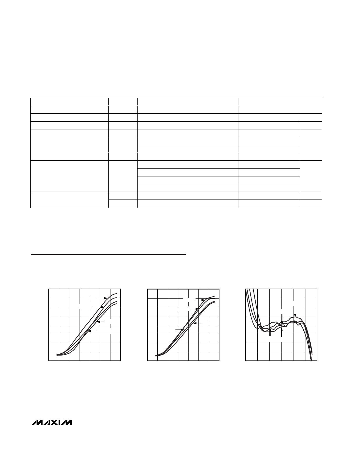
OUTPUT VOLTAGE
vs. INPUT POWER (µMAX)
MAX4003 toc01
INPUT POWER (dBm)
V
OUT
(V)
0-10-50 -40 -30 -20
0.4
0.6
0.8
1.0
1.2
1.4
1.6
1.8
0.2
-60 10
2.5GHz
1.9GHz
0.9GHz
0.1GHz
OUTPUT VOLTAGE
vs. INPUT POWER (UCSP)
MAX4003 toc02
INPUT POWER (dBm)
V
OUT
(V)
0-10-30 -20-40-50
0.2
0.4
0.6
0.8
1.0
1.2
1.4
1.6
1.8
-60 10
2.5GHz
1.9GHz
0.9GHz
0.1GHz
LOG CONFORMANCE
vs. INPUT POWER (µMAX)
MAX4003 toc03
INPUT POWER (dBm)
ERROR (dB)
0-10-40 -30 -20
-3
-2
-1
0
1
2
3
4
-4
-50 10
2.5GHz
1.9GHz
0.9GHz
0.1GHz
Typical Operating Characteristics
(VCC= V
SHDN
= 3.0V, C
CLPF
= 0.1µF, TA= +25°C, unless otherwise noted.)
100 2500
22.8 25.5 28.2
22.5 28.5
25.0
29.0
-62.3
-51.7
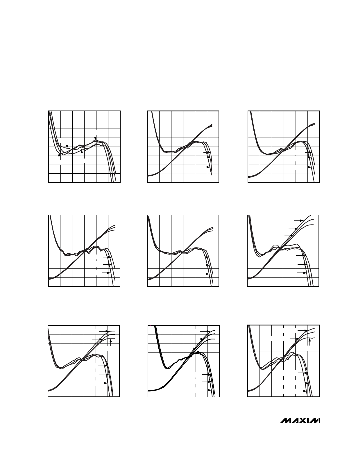
Typical Operating Characteristics (continued)
(VCC= V
SHDN
= 3.0V, C
CLPF
= 0.1µF, TA= +25°C, unless otherwise noted.)
MAX4003
100MHz to 2500MHz, 45dB RF Detector
in a UCSP
4 _______________________________________________________________________________________
LOG CONFORMANCE
vs. INPUT POWER (UCSP)
MAX4003 toc4
INPUT POWER (dBm)
ERROR (dB)
0-10-40 -30 -20
-3
-2
-1
0
1
2
3
4
-4
-50 10
2.5GHz
0.9GHz
0.1GHz
1.9GHz
V
OUT
AND LOG CONFORMANCE
vs. INPUT POWER AT 0.1GHz (µMAX)
MAX4003 toc05
INPUT POWER (dBm)
V
OUT
(V)
0-10-40 -30 -20
0.4
0.6
0.8
1.0
1.2
1.4
1.6
1.8
0.2
-3
-2
-1
0
1
2
3
4
-4
-50 10
TA = +85°C
TA = +25°C
TA = -40°C
ERROR (dB)
V
OUT
AND LOG CONFORMANCE
vs. INPUT POWER AT 0.1GHz (UCSP)
MAX4003 toc06
INPUT POWER (dBm)
V
OUT
(V)
0-10-40 -30 -20
0.4
0.6
0.8
1.0
1.2
1.4
1.6
1.8
0.2
-3
-2
-1
0
1
2
3
4
-4
-50 10
TA = +85°C
TA = +25°C
TA = -40°C
ERROR (dB)
V
OUT
AND LOG CONFORMANCE
vs. INPUT POWER AT 0.9GHz (µMAX)
MAX4003 toc07
INPUT POWER (dBm)
V
OUT
(V)
ERROR (dB)
0-10-40 -30 -20
0.4
0.6
0.8
1.0
1.2
1.4
1.6
1.8
0.2
-3
-2
-1
0
1
2
3
4
-4
-50 10
TA = +85°C
TA = +25°C
TA = -40°C
V
OUT
AND LOG CONFORMANCE
vs. INPUT POWER AT 0.9GHz (UCSP)
MAX4003 toc08
INPUT POWER (dBm)
V
OUT
(V)
0-10-40 -30 -20
0.4
0.6
0.8
1.0
1.2
1.4
1.6
1.8
0.2
-3
-2
-1
0
1
2
3
4
-4
-50 10
TA = +85°C
TA = +25°C
TA = -40°C
ERROR (dB)
V
OUT
AND LOG CONFORMANCE
vs. INPUT POWER AT 1.9GHz (µMAX)
MAX4003 toc09
INPUT POWER (dBm)
V
OUT
(V)
ERROR (dB)
0-10-40 -30 -20
0.4
0.6
0.8
1.0
1.2
1.4
1.6
1.8
0.2
-3
-2
-1
0
1
2
3
4
-4
-50 10
TA = +85°C
TA = +25°C
TA = -40°C
TA = +85°C
TA = +25°C
TA = -40°C
V
OUT
AND LOG CONFORMANCE
vs. INPUT POWER AT 1.9GHz (UCSP)
MAX4003 toc10
INPUT POWER (dBm)
V
OUT
(V)
ERROR (dB)
0-10-40 -30 -20
0.4
0.6
0.8
1.0
1.2
1.4
1.6
1.8
0.2
-3
-2
-1
0
1
2
3
4
-4
-50 10
TA = +85°C
TA = +25°C
TA = -40°C
TA = +85°C
TA = +25°C
TA = -40°C
V
OUT
AND LOG CONFORMANCE
vs. INPUT POWER AT 2.5GHz (µMAX)
MAX4003 toc11
INPUT POWER (dBm)
V
OUT
(V)
ERROR (dB)
0-10-40 -30 -20
0.4
0.6
0.8
1.0
1.2
1.4
1.6
1.8
0.2
-3
-2
-1
0
1
2
3
4
-4
-50 10
TA = +85°C
TA = +25°C
TA = -40°C
TA = +85°C
TA = +25°C
TA = -40°C
V
OUT
AND LOG CONFORMANCE
vs. INPUT POWER AT 2.5GHz (UCSP)
MAX4003 toc12
INPUT POWER (dBm)
V
OUT
(V)
ERROR (dB)
0-10-40 -30 -20
0.4
0.6
0.8
1.0
1.2
1.4
1.6
1.8
0.2
-3
-2
-1
0
1
2
3
4
-4
-50 10
TA = +85°C
TA = +25°C
TA = -40°C
TA = +85°C
TA = +25°C
TA = -40°C

Typical Operating Characteristics (continued)
(VCC= V
SHDN
= 3.0V, C
CLPF
= 0.1µF, TA= +25°C, unless otherwise noted.)
MAX4003
100MHz to 2500MHz, 45dB RF Detector
in a UCSP
_______________________________________________________________________________________ 5
LOG SLOPE vs. FREQUENCY (µMAX)
MAX4003 toc13
FREQUENCY (GHz)
LOG SLOPE (mV/dB)
2.01.51.00.5
25
26
27
28
29
30
31
24
0 2.5
TA = +25°C
TA = -40°C
TA = +85°C
LOG SLOPE vs. FREQUENCY (UCSP)
MAX4003 toc14
FREQUENCY (GHz)
LOG SLOPE (mV/dB)
2.01.51.00.5
25
26
27
28
29
30
31
24
0 2.5
TA = +25°C
TA = +85°C
TA = -40°C
LOG SLOPE vs. SUPPLY VOLTAGE (µMAX)
MAX4003 toc15
VCC (V)
LOG SLOPE (mV/dB)
5.04.53.0 3.5 4.0
25
26
27
28
29
30
31
32
24
2.5 5.5
2.5GHz
1.9GHz
0.9GHz
0.1GHz
LOG SLOPE (mV/dB)
LOG SLOPE vs. SUPPLY VOLTAGE (UCSP)
5.04.54.03.53.02.5 5.5
MAX4003 toc16
25
26
27
28
29
30
31
32
24
V
CC
(V)
0.9GHz
2.5GHz
1.9GHz
0.1GHz
LOG INTERCEPT vs. FREQUENCY (µMAX)
MAX4003 toc17
FREQUENCY (GHz)
LOG INTERCEPT (dBm)
2.01.51.00.5
-58
-57
-56
-55
-54
-53
-52
-51
-50
-59
0 2.5
TA = +25°C
TA = -40°C
TA = +85°C
LOG INTERCEPT (dBm)
-60
-59
-58
-57
-56
-55
-61
LOG INTERCEPT vs. FREQUENCY (UCSP)
2.01.51.00.50 2.5
MAX4003 toc18
FREQUENCY (GHz)
TA = +85°C
TA = +25°C
TA = -40°C
LOG INTERCEPT
vs. SUPPLY VOLTAGE
(µMAX)
MAX4003 toc19
VCC (V)
LOG INTERCEPT (dBm)
5.04.54.03.53.0
-59
-58
-57
-56
-55
-54
-53
-52
-51
-50
-49
-60
2.5 5.5
2.5GHz
1.9GHz
0.9GHz
0.1GHz
5.04.54.03.53.02.5 5.5
MAX4003 toc20
-60
-59
-58
-57
-56
-55
-61
V
CC
(V)
LOG INTERCEPT (dBm)
LOG INTERCEPT
vs. SUPPLY VOLTAGE (UCSP)
1.9GHz
2.5GHz
0.1GHz
0.9GHz
RFIN INPUT IMPEDANCE
vs. FREQUENCY (µMAX)
MAX4003 toc21
FREQUENCY (GHz)
RESISTANCE (Ω)
REACTANCE (Ω)
2.01.51.00.5
500
1000
1500
R
X
2000
2500
0
-400
-300
-200
-100
0
-500
-600
-700
-800
0 2.5
FREQUENCY (GHz) R JX
Ω
0.1 2100 -794
0.9 500 -91
1.9 52 -35
2.5 27 -366

MAX4003
100MHz to 2500MHz, 45dB RF Detector
in a UCSP
6 _______________________________________________________________________________________
OUTPUT NOISE SPECTRAL DENSITY
MAX4003 toc26
FREQUENCY (Hz)
NOISE SPECTRAL DENSITY (nV/√Hz)
1k 10k 100k 1M
10
1
100 10M
9
8
7
6
5
4
3
2
MAXIMUM OUTPUT VOLTAGE
vs. SUPPLY VOLTAGE
MAX40003 toc27
VCC (V)
V
OUT
(V)
5.04.53.0 3.5 4.0
1.54
1.56
1.58
1.60
1.62
1.64
1.66
1.68
1.52
2.5 5.5
fRF = 900MHz, P
RFIN
= +5dBm
I
LOAD
= 0mA, 5mA, 10mA
RFIN INPUT IMPEDANCE
vs. FREQUENCY (UCSP)
MAX4003 toc22
FREQUENCY (GHz)
RESISTANCE (Ω)
REACTANCE (Ω)
2.01.51.00.5
500
1000
1500
R
X
2000
2500
0
-400
-300
-200
-100
0
-500
-600
-700
-800
02.5
FREQUENCY (GHz) R JX
Ω
0.1 1916 -839
0.9 909 -125
1.9 228 -48
2.5 102 -29
SUPPLY CURRENT
vs. SHUTDOWN VOLTAGE
MAX4003 toc23
V
SHDN
(V)
SUPPLY CURRENT (mA)
1.81.61.41.21.00.80.60.40.2
0
1
2
3
4
5
6
7
-1
0 2.0
POWER-ON RESPONSE TIME
MAX4003 toc24
2µs/div
V
OUT
500mV/div
1.5V/div
V
SHDN
5µs
POWER-DOWN RESPONSE TIME
MAX4003 toc25
2µs/div
V
OUT
500mV/div
1.5V/div
V
SHDN
Typical Operating Characteristics (continued)
(VCC= V
SHDN
= 3.0V, C
CLPF
= 0.1µF, TA= +25°C, unless otherwise noted.)

MAX4003
100MHz to 2500MHz, 45dB RF Detector
in a UCSP
_______________________________________________________________________________________ 7
MINIMUM OUTPUT VOLTAGE
vs. SUPPLY VOLTAGE
MAX4003 toc28
VCC (V)
V
OUT
(V)
5.04.54.03.53.0
0.33
0.34
0.35
0.36
0.37
0.38
0.39
0.40
0.41
0.32
2.5 5.5
fRF = 900MHz, P
RFIN
= -50dBm
I
LOAD
= 0mA, 5mA, 10mA
SMALL-SIGNAL STEP RESPONSE
(C
CLPF
= 150pF)
MAX4003 toc29
1µs/div
550
500
450
400
V
OUT
(mV)
350
300
250
fRF = 900MHz
100mV
P-P
SMALL-SIGNAL STEP RESPONSE
(C
CLPF
= 1000pF)
MAX4003 toc30
1µs/div
550
500
450
400
V
OUT
(mV)
350
300
250
fRF = 900MHz
100mV
P-P
LARGE-SIGNAL STEP RESPONSE
(C
CLPF
= 150pF)
MAX4003 toc31
1µs/div
1600
1400
1200
1000
V
OUT
(mV)
800
600
400
fRF = 900MHz
1V
P-P
LARGE-SIGNAL STEP RESPONSE
(C
CLPF
= 1000pF)
MAX4003 toc32
1µs/div
1600
1400
1200
1000
V
OUT
(mV)
800
600
400
fRF = 900MHz
1V
P-P
10
0.1
100 10,000 100,000
1
C
CLPF
(pF)
FREQUENCY (MHz)
1000
SMALL-SIGNAL BANDWIDTH
vs. C
CLPF
MAX4003 toc33
Typical Operating Characteristics (continued)
(VCC= V
SHDN
= 3.0V, C
CLPF
= 0.1µF, TA= +25°C, unless otherwise noted.)

MAX4003
100MHz to 2500MHz, 45dB RF Detector
in a UCSP
8 _______________________________________________________________________________________
Detailed Description
The MAX4003 logarithmic amplifier comprises four
main amplifier/limiter stages, each with a small-signal
gain of 10dB. The output stage of each amplifier/limiter
stage is applied to a full-wave rectifier (detector). A
detector stage also precedes the first stage. In total,
five detectors, each separated by 10dB, comprise the
logarithmic amplifier strip (see Functional Diagram).
A portion of the PA output power is coupled into RFIN
of the logarithmic amplifier detector through a directional coupler, and is applied to the logarithmic amplifier
strip. Each detector stage generates a rectified current,
and these currents are summed to form a logarithmic
function. The detected output is applied to a high-gain
transconductance (gm) stage, which is buffered and
then applied to OUT. OUT is applied to an ADC typically found in the baseband IC which, in turn, controls the
PA biasing with its DAC output (Figure 1).
In a control loop, the detector output voltage range is
approximately 0.36V for the minimum input signal,
-45dBm, to 1.45V at the maximum input range, 0dBm.
The logarithmic intercept of the detector output with
respect to the RF input can be obtained by drawing a
best fit line of the Output Voltage vs. RF Input Power
graph. The logarithmic slope is defined as the change
in the detector output vs. the change in RF input. The
MAX4003 slope at low frequencies is approximately
25.5mV/dB. Variation in temperature and supply voltage does not alter the slope significantly, as shown in
the Typical Operating Characteristics.
Applications Information
Filter Capacitor and Transient Response
In general, the choice of filter only partially determines
the time-domain response of a PA detector loop.
However, some simple conventions may be applied to
discuss transient response. A large filter capacitor,
C
CLPF
, dominates time-domain response, but the loop
bandwidth remains a factor of the PA gain-control range
(see Typical Operating Characteristics). The bandwidth
is maximized at power outputs near the center of the
PA’s range and minimized at the low and high power levels, when the slope of the gain control curve is lowest.
A smaller valued C
CLPF
results in an increased-loop
bandwidth inversely proportional to the capacitor value.
Inherent phase lag in the PA’s control path, usually
caused by parasitics at the OUT pin, ultimately results
in the addition of complex poles in the AC loop equation. To avoid this secondary effect, experimentally
determine the lowest usable C
CLPF
for the power ampli-
V
CC
OUT
N.C.
GNDCLPF
GND
RFIN
MAX4003
SHDN
V
CC
XX
PA
50Ω
50Ω
C
CLPF
0.01µF
TRANSMITTER
DAC
ADC
BASEBAND
IC
Figure 1. MAX4003 Typical Application Circuit
Pin Description
PIN
µMAX/
Thin QFN
NAME
DESCRIPTION
1A1RFIN RF Input. Requires off-chip 50Ω impedance match.
2A2
Shutdown Input. A logic LOW on SHDN shuts down the entire IC.
3, 5
GND Ground. Connect to PC board ground plane.
4B3CLPF
Lowpass Filter Connection. Connect external capacitor between CLPF and GND to set the
control-loop bandwidth.
6—N.C. No Connection. Leave this pin unconnected or connect to GND.
7C2OUT Detector Output. Connect this buffer output to baseband ADC.
8
V
CC
Supply Voltage. Bypass with capacitor as close to the pin as possible. The bypass capacitor
must not share its ground vias with any other branches.
UCSP
SHDN
A3, C3
B1, C1

MAX4003
100MHz to 2500MHz, 45dB RF Detector
in a UCSP
_______________________________________________________________________________________ 9
fier of interest. This requires full consideration of the
intricacies of the PA detector control function. The
worst-case condition, where the PA output is smallest
(gain function is steepest), should be used because the
PA control function is nonlinear. An additional zero can
be added to improve loop dynamics by placing a resistor in series with C
CLPF
.
Waveform Considerations
Although the input level of the MAX4003 is specified in
dBm, the logarithmic amplifier actually responds to rectified voltage signals rather than a true RMS power. It is
important to realize that input signals with identical rootmean-square power but with unique waveforms result
in different logarithmic outputs.
Differing signal waveforms result in either an upward or
downward shift in the logarithmic intercept. However,
the logarithmic slope remains the same.
Layout Considerations
As with any RF circuit, the MAX4003 circuit layout
affects performance. To ensure maximum power transfer between 50Ω sources and the MAX4003 input, suitable matching networks should be implemented. The
VCCinput should be bypassed as close as possible to
the device with multiple vias connecting the capacitor
to the ground plane.
UCSP Reliability
The UCSP represents a unique package that greatly
reduces board space compared to other packages.
UCSP reliability is integrally linked to the user’s assembly methods, circuit board material, and usage environment. The user should closely review these areas when
considering use of a UCSP. This form factor may not
perform equally to a packaged product through traditional mechanical reliability tests. Performance through
operating life test and moisture resistance remains
uncompromised as it is primarily determined by the
wafer fabrication process. Mechanical stress performance is a greater consideration for a UCSP. UCSP
solder joint contact integrity must be considered since
the package is attached through direct solder contact
to the user’s PC board. Testing done to characterize
the UCSP reliability performance shows that it can perform reliably through environmental stresses. Results of
environmental stress tests and additional usage data
and recommendations are detailed in the UCSP
application note found on Maxim’s website,
www.maxim-ic.com.
Chip Information
TRANSISTOR COUNT: 358
Pin Configurations (continued)
THIN QFN
TOP VIEW
MAX4003
N.C.
GND
87V
CC
OUT
6
5
CLPF
1
2SHDN
GND
RFIN
3
4

MAX4003
100MHz to 2500MHz, 45dB RF Detector
in a UCSP
10 ______________________________________________________________________________________
Package Information
(The package drawing(s) in this data sheet may not reflect the most current specifications. For the latest package outline information,
go to www.maxim-ic.com/packages
.)
8LUMAXD.EPS
PACKAGE OUTLINE, 8L uMAX/uSOP
1
1
21-0036
J
REV.DOCUMENT CONTROL NO.APPROVAL
PROPRIETARY INFORMATION
TITLE:
MAX
0.043
0.006
0.014
0.120
0.120
0.198
0.026
0.007
0.037
0.0207 BSC
0.0256 BSC
A2
A1
c
e
b
A
L
FRONT VIEW
SIDE VIEW
E H
0.6±0.1
0.6±0.1
Ø0.50±0.1
1
TOP VIEW
D
8
A2
0.030
BOTTOM VIEW
1
6°
S
b
L
H
E
D
e
c
0°
0.010
0.116
0.116
0.188
0.016
0.005
8
4X S
INCHES
-
A1
A
MIN
0.002
0.950.75
0.5250 BSC
0.25 0.36
2.95 3.05
2.95 3.05
4.78
0.41
0.65 BSC
5.03
0.66
6°0°
0.13 0.18
MAX
MIN
MILLIMETERS
- 1.10
0.05 0.15
α
α
DIM

MAX4003
100MHz to 2500MHz, 45dB RF Detector
in a UCSP
______________________________________________________________________________________ 11
Package Information (continued)
(The package drawing(s) in this data sheet may not reflect the most current specifications. For the latest package outline information,
go to www.maxim-ic.com/packages
.)
6, 8, &10L, DFN THIN.EPS
COMMON DIMENSIONS
SYMBOL MIN. MAX.
A 0.70 0.80
D 2.90 3.10
E 2.90 3.10
A1
0.00 0.05
L 0.20 0.40
PKG. CODE N D2 E2 e JEDEC SPEC b
[(N/2)-1] x e
PACKAGE VARIATIONS
0.25 MIN.k
A2 0.20 REF.
2.00 REF0.25±0.050.50 BSC2.30±0.1010T1033-1
2.40 REF0.20±0.05- - - - 0.40 BSC1.70±0.10 2.30±0.1014T1433-1
1.50±0.10 MO229 / WEED-3
0.40 BSC - - - - 0.20±0.05 2.40 REFT1433-2 14 2.30±0.101.70±0.10
T633-2 6 1.50±0.10 2.30±0.10 0.95 BSC MO229 / WEEA 0.40±0.05 1.90 REF
T833-2 8 1.50±0.10 2.30±0.10 0.65 BSC MO229 / WEEC 0.30±0.05 1.95 REF
T833-3 8 1.50±0.10 2.30±0.10 0.65 BSC MO229 / WEEC 0.30±0.05 1.95 REF
2.30±0.10 MO229 / WEED-3 2.00 REF0.25±0.050.50 BSC1.50±0.1010T1033-2

MAX4003
100MHz to 2500MHz, 45dB RF Detector
in a UCSP
Maxim cannot assume responsibility for use of any circuitry other than circuitry entirely embodied in a Maxim product. No circuit patent licenses are
implied. Maxim reserves the right to change the circuitry and specifications without notice at any time.
12 ____________________Maxim Integrated Products, 120 San Gabriel Drive, Sunnyvale, CA 94086 408-737-7600
© 2003 Maxim Integrated Products Printed USA is a registered trademark of Maxim Integrated Products.
Package Information (continued)
(The package drawing(s) in this data sheet may not reflect the most current specifications. For the latest package outline information,
go to www.maxim-ic.com/packages
.)
9LUCSP, 3x3.EPS
PACKAGE OUTLINE, 3x3 UCSP
21-0093
1
1
K
 Loading...