

19-2288; Rev 2; 12/07
2.5GHz 45dB RF-Detecting Controllers
General Description
The MAX4000/MAX4001/MAX4002 low-cost, low-power
logarithmic amplifiers are designed to control RF power
amplifiers (PA) operating in the 0.1GHz to 2.5GHz frequency range. A typical dynamic range of 45dB makes
this family of log amps useful in a variety of wireless applications including cellular handset PA control, transmitter
power measurement, and RSSI for terminal devices.
Logarithmic amplifiers provide much wider measurement
range and superior accuracy to controllers based on
diode detectors. Excellent temperature stability is
achieved over the full operating range of -40°C to +85°C.
The choice of three different input voltage ranges eliminates the need for external attenuators, thus simplifying
PA control-loop design. The logarithmic amplifier is a voltage-measuring device with a typical signal range of
-58dBV to -13dBV for the MAX4000, -48dBV to -3dBV for
the MAX4001, and -43dBV to +2dBV for the MAX4002.
The input signal for the MAX4000 is internally AC-coupled
using an on-chip 5pF capacitor in series with a 2kΩ input
resistance. This highpass coupling, with a corner at
16MHz, sets the lowest operating frequency and allows
the input signal source to be DC grounded. The
MAX4001/MAX4002 require an external coupling capacitor in series with the RF input port. These PA controllers
feature a power-on delay when coming out of shutdown,
holding OUT low for approximately 5µs to ensure glitchfree controller output.
The MAX4000/MAX4001/MAX4002 family is available in
an 8-pin µMAX
package (UCSP™). The device consumes 5.9mA with a
5.5V supply, and when powered down the typical shutdown current is 13µA.
®
package and an 8-bump chip-scale
Features
♦ Complete RF-Detecting PA Controllers
♦ Variety of Input Ranges
MAX4000: -58dBV to -13dBV
(-45dBm to 0dBm in 50Ω)
MAX4001: -48dBV to -3dBV
(-35dBm to +10dBm in 50Ω)
MAX4002: -43dBV to +2dBV
(-30dBm to +15dBm in 50Ω)
♦ Frequency Range from 100MHz to 2.5GHz
♦ Temperature Stable Linear-in-dB Response
♦ Fast Response: 70ns 10dB Step
♦ 10mA Output Sourcing Capability
♦ Low Power: 17mW at 3V (typ)
♦ Shutdown Current 30µA (max)
♦ Available in an 8-Bump UCSP and a Small 8-Pin
µMAX Package
Ordering Information
PART TEMP RANGE
MAX4000EBL-T -40°C to +85°C 8 UCSP-8
MAX4000EUA -40°C to +85°C 8 µMAX
MAX4001EBL-T -40°C to +85°C 8 UCSP-8
MAX4001EUA -40°C to +85°C 8 µMAX
MAX4002EBL-T -40°C to +85°C 8 UCSP-8
MAX4002EUA -40°C to +85°C 8 µMAX
PINPACKAGE
TOP
MARK
ABF
—
ABE
—
ABD
—
MAX4000/MAX4001/MAX4002
Applications
Pin Configurations appear at end of data sheet.
Transmitter Power Measurement and Control
TSSI for Wireless Terminal Devices
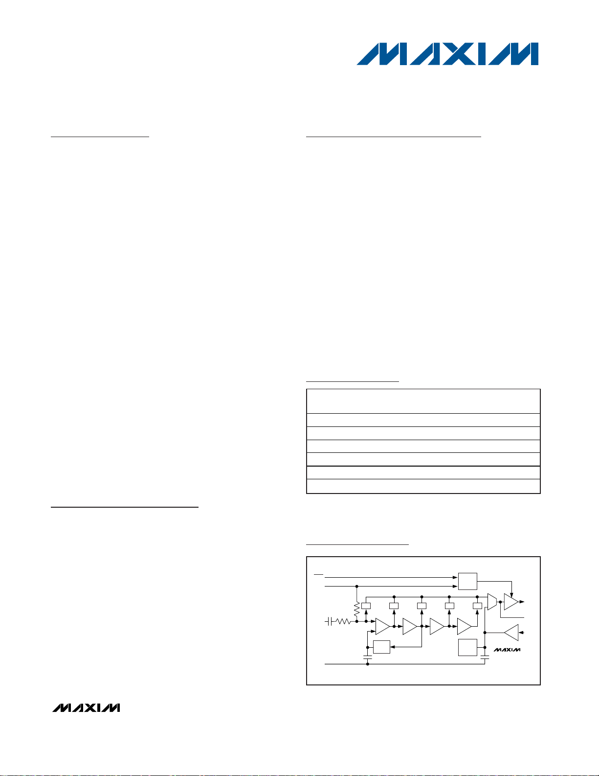
Functional Diagram
Cellular Handsets (TDMA, CDMA, GPRS, GSM)
RSSI for Fiber Modules
OUTPUT
ENABLE
DELAY
gm
X1
MAX4000
OUT
CLPF
SET
V-I
DET DETDET
LOWNOISE
BANDGAP
+
µMAX is a registered trademark of Maxim Integrated Products, Inc.
UCSP is a trademark of Maxim Integrated Products, Inc.
________________________________________________________________ Maxim Integrated Products 1
SHDN
V
CC
RFIN
GND
(PADDLE)
OFFSET
COMP
DET
DET
10dB
10dB 10dB10dB
For pricing, delivery, and ordering information, please contact Maxim Direct at 1-888-629-4642,
or visit Maxim’s website at www.maxim-ic.com.

MAX4000/MAX4001/MAX4002
2.5GHz 45dB RF-Detecting Controllers
2 _______________________________________________________________________________________
ABSOLUTE MAXIMUM RATINGS
Stresses beyond those listed under “Absolute Maximum Ratings” may cause permanent damage to the device. These are stress ratings only, and functional
operation of the device at these or any other conditions beyond those indicated in the operational sections of the specifications is not implied. Exposure to
absolute maximum rating conditions for extended periods may affect device reliability.
ELECTRICAL CHARACTERISTICS
(VCC= 3V, SHDN = 1.8V, TA= -40°C to +85°C, unless otherwise noted. Typical values are at TA= +25°C.) (Note 1)
PARAMETER
CONDITIONS MIN
UNITS
Supply Voltage V
CC
2.7 5.5 V
Supply Current I
CC
VCC = 5.5V 5.9 9.3 mA
Shutdown Supply Current I
CC
SHDN = 0.8V, VCC = 5.5V 13 30 µA
Shutdown Output Voltage V
OUT
SHDN = 0.8V 100 mV
Logic-High Threshold V
H
1.8 V
Logic-Low Threshold V
L
0.8 V
SHDN = 3V 5 20
SHDN Input Current I
SHDN
SHDN = 0 -0.8
µA
SET-POINT INPUT
Voltage Range (Note 2) V
SET
Corresponding to central 40dB
1.45 V
Input Resistance R
IN
30 MΩ
Slew Rate (Note 3) 16 V/µs
MAIN OUTPUT
High, I
SOURCE
= 10mA
Voltage Range V
OUT
Low, I
SINK
= 350µA
V
Output-Referred Noise From CLPF 8
nV/√Hz
Small-Signal Bandwidth BW From CLPF 20 MHz
Slew Rate
V/µs
(Voltages Referenced to GND)
V
CC
...........................................................................-0.3V to +6V
OUT, SET, SHDN, CLPF.............................-0.3V to (V
CC
+ 0.3V)
RFIN
MAX4000 ......................................................................+6dBm
MAX4001 ....................................................................+16dBm
MAX4002 ....................................................................+19dBm
Equivalent Voltage
MAX4000 ..................................................................0.45V
RMS
MAX4001 ....................................................................1.4V
RMS
MAX4002 ....................................................................2.0V
RMS
OUT Short Circuit to GND ..........................................Continuous
Continuous Power Dissipation (TA = +70°C)
8-Bump UCSP (derate 4.7mW/°C above +70°C).........379mW
8-Pin µMAX (derate 4.5mW/°C above +70°C) .............362mW
Operating Temperature Range ...........................-40°C to +85°C
Storage Temperature Range .............................-65°C to +150°C
Lead Temperature (soldering , 10s) ................................+300°C
SYMBOL
TYP MAX
-0.01
0.35
V
= 0.2V to 2.6V 8
OUT
2.65 2.75
0.15
MAX4000/MAX4001/MAX4002
2.5GHz 45dB RF-Detecting Controllers
_______________________________________________________________________________________ 3
Note 1: All devices are 100% production tested at TA= +25°C and are guaranteed by design for TA= -40°C to +85°C as specified.
All production AC testing is done at 100MHz.
Note 2: Typical value only, set-point input voltage range determined by logarithmic slope and logarithmic intercept.
Note 3: Set-point slew rate is the rate at which the reference level voltage, applied to the inverting input of the g
m
stage, responds to
a voltage step at the SET pin (see Figure 1).
Note 4: Typical min/max range for detector.
Note 5: MAX4000 internally AC-coupled.
Note 6: MAX4001/MAX4002 are internally resistive-coupled to V
CC
.
ELECTRICAL CHARACTERISTICS
(VCC= 3V, SHDN = 1.8V, fRF= 100MHz to 2.5GHz, TA= -40°C to +85°C, unless otherwise noted. Typical values are at TA= +25°C.)
(Note 1)
PARAMETER
CONDITIONS MIN TYP
UNITS
RF Input Frequency f
RF
100
MHz
MAX4000 -58 -13
MAX4001 -48 -3
RF Input Voltage Range
(Note 4)
V
RF
MAX4002 -43 +2
dBV
MAX4000 -45 0
MAX4001 -35 +10
Equivalent Power Range
(50Ω Terminated) (Note 4)
P
RF
MAX4002 -30 +15
dBm
f
RF
= 100MHz 22.5 25.5 28.5
f
RF
= 900MHz 25Logarithmic Slope V
S
f
RF
= 1900MHz 29
mV/dB
MAX4000 -62 -55 -49
MAX4001 -52 -45 -39fRF = 100MHz
MAX4002 -47 -40 -34
MAX4000 -57
MAX4001 -48
fRF = 900MHz
MAX4002 -43
MAX4000 -56
MAX4001 -45
Logarithmic Intercept P
X
fRF = 1900MHz
MAX4002 -41
dBm
RF INPUT INTERFACE
DC Resistance R
DC
MAX4001/MAX4002, connected to V
CC
(Note 5)
2kΩ
Inband Resistance R
IB
2kΩ
Inband Capacitance C
IB
MAX4000, internally AC-coupled
(Note 6)
0.5 pF
SYMBOL
MAX
2500
MAX4000/MAX4001/MAX4002
2.5GHz 45dB RF-Detecting Controllers
4 _______________________________________________________________________________________
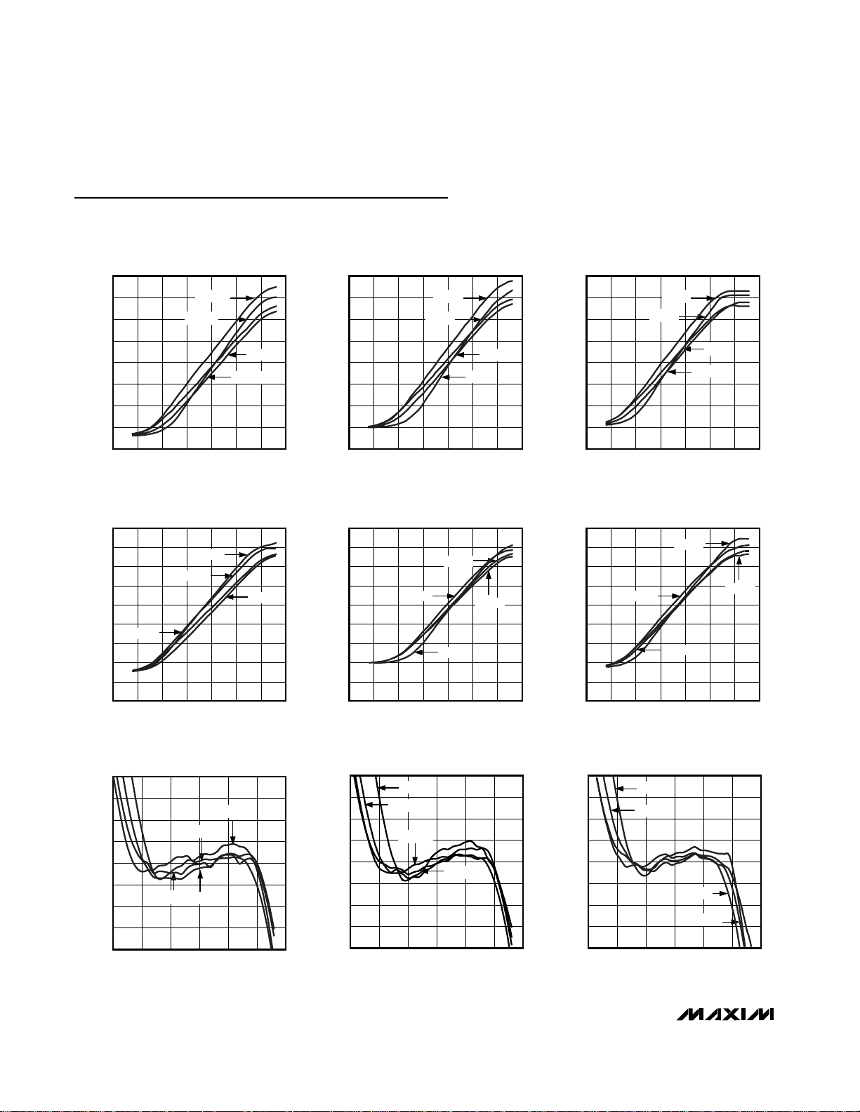
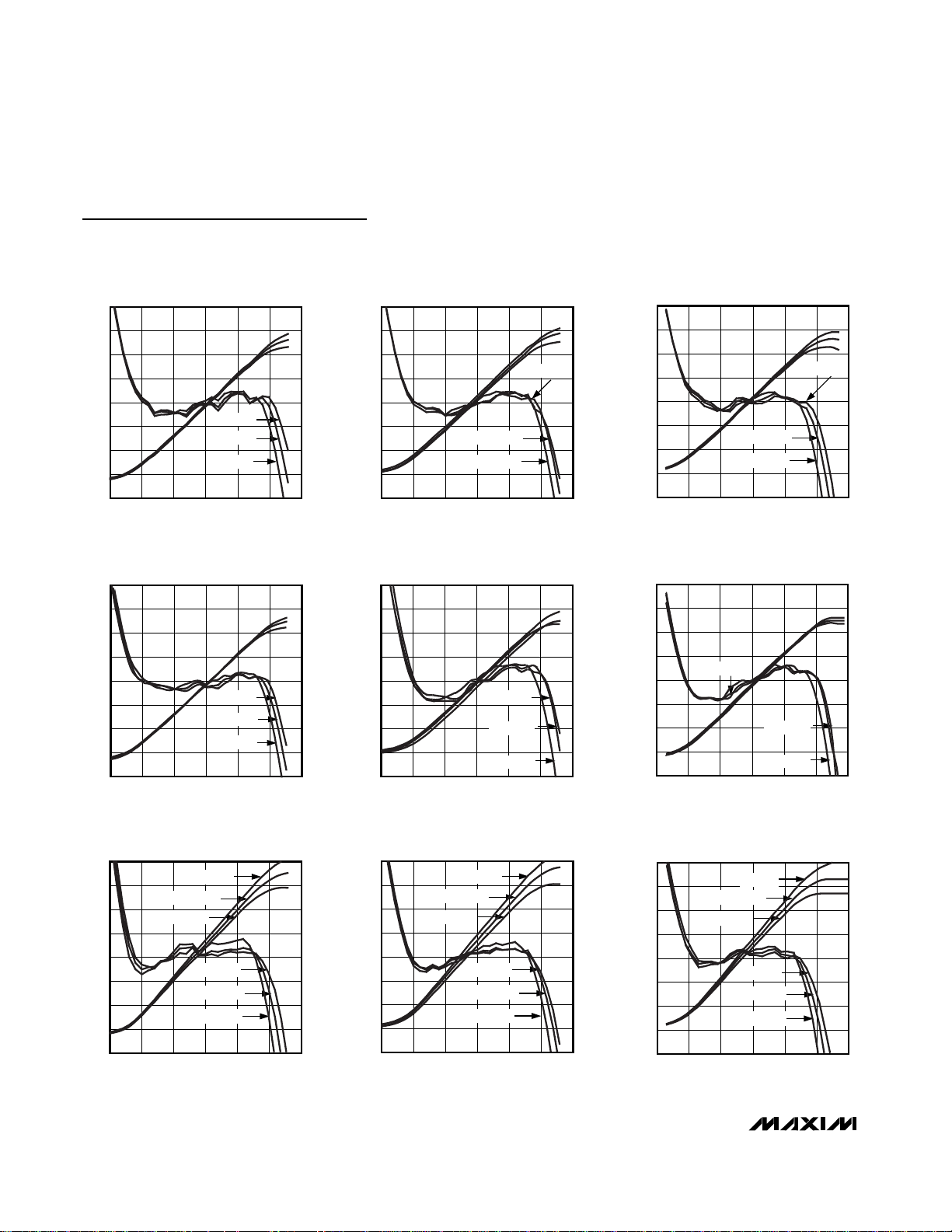
Typical Operating Characteristics
(VCC= 3V, SHDN = VCC, TA= +25°C, unless otherwise specified. All log conformance plots are normalized to their respective temperatures.)
MAX4001 LOG CONFORMANCE
vs. INPUT POWER (μMAX)
MAX4000 toc08
INPUT POWER (dBm)
ERROR (dB)
100-30 -20 -10
-3
-2
-1
0
1
2
3
4
-4
-40 20
2.5GHz
1.9GHz
0.9GHz
0.1GHz
MAX4002 LOG CONFORMANCE
vs. INPUT POWER (μMAX)
MAX4000 toc09
INPUT POWER (dBm)
ERROR (dB)
155-25 -15 -5
-3
-2
-1
0
1
2
3
4
-4
-35 25
2.5GHz
1.9GHz
0.9GHz
0.1GHz
MAX4000 LOG CONFORMANCE
vs. INPUT POWER (μMAX)
MAX4000 toc07
INPUT POWER (dBm)
ERROR (dB)
0-10-40 -30 -20
-3
-2
-1
0
1
2
3
4
-4
-50 10
2.5GHz
1.9GHz
0.9GHz
0.1GHz
MAX4002
SET vs. INPUT POWER (UCSP)
MAX4000 toc06
INPUT POWER (dBm)
SET (V)
2010-10 0-20-30
0.2
0.4
0.6
0.8
1.0
1.2
1.4
1.6
1.8
0
-40 30
2.5GHz
1.9GHz
0.9GHz
0.1GHz
MAX4001
SET vs. INPUT POWER (UCSP)
INPUT POWER (dBm)
SET (V)
100-20 -10-30-40
0.2
0.4
0.6
0.8
1.0
1.2
1.4
1.6
1.8
0
-50 20
2.5GHz
1.9GHz
0.9GHz
0.1GHz
MAX4000 toc05
MAX4000
SET vs. INPUT POWER (UCSP)
MAX4000 toc04
INPUT POWER (dBm)
SET (V)
0-10-30 -20-40-50
0.2
0.4
0.6
0.8
1.0
1.2
1.4
1.6
1.8
0
-60 10
2.5GHz
1.9GHz
0.9GHz
0.1GHz
MAX4002
SET vs. INPUT POWER (μMAX)
MAX4000 toc03
INPUT POWER (dBm)
SET (V)
2010-30 -20 -10 0
0.4
0.6
0.8
1.0
1.2
1.4
1.6
1.8
0.2
-40 30
2.5GHz
1.9GHz
0.9GHz
0.1GHz
MAX4001
SET vs. INPUT POWER (μMAX)
MAX4000 toc02
INPUT POWER (dBm)
SET (V)
100-40 -30 -20 -10
0.4
0.6
0.8
1.0
1.2
1.4
1.6
1.8
0.2
-50 20
2.5GHz
1.9GHz
0.9GHz
0.1GHz
MAX4000
SET vs. INPUT POWER (μMAX)
MAX4000 toc01
INPUT POWER (dBm)
SET (V)
0-10-50 -40 -30 -20
0.4
0.6
0.8
1.0
1.2
1.4
1.6
1.8
0.2
-60 10
2.5GHz
1.9GHz
0.9GHz
0.1GHz
MAX4000/MAX4001/MAX4002
2.5GHz 45dB RF-Detecting Controllers
_______________________________________________________________________________________ 5
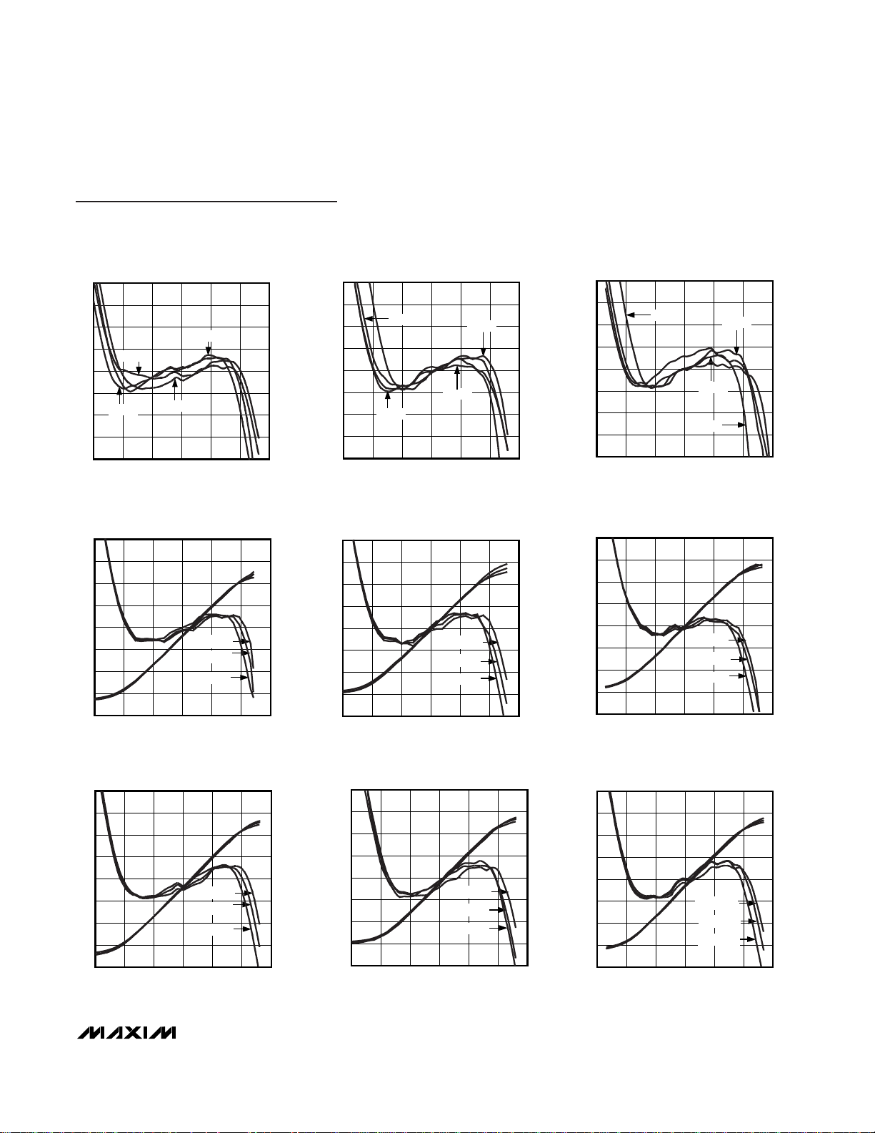
Typical Operating Characteristics (continued)
(VCC= 3V, SHDN = VCC, TA= +25°C, unless otherwise specified. All log conformance plots are normalized to their respective temperatures.)
MAX4002 SET AND LOG CONFORMANCE
vs. INPUT POWER AT 0.1GHz (UCSP)
MAX4000 toc18
INPUT POWER (dBm)
SET (V)
155-25 -15 -5
0.4
0.6
0.8
1.0
1.2
1.4
1.6
1.8
0.2
-3
-2
-1
0
1
2
3
4
-4
-35 25
TA = +85°C
TA = +25°C
TA = -40°C
ERROR (dB)
MAX4001 SET AND LOG CONFORMANCE
vs. INPUT POWER AT 0.1GHz (UCSP)
MAX4000 toc17
INPUT POWER (dBm)
SET (V)
100-30 -20 -10
0.4
0.6
0.8
1.0
1.2
1.4
1.6
1.8
0.2
-3
-2
-1
0
1
2
3
4
-4
-40 20
TA = +85°C
TA = +25°C
TA = -40°C
ERROR (dB)
MAX4000 SET AND LOG CONFORMANCE
vs. INPUT POWER AT 0.1GHz (UCSP)
MAX4000 toc16
INPUT POWER (dBm)
SET (V)
0-10-40 -30 -20
0.4
0.6
0.8
1.0
1.2
1.4
1.6
1.8
0.2
-3
-2
-1
0
1
2
3
4
-4
-50 10
TA = +85°C
TA = +25°C
TA = -40°C
ERROR (dB)
MAX4002 SET AND LOG CONFORMANCE
vs. INPUT POWER AT 0.1GHz (μMAX)
MAX4000 toc15
INPUT POWER (dBm)
SET (V)
ERROR (dB)
155-25 -15 -5
0.4
0.6
0.8
1.0
1.2
1.4
1.6
1.8
0.2
-3
-2
-1
0
1
2
3
4
-4
-35 25
TA = +85°C
TA = +25°C
TA = -40°C
MAX4001 SET AND LOG CONFORMANCE
vs. INPUT POWER AT 0.1GHz (μMAX)
MAX4000 toc14
INPUT POWER (dBm)
SET (V)
100-30 -20 -10
0.4
0.6
0.8
1.0
1.2
1.4
1.6
1.8
0.2
-3
-2
-1
0
1
2
3
4
-4
-40 20
TA = +85°C
TA = +25°C
TA = -40°C
ERROR (dB)
MAX4000 SET AND LOG CONFORMANCE
vs. INPUT POWER AT 0.1GHz (μMAX)
MAX4000 toc13
INPUT POWER (dBm)
SET (V)
0-10-40 -30 -20
0.4
0.6
0.8
1.0
1.2
1.4
1.6
1.8
0.2
-3
-2
-1
0
1
2
3
4
-4
-50 10
TA = +85°C
TA = +25°C
TA = -40°C
ERROR (dB)
MAX4002 LOG CONFORMANCE
vs. INPUT POWER (UCSP)
MAX4000 toc12
INPUT POWER (dBm)
ERROR (dB)
155-25 -15 -5
-3
-2
-1
0
1
2
3
4
-4
-35 25
2.5GHz
0.9GHz
0.1GHz
1.9GHz
MAX4001 LOG CONFORMANCE
vs. INPUT POWER (UCSP)
MAX4000 toc11
INPUT POWER (dBm)
ERROR (dB)
100-30 -20 -10
-3
-2
-1
0
1
2
3
4
-4
-40 20
2.5GHz
0.9GHz
0.1GHz
1.9GHz
MAX4000 LOG CONFORMANCE
vs. INPUT POWER (UCSP)
MAX4000 toc10
INPUT POWER (dBm)
ERROR (dB)
0-10-40 -30 -20
-3
-2
-1
0
1
2
3
4
-4
-50 10
2.5GHz
0.9GHz
0.1GHz
1.9GHz
MAX4000/MAX4001/MAX4002
2.5GHz 45dB RF-Detecting Controllers
6 _______________________________________________________________________________________
Typical Operating Characteristics (continued)
(VCC= 3V, SHDN = VCC, TA= +25°C, unless otherwise specified. All log conformance plots are normalized to their respective temperatures.)
MAX4002 SET AND LOG CONFORMANCE
vs. INPUT POWER AT 1.9GHz (μMAX)
MAX4000 toc27
INPUT POWER (dBm)
SET (V)
ERROR (dB)
155-25 -15 -5
0.4
0.6
0.8
1.0
1.2
1.4
1.6
1.8
0.2
-3
-2
-1
0
1
2
3
4
-4
-35 25
TA = +85°C
TA = +25°C
TA = -40°C
TA = +85°C
TA = +25°C
TA = -40°C
MAX4001 SET AND LOG CONFORMANCE
vs. INPUT POWER AT 1.9GHz (μMAX)
MAX4000 toc26
INPUT POWER (dBm)
SET (V)
ERROR (dB)
100-30 -20 -10
0.4
0.6
0.8
1.0
1.2
1.4
1.6
1.8
0.2
-3
-2
-1
0
1
2
3
4
-4
-40 20
TA = +85°C
TA = +25°C
TA = -40°C
TA = +85°C
TA = +25°C
TA = -40°C
MAX4000 SET AND LOG CONFORMANCE
vs. INPUT POWER AT 1.9GHz (μMAX)
MAX4000 toc25
INPUT POWER (dBm)
SET (V)
ERROR (dB)
0-10-40 -30 -20
0.4
0.6
0.8
1.0
1.2
1.4
1.6
1.8
0.2
-3
-2
-1
0
1
2
3
4
-4
-50 10
TA = +85°C
TA = +25°C
TA = -40°C
TA = +85°C
TA = +25°C
TA = -40°C
MAX4002 SET AND LOG CONFORMANCE
vs. INPUT POWER AT 0.9GHz (UCSP)
MAX4000 toc24
INPUT POWER (dBm)
SET (V)
155-25 -15 -5
0.4
0.6
0.8
1.0
1.2
1.4
1.6
1.8
0.2
-3
-2
-1
0
1
2
3
4
-4
-35 25
TA = +85°C
TA = +25°C
TA = -40°C
ERROR (dB)
MAX4001 SET AND LOG CONFORMANCE
vs. INPUT POWER AT 0.9GHz (UCSP)
MAX4000 toc23
INPUT POWER (dBm)
SET (V)
100-30 -20 -10
0.4
0.6
0.8
1.0
1.2
1.4
1.6
1.8
0.2
-3
-2
-1
0
1
2
3
4
-4
-40 20
TA = +85°C
TA = +25°C
TA = -40°C
ERROR (dB)
MAX4000 SET AND LOG CONFORMANCE
vs. INPUT POWER AT 0.9GHz (UCSP)
MAX4000 toc22
INPUT POWER (dBm)
SET (V)
0-10-40 -30 -20
0.4
0.6
0.8
1.0
1.2
1.4
1.6
1.8
0.2
-3
-2
-1
0
1
2
3
4
-4
-50 10
TA = +85°C
TA = +25°C
TA = -40°C
ERROR (dB)
MAX4002 SET AND LOG CONFORMANCE
vs. INPUT POWER AT 0.9GHz (μMAX)
MAX4000 toc21
INPUT POWER (dBm)
SET (V)
ERROR (dB)
155-25 -15 -5
0.4
0.6
0.8
1.0
1.2
1.4
1.6
1.8
0.2
-3
-2
-1
0
1
2
3
4
-4
-35 25
TA = +85°C
TA = +25°C
TA = -40°C
MAX4001 SET AND LOG CONFORMANCE
vs. INPUT POWER AT 0.9GHz (μMAX)
MAX4000 toc20
INPUT POWER (dBm)
SET (V)
ERROR (dB)
100-30 -20 -10
0.4
0.6
0.8
1.0
1.2
1.4
1.6
1.8
0.2
-3
-2
-1
0
1
2
3
4
-4
-40 20
TA = +85°C
TA = +25°C
TA = -40°C
MAX4000 SET AND LOG CONFORMANCE
vs. INPUT POWER AT 0.9GHz (μMAX)
MAX4000 toc19
INPUT POWER (dBm)
SET (V)
ERROR (dB)
0-10-40 -30 -20
0.4
0.6
0.8
1.0
1.2
1.4
1.6
1.8
0.2
-3
-2
-1
0
1
2
3
4
-4
-50 10
TA = +85°C
TA = +25°C
TA = -40°C

MAX4000/MAX4001/MAX4002
2.5GHz 45dB RF-Detecting Controllers
_______________________________________________________________________________________ 7
Typical Operating Characteristics (continued)
(VCC= 3V, SHDN = VCC, TA= +25°C, unless otherwise specified. All log conformance plots are normalized to their respective temperatures.)
MAX4001 SET AND LOG CONFORMANCE
vs. INPUT POWER AT 2.5GHz (UCSP)
MAX4000 toc35
INPUT POWER (dBm)
SET (V)
ERROR (dB)
100-30 -20 -10
0.4
0.6
0.8
1.0
1.2
1.4
1.6
1.8
0.2
-3
-2
-1
0
1
2
3
4
-4
-40 20
TA = +85°C
TA = +25°C
TA = -40°C
TA = +85°C
TA = +25°C
TA = -40°C
MAX4000 SET AND LOG CONFORMANCE
vs. INPUT POWER AT 2.5GHz (UCSP)
MAX4000 toc34
INPUT POWER (dBm)
SET (V)
ERROR (dB)
0-10-40 -30 -20
0.4
0.6
0.8
1.0
1.2
1.4
1.6
1.8
0.2
-3
-2
-1
0
1
2
3
4
-4
-50 10
TA = +85°C
TA = +25°C
TA = -40°C
TA = +85°C
TA = +25°C
TA = -40°C
MAX4002 SET AND LOG CONFORMANCE
vs. INPUT POWER AT 2.5GHz (μMAX)
MAX4000 toc33
INPUT POWER (dBm)
SET (V)
ERROR (dB)
155-25 -15 -5
0.4
0.6
0.8
1.0
1.2
1.4
1.6
1.8
0.2
-3
-2
-1
0
1
2
3
4
-4
-35 25
TA = +85°C
TA = +25°C
TA = -40°C
TA = +85°C
TA = +25°C
TA = -40°C
MAX4001 SET AND LOG CONFORMANCE
vs. INPUT POWER AT 2.5GHz (μMAX)
MAX4000 toc32
INPUT POWER (dBm)
SET (V)
ERROR (dB)
100-30 -20 -10
0.4
0.6
0.8
1.0
1.2
1.4
1.6
1.8
0.2
-3
-2
-1
0
1
2
3
4
-4
-40 20
TA = +85°C
TA = +25°C
TA = -40°C
TA = +85°C
TA = +25°C
TA = -40°C
MAX4000 SET AND LOG CONFORMANCE
vs. INPUT POWER AT 2.5GHz (μMAX)
MAX4000 toc31
INPUT POWER (dBm)
SET (V)
ERROR (dB)
0-10-40 -30 -20
0.4
0.6
0.8
1.0
1.2
1.4
1.6
1.8
0.2
-3
-2
-1
0
1
2
3
4
-4
-50 10
TA = +85°C
TA = +25°C
TA = -40°C
TA = +85°C
TA = +25°C
TA = -40°C
MAX4002 SET AND LOG CONFORMANCE
vs. INPUT POWER AT 1.9GHz (UCSP)
MAX4000 toc30
INPUT POWER (dBm)
SET (V)
ERROR (dB)
155-25 -15 -5
0.4
0.6
0.8
1.0
1.2
1.4
1.6
1.8
0.2
-3
-2
-1
0
1
2
3
4
-4
-35 25
TA = -40°C
TA = +85°C
TA = +25°C
TA = -40°C
MAX4001 SET AND LOG CONFORMANCE
vs. INPUT POWER AT 1.9GHz (UCSP)
MAX4000 toc29
INPUT POWER (dBm)
SET (V)
ERROR (dB)
100-30 -20 -10
0.4
0.6
0.8
1.0
1.2
1.4
1.6
1.8
0.2
-3
-2
-1
0
1
2
3
4
-4
-40 20
TA = +85°C
TA = +25°C
TA = -40°C
TA = +85°C
TA = +25°C
TA = -40°C
MAX4000 SET AND LOG CONFORMANCE
vs. INPUT POWER AT 1.9GHz (UCSP)
MAX4000 toc28
INPUT POWER (dBm)
SET (V)
ERROR (dB)
0-10-40 -30 -20
0.4
0.6
0.8
1.0
1.2
1.4
1.6
1.8
0.2
-3
-2
-1
0
1
2
3
4
-4
-50 10
TA = +85°C
TA = +25°C
TA = -40°C
TA = +85°C
TA = +25°C
TA = -40°C
MAX4002 SET AND LOG CONFORMANCE
vs. INPUT POWER AT 2.5GHz (UCSP)
MAX4000 toc36
INPUT POWER (dBm)
SET (V)
ERROR (dB)
155-25 -15 -5
0.4
0.6
0.8
1.0
1.2
1.4
1.6
1.8
0.2
-3
-2
-1
0
1
2
3
4
-4
-35 25
TA = +85°C
TA = -40°C
TA = +25°C

MAX4000/MAX4001/MAX4002
2.5GHz 45dB RF-Detecting Controllers
8 _______________________________________________________________________________________
Typical Operating Characteristics (continued)
(VCC= 3V, SHDN = VCC, TA= +25°C, unless otherwise specified. All log conformance plots are normalized to their respective temperatures.)
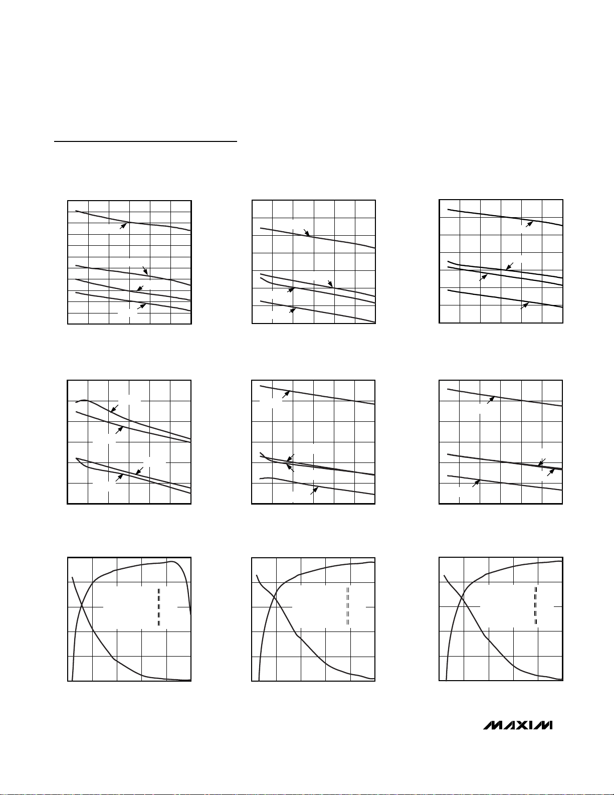
MAX4002
LOG SLOPE vs. V
CC
(μMAX)
MAX4000 toc45
VCC (V)
LOG SLOPE (mV/dB)
5.04.54.03.53.0
25
26
27
28
29
30
31
32
33
34
24
2.5 5.5
1.9GHz
0.9GHz
0.1GHz
2.5GHz
MAX4001
LOG SLOPE vs. V
CC
(μMAX)
MAX4000 toc44
VCC (V)
LOG SLOPE (mV/dB)
5.04.53.0 3.5 4.0
25
26
27
28
29
30
31
32
24
2.5 5.5
2.5GHz
1.9GHz
0.9GHz
0.1GHz
MAX4000
LOG SLOPE vs. V
CC
(μMAX)
MAX4000 toc43
VCC (V)
LOG SLOPE (mV/dB)
5.04.53.0 3.5 4.0
25
26
27
28
29
30
31
32
24
2.5 5.5
2.5GHz
1.9GHz
0.9GHz
0.1GHz
FREQUENCY (GHz)
LOG SLOPE (mV/dB)
25
26
27
28
29
30
31
32
24
MAX4002
LOG SLOPE vs. FREQUENCY (UCSP)
2.01.51.00.50 2.5
MAX4000 toc42
TA = +25°C
TA = +85°C
TA = -40°C
MAX4001
LOG SLOPE vs. FREQUENCY (UCSP)
FREQUENCY (GHz)
LOG SLOPE (mV/dB)
25
26
27
28
29
30
31
32
23
24
MAX4000 toc41
2.01.51.00.50 2.5
TA = +25°C
TA = +85°C
TA = -40°C
MAX4000
LOG SLOPE vs. FREQUENCY (UCSP)
MAX4000 toc40
FREQUENCY (GHz)
LOG SLOPE (mV/dB)
2.01.51.00.5
25
26
27
28
29
30
31
24
0 2.5
TA = +25°C
TA = +85°C
TA = -40°C
MAX4002
LOG SLOPE vs. FREQUENCY (μMAX)
MAX4000 toc39
FREQUENCY (GHz)
LOG SLOPE (mV/dB)
2.01.51.00.5
25
26
27
28
29
30
31
32
33
24
0 2.5
TA = +25°C
TA = -40°C
TA = +85°C
MAX4001
LOG SLOPE vs. FREQUENCY (μMAX)
MAX4000 toc38
FREQUENCY (GHz)
LOG SLOPE (mV/dB)
2.01.51.00.5
24
25
26
27
28
29
30
31
32
23
0 2.5
TA = +25°C
TA = -40°C
TA = +85°C
MAX4000
LOG SLOPE vs. FREQUENCY (μMAX)
MAX4000 toc37
FREQUENCY (GHz)
LOG SLOPE (mV/dB)
2.01.51.00.5
25
26
27
28
29
30
31
24
0 2.5
TA = +25°C
TA = -40°C
TA = +85°C

MAX4000/MAX4001/MAX4002
2.5GHz 45dB RF-Detecting Controllers
_______________________________________________________________________________________ 9
Typical Operating Characteristics (continued)
(VCC= 3V, SHDN = VCC, TA= +25°C, unless otherwise specified. All log conformance plots are normalized to their respective temperatures.)
2.01.51.00.50 2.5
-44
-42
-40
-38
-36
-34
-32
-46
MAX4000 toc54
LOG INTERCEPT (dB)
MAX4002
LOG INTERCEPT vs. FREQUENCY (UCSP)
FREQUENCY (GHz)
TA = +85°C
TA = +25°C
TA = -40°C
-50
-48
-46
-44
-42
-40
-52
2.01.51.00.50 2.5
MAX4000 toc53
FREQUENCY (GHz)
LOG INTERCEPT (dBm)
MAX4001
LOG INTERCEPT vs. FREQUENCY (UCSP)
TA = +85°C
TA = +25°C
TA = -40°C
LOG INTERCEPT (dBm)
-60
-59
-58
-57
-56
-55
-61
MAX4000
LOG INTERCEPT vs. FREQUENCY (UCSP)
2.01.51.00.50 2.5
MAX4000 toc52
FREQUENCY (GHz)
TA = +85°C
TA = +25°C
TA = -40°C
MAX4002
LOG INTERCEPT vs. FREQUENCY (μMAX)
MAX4000 toc51
FREQUENCY (GHz)
LOG INTERCEPT (dBm)
2.01.51.00.5
-44
-42
-40
-38
-36
-34
-32
-46
0 2.5
TA = +25°C
TA = -40°C
TA = +85°C
MAX4001
LOG INTERCEPT vs. FREQUENCY (μMAX)
MAX4000 toc50
FREQUENCY (GHz)
LOG INTERCEPT (dBm)
2.01.51.00.5
-48
-47
-46
-45
-44
-43
-42
-41
-40
-39
-49
0 2.5
TA = +25°C
TA = -40°C
TA = +85°C
MAX4000
LOG INTERCEPT vs. FREQUENCY (μMAX)
MAX4000 toc49
FREQUENCY (GHz)
LOG INTERCEPT (dBm)
2.01.51.00.5
-58
-57
-56
-55
-54
-53
-52
-51
-50
-59
0 2.5
TA = +25°C
TA = -40°C
TA = +85°C
LOG SLOPE (mV/dB)
5.04.54.03.53.02.5 5.5
MAX4000 toc48
25
27
29
31
33
23
MAX4002
LOG SLOPE vs. V
CC
(UCSP)
VCC (V)
0.9GHz
2.5GHz
1.9GHz
0.1GHz
LOG SLOPE (mV/dB)
25
27
29
31
33
23
5.04.54.03.53.02.5 5.5
MAX4000 toc47
MAX4001
LOG SLOPE vs. V
CC
(UCSP)
VCC (V)
0.9GHz
2.5GHz
1.9GHz
0.1GHz
LOG SLOPE (mV/dB)
MAX4000
LOG SLOPE vs. V
CC
(UCSP)
5.04.54.03.53.02.5 5.5
MAX4000 toc46
25
26
27
28
29
30
31
32
24
V
CC
(V)
0.9GHz
2.5GHz
1.9GHz
0.1GHz
MAX4000/MAX4001/MAX4002
2.5GHz 45dB RF-Detecting Controllers
10 ______________________________________________________________________________________
Typical Operating Characteristics (continued)
(VCC= 3V, SHDN = VCC, TA= +25°C, unless otherwise specified. All log conformance plots are normalized to their respective temperatures.)
MAX4002 INPUT IMPEDANCE
vs. FREQUENCY (μMAX)
MAX4000 toc63
FREQUENCY (GHz)
RESISTANCE (Ω)
REACTANCE (Ω)
2.01.51.00.5
500
1000
1500
R
X
2000
2500
0
-400
-300
-200
-100
0
-500
-600
-700
-800
0 2.5
FREQUENCY (GHz) R JXΩ
0.1 2309 -1137
0.9 943 -120
1.9 129 -36
2.5 30 -26
MAX4001 INPUT IMPEDANCE
vs. FREQUENCY (μMAX)
MAX4000 toc62
FREQUENCY (GHz)
RESISTANCE (Ω)
REACTANCE (Ω)
2.01.51.00.5
500
1000
1500
R
X
2000
2500
0
-400
-300
-200
-100
0
-500
-600
-700
-800
0 2.5
FREQUENCY (GHz) R JXΩ
0.1 2144 -1205
0.9 959 -121
1.9 104 -36
2.5 47 -29
MAX4000 INPUT IMPEDANCE
vs. FREQUENCY (μMAX)
MAX4000 toc61
FREQUENCY (GHz)
RESISTANCE (Ω)
REACTANCE (Ω)
2.01.51.00.5
500
1000
1500
R
X
2000
2500
0
-400
-300
-200
-100
0
-500
-600
-700
-800
0 2.5
FREQUENCY (GHz) R JXΩ
0.1 2100 -794
0.9 500 -91
1.9 52 -35
2.5 27 -366
5.04.54.03.53.0
-44
-42
-40
-38
-36
-34
-46
2.5 5.5
MAX4000 toc60
VCC (V)
LOG INTERCEPT (dBm)
MAX4002
LOG INTERCEPT vs. V
CC
(UCSP)
1.9GHz
2.5GHz
0.1GHz
0.9GHz
5.04.54.03.53.02.5 5.5
MAX4000 toc59
-50
-48
-46
-44
-42
-40
-52
V
CC
(V)
LOG INTERCEPT (dBm)
MAX4001
LOG INTERCEPT vs. V
CC
(UCSP)
1.9GHz
2.5GHz
0.1GHz
0.9GHz
5.04.54.03.53.02.5 5.5
MAX4000 toc58
-60
-59
-58
-57
-56
-55
-61
V
CC
(V)
LOG INTERCEPT (dBm)
MAX4000
LOG INTERCEPT vs. V
CC
(UCSP)
1.9GHz
2.5GHz
0.1GHz
0.9GHz
MAX4002
LOG INTERCEPT vs. V
CC
(μMAX)
MAX4000 toc58
VCC (V)
LOG INTERCEPT (dBm)
5.04.54.03.53.0
-45
-43
-41
-39
-37
-35
-33
-47
2.5 5.5
2.5GHz
1.9GHz
0.9GHz
0.1GHz
MAX4001
LOG INTERCEPT vs. V
CC
(μMAX)
MAX4000 toc56
VCC (V)
LOG INTERCEPT (dBm)
5.04.54.03.53.0
-48
-46
-44
-42
-40
-38
-36
-50
2.5 5.5
2.5GHz
1.9GHz
0.9GHz
0.1GHz
MAX4000
LOG INTERCEPT vs. V
CC
(μMAX)
MAX4000 toc55
VCC (V)
LOG INTERCEPT (dBm)
5.04.54.03.53.0
-59
-58
-57
-56
-55
-54
-53
-52
-51
-50
-49
-60
2.5 5.5
2.5GHz
1.9GHz
0.9GHz
0.1GHz

MAX4000/MAX4001/MAX4002
2.5GHz 45dB RF-Detecting Controllers
______________________________________________________________________________________ 11
Typical Operating Characteristics (continued)
(VCC= 3V, SHDN = VCC, TA= +25°C, unless otherwise specified. All log conformance plots are normalized to their respective temperatures.)
SUPPLY CURRENT
vs. SHDN VOLTAGE
MAX4000 toc67
SHDN (V)
SUPPLY CURRENT (mA)
1.81.60.2 0.4 0.6 1.0 1.20.8 1.4
0
1
2
3
4
5
6
7
-1
0 2.0
1.2V
V
CC
= 5.5V
SHDN POWER-ON DELAY RESPONSE TIME
MAX4000 toc68
2μs/div
OUT 500mV/div
1.5V/div
SHDN
5μs
SHDN RESPONSE TIME
MAX4000 toc69
2μs/div
OUT 500mV/div
1.5V/div
SHDN
MAX4002 INPUT IMPEDANCE
vs. FREQUENCY (UCSP)
MAX4000 toc66
FREQUENCY (GHz)
RESISTANCE (Ω)
REACTANCE (Ω)
2.01.51.00.5
500
1000
1500
R
X
2000
2500
0
0 2.5
FREQUENCY (GHz) R JXΩ
0.1 1961 -1137
0.9 1130 -120
1.9 315 -36
2.5 163 -26
-400
-300
-200
-100
0
-500
-600
-700
-800
-900
-1000
MAX4000 INPUT IMPEDANCE
vs. FREQUENCY (UCSP)
MAX4000 toc64
FREQUENCY (GHz)
RESISTANCE (Ω)
REACTANCE (Ω)
2.01.51.00.5
500
1000
1500
R
X
2000
2500
0
-400
-300
-200
-100
0
-500
-600
-700
-800
0 2.5
FREQUENCY (GHz) R JXΩ
0.1 1916 -839
0.9 909 -125
1.9 228 -48
2.5 102 -29
MAX4001 INPUT IMPEDANCE
vs. FREQUENCY (UCSP)
MAX4000 toc65
FREQUENCY (GHz)
RESISTANCE (Ω)
REACTANCE (Ω)
2.01.51.00.5
500
1000
1500
R
X
2000
2500
0
-400
-300
-200
-100
0
-500
-600
-700
-800
-900
-1000
0 2.5
FREQUENCY (GHz) R JXΩ
0.1 1942 -927
0.9 1009 -136
1.9 314 -57
2.5 139 -37

MAX4000/MAX4001/MAX4002
2.5GHz 45dB RF-Detecting Controllers
12 ______________________________________________________________________________________
Pin Description
PIN
NAME
FUNCTION
1 A1 RFIN RF Input
2A2
Shutdown. Connect to VCC for normal operation.
3 A3 SET Set-Point Input for Controller Mode Operation
4 B3 CLPF
Lowpass Filter Connection. Connect external capacitor between CLPF and GND to set
control-loop bandwidth.
5 C3 GND Ground
6 — N.C. No Connection. Not internally connected.
7 C2 OUT Output to PA Gain-Control Pin
8
V
CC
Supply Voltage. VCC = 2.7V to 5.5V.
Typical Operating Characteristics (continued)
(VCC= 3V, SHDN = VCC, TA= +25°C, unless otherwise specified. All log conformance plots are normalized to their respective temperatures.)
Block Diagram
BUFFER
GND
OUTPUT-
ENABLE
DELAY
LOG
DETECTOR
x1
V-I*
SHDN
V
CC
RFIN
SET
C
CLPF
OUT
MAX4000
MAX4001
MAX4002
g
m
BLOCK
MAIN OUTPUT NOISE SPECTRAL DENSITY
10
9
8
7
6
5
4
3
2
NOISE SPECTRAL DENSITY (nV/√HZ)
MAX4000 toc70
5.5
5.0
4.5
4.0
3.5
OUT VOLTAGE (V)
3.0
2.5
MAXIMUM OUT VOLTAGE
BY LOAD CURRENT
vs. V
CC
0
5mA
10mA
MAX4000 toc71
1
1k 10k 100k 1M
100 10M
FREQUENCY (Hz)
µMAX UCSP
SHDN
B1, C1
2.0
2.5 5.5
VCC (V)
5.04.54.03.53.0

MAX4000/MAX4001/MAX4002
2.5GHz 45dB RF-Detecting Controllers
______________________________________________________________________________________ 13
Detailed Description
The MAX4000/MAX4001/MAX4002 family of logarithmic
amplifiers (log amps) is comprised of four main amplifier/limiter stages each with a small-signal gain of 10dB.
The output stage of each amplifier is applied to a fullwave rectifier (detector). A detector stage also precedes the first gain stage. In total, five detectors each
separated by 10dB, comprise the log amp strip. Figure
1 shows the functional diagram of the log amps.
A portion of the PA output power is coupled to RFIN of
the log amp controller, and is applied to the log amp
strip. Each detector cell outputs a rectified current and
all cell currents are summed and form a logarithmic
output. The detected output is applied to a high-gain
g
m
stage, which is buffered and then applied to OUT.
OUT is applied to the gain-control pin of the PA to close
the control loop. The voltage applied to SET determines
the output power of the PA in the control loop. The voltage applied to SET relates to an input power level
determined by the log amp detector characteristics.
Extrapolating a straight-line fit of the graph of SET vs.
RFIN provides the logarithmic intercept. Logarithmic
slope, the amount SET changes for each dB change of
RF input, is generally independent of waveform or termination impedance. The MAX4000/MAX4001/
MAX4002 slope at low frequencies is about 25mV/dB.
Variance in temperature and supply voltage does not
alter the slope significantly as shown in the Typical
Operating Characteristics.
The MAX4000/MAX4001/MAX4002 are specifically designed for use in PA control applications. In a control
loop, the output starts at approximately 2.9V (with supply voltage of 3V) for the minimum input signal and falls
to a value close to ground at the maximum input. With a
portion of the PA output power coupled to RFIN, apply
a voltage to SET and connect OUT to the gain-control
pin of the PA to control its output power. An external
capacitor from the CLPF pin to ground sets the bandwidth of the PA control loop.
Transfer Function
Logarithmic slope and intercept determine the transfer
function of the MAX4000/MAX4001/MAX4002 family of
log amps. The change in SET voltage per dB change in
RF input defines the logarithmic slope. Therefore, a
250mV change at SET results in a 10dB change at
RFIN. The Log-Conformance plots (see Typical Oper-
ating Characteristics) show the dynamic range of the
log amp family. Dynamic range is the range for which
the error remains within a band of ±1dB.
The intercept is defined as the point where the linear
response, when extrapolated, intersects the y-axis of
the Log-Conformance plot. Using these parameters,
the input power can be calculated at any SET voltage
level within the specified input range with the following
equation:
where SET is the set-point voltage, SLOPE is the logarithmic slope (V/dB), RFIN is in either dBm or dBV and
IP is the logarithmic intercept point utilizing the same
units as RFIN.
Applications Information
Controller Mode
Figure 2 provides a circuit example of the MAX4000/
MAX4001/MAX4002 configured as a controller. The
MAX4000/MAX4001/MAX4002 require a 2.7V to 5.5V
supply voltage. Place a 0.1µF low-ESR, surface-mount
ceramic capacitor close to V
CC
to decouple the supply.
Electrically isolate the RF input from other pins (especially SET) to maximize performance at high frequencies
(especially at the high-power levels of the MAX4002).
The MAX4000 has an internal input-coupling capacitor
RFIN
SET
SLOPE
IP=+
Figure 1. Functional Diagram
V
CC
OUT
N.C.
GNDCLPF
SET
RFIN
MAX4000
SHDN
DAC
RF INPUT
V
CC
V
CC
XX
POWER AMPLIFIER
ANTENNA
50Ω
C
F
0.1μF
Figure 2. Controller Mode Application Circuit Block
10dB
DET
10dB 10dB10dB
DET
DET DETDET
OFFSET
COMP
LOWNOISE
BANDGAP
OUTPUT
ENABLE
DELAY
GND
(PADDLE)
gm
-
+
X1
V-I
RFIN
V
CC
SHDN
OUT
CLPF
SET
MAX4000
MAX4000/MAX4001/MAX4002
2.5GHz 45dB RF-Detecting Controllers
14 ______________________________________________________________________________________
and does not require external AC-coupling. Achieve
50Ω input matching by connecting a 50Ω resistor
between RFIN and ground. See the Typical Operating
Characteristics section for a plot of Input Impedance vs.
Frequency. See the Additional Input Coupling section
for other coupling methods.
The MAX4000/MAX4001/MAX4002 log amps function
as both the detector and controller in power-control
loops. Use a directional coupler to couple a portion of
the PA’s output power to the log amp’s RF input. In
applications requiring dual-mode operation where there
are two PAs and two directional couplers, passively
combine the outputs of the directional couplers before
applying to the log amp. Apply a set-point voltage to
SET from a controlling source (usually a DAC). OUT,
which drives the automatic gain-control pin of the PA,
corrects any inequality between the RF input level and
the corresponding set-point level. This is valid assuming the gain control of the variable gain element is positive, such that increasing OUT voltage increases gain.
OUT voltage can range from 150mV to within 250mV of
the supply rail while sourcing 10mA. Use a suitable
load resistor between OUT and GND for PA control
inputs that source current. The Typical Operating
Characteristics section has a plot of the sourcing capabilities and output swing of OUT.
SHDN
and Power-On
The MAX4000/MAX4001/MAX4002 can be placed in
shutdown by pulling SHDN to ground. SHDN reduces
supply current to typically 13µA. A graph of SHDN
Response is included in the Typical Operating
Characteristics section. Connect SHDN and V
CC
together for continuous on-operation.
Power Convention
Expressing power in dBm, decibels above 1mW, is the
most common convention in RF systems. Log amp
input levels specified in terms of power are a result of
following common convention. Note that input power
does not refer to power, but rather to input voltage relative to a 50Ω impedance. Use of dBV, decibels with
respect to a 1V
RMS
sine wave, yields a less ambiguous
result. The dBV convention has its own pitfalls in that
log amp response is also dependent on waveform. A
complex input such as CDMA does not have the exact
same output response as the sinusoidal signal. The
MAX4000/MAX4001/MAX4002 performance specifications are in both dBV and dBm, with equivalent dBm
levels for a 50Ω environment. To convert dBV values
into dBm in a 50Ω network, add 13dB.
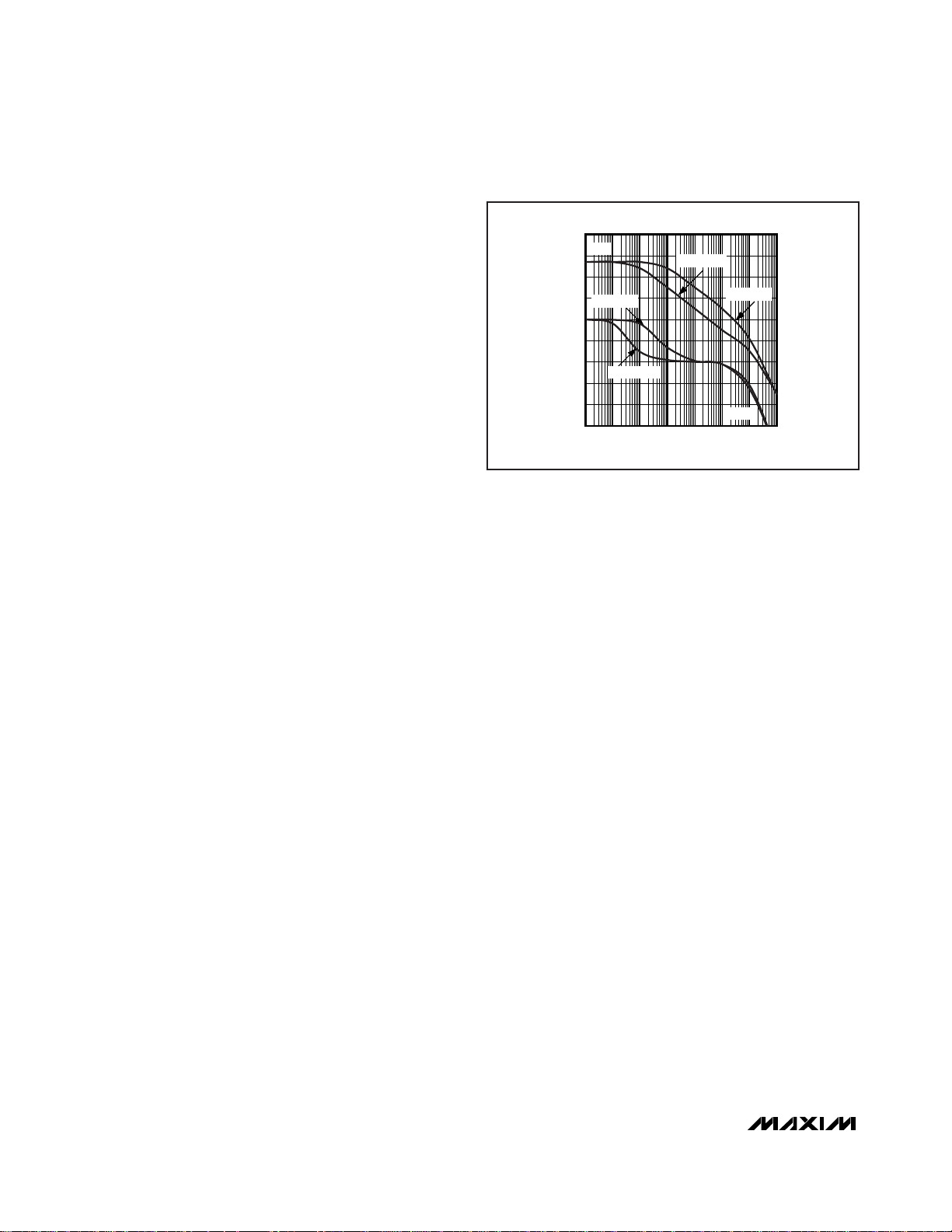
Filter Capacitor and Transient Response
In general, the choice of filter capacitor only partially
determines the time-domain response of a PA control
loop. However, some simple conventions can be
applied to affect transient response. A large filter
capacitor, C
F
, dominates time-domain response, but
the loop bandwidth remains a factor of the PA gaincontrol range. The bandwidth is maximized at power
outputs near the center of the PA’s range, and minimized at the low and high power levels, where the
slope of the gain-control curve is lowest.
A smaller valued C
F
results in an increased loop bandwidth inversely proportional to the capacitor value.
Inherent phase lag in the PA’s control path, usually
caused by parasitics at the OUT pin, ultimately results
in the addition of complex poles in the AC loop equation. To avoid this secondary effect, experimentally
determine the lowest usable C
F
for the power amplifier
of interest. This requires full consideration to the intricacies of the PA control function. The worst-case condition, where the PA output is smallest (gain function is
steepest), should be used because the PA control
function is typically nonlinear. An additional zero can
be added to improve loop dynamics by placing a resistor in series with C
F
. See Figure 3 for the gain and
phase response for different C
F
values.
Additional Input Coupling
There are three common methods for input coupling:
broadband resistive, narrowband reactive, and series
attenuation. A broadband resistive match is implemented
by connecting a resistor to ground at RFIN as shown in
Figure 4a. A 50Ω resistor (use other values for different
input impedances) in this configuration in parallel with the
input impedance of the MAX4000 presents an input
GAIN AND PHASE vs. FREQUENCY
MAX4000 fig03
FREQUENCY (Hz)
GAIN (dB)
PHASE (DEGREES)
10M1M10k 100k1k100
-80
-60
-40
-20
0
20
40
60
80
-100
-180
-135
-90
-45
0
45
90
135
180
-225
10 100M
GAIN
PHASE
CF = 2000pF
CF = 2000pF
CF = 200pF
CF = 200pF
Figure 3. Gain and Phase vs. Frequency Graph

impedance of approximately 50Ω. See the Typical
Operating Characteristics for the input impedance plot to
determine the required external termination at the frequency of interest. The MAX4001/MAX4002 require an
additional external coupling capacitor in series with the
RF input. As the operating frequency increases over
2GHz, input impedance is reduced, resulting in the need
for a larger-valued shunt resistor. Use a Smith Chart for
calculating the ideal shunt resistor value.
For high frequencies, use narrowband reactive coupling.
This implementation is shown in Figure 4b. The matching
components are drawn as reactances since these can
be either capacitors or inductors depending on the input
impedance at the desired frequency and available standard value components. A Smith Chart is used to obtain
the input impedance at the desired frequency and then
matching reactive components are chosen. Table 1 provides standard component values at some common frequencies for the MAX4001. Note that these inductors
must have a high SRF (self-resonant frequency), much
higher than the intended frequency of operation to implement this matching scheme.
Device sensitivity is increased by the use of a reactive
matching network, because a voltage gain occurs
before being applied to RFIN. The associated gain is
calculated with the following equation:
where R1 is the source impedance to which the device
is being matched, and R2 is the input resistance of the
device. The gain is the best-case scenario for a perfect
match. However, component tolerance and standard
value choice often result in a reduced gain.
Figure 4c demonstrates series attenuation coupling.
This method is intended for use in applications where
the RF input signal is greater than the input range of the
device. The input signal is thus resistively divided by
the use of a series resistor connected to the RF source.
Since the MAX4000/MAX4001/MAX4002 log amps offer
a wide selection of RF input ranges, series attenuation
coupling is not needed for typical applications.
Voltage Gain
R
R
dB
log= 20
2
1
10
MAX4000/MAX4001/MAX4002
2.5GHz 45dB RF-Detecting Controllers
______________________________________________________________________________________ 15
Table 1. Suggested Components for
MAX4001 Reactive Matching Network
(GHz)
j
X1
(nH) j
X2
(nH)
VOLTAGE
GAIN (dB)
0.9 38 47 12.8
1.9 4.4 4.7 3.2
2.5 — 1.8 -0.3
Figure 4a. Broadband Resistive Matching
MAX4000
MAX4001
MAX4002
50Ω SOURCE
50Ω
C
C
** CC*
C
IN
R
IN
V
CC
*MAX4000 ONLY INTERNALLY COUPLED
**MAX4001/MAX4002 REQUIRE EXTERNAL COUPLING
RFIN
j
X1
j
X2
Figure 4b. Narrowband Reactive Matching
MAX4000
MAX4001
MAX4002
R
ATTN
CC** CC*
C
IN
R
IN
V
CC
*MAX4000 ONLY INTERNALLY COUPLED
**MAX4001/MAX4002 REQUIRE EXTERNAL COUPLING
RFIN
STRIPLINE
Figure 4c. Series Attenuation Network
50Ω SOURCE
50Ω
R
S
50Ω
*MAX4000 ONLY INTERNALLY COUPLED
**MAX4001/MAX4002 REQUIRE EXTERNAL COUPLING
** CC*
C
C
RFIN
MAX4000
MAX4001
MAX4002
C
IN
V
CC
R
IN
FREQUENCY

MAX4000/MAX4001/MAX4002
Waveform Considerations
The MAX4000/MAX4001/MAX4002 family of log amps
respond to voltage, not power, even though input levels
are specified in dBm. It is important to realize that input
signals with identical RMS power but unique waveforms
results in different log amp outputs.
Differing signal waveforms result in either an upward or
downward shift in the logarithmic intercept. However,
the logarithmic slope remains the same.
Layout Considerations
As with any RF circuit, the layout of the MAX4000/
MAX4001/MAX4002 circuits affects performance. Use a
short 50Ω line at the input with multiple ground vias
along the length of the line. The input capacitor and
resistor should both be placed as close to the IC as
possible. V
CC
should be bypassed as close as possible to the IC with multiple vias connecting the capacitor
to the ground plane. It is recommended that good RF
components be chosen for the desired operating frequency range. Electrically isolate RF input from
other pins (especially SET) to maximize performance at high frequencies (especially at the high
power levels of the MAX4002).
UCSP Reliability
The UCSP represents a unique package that greatly
reduces board space compared to other packages.
UCSP reliability is integrally linked to the user’s assembly methods, circuit board material, and usage environment. The user should closely review these areas when
considering use of a UCSP. This form factor may not
perform equally to a packaged product through traditional mechanical reliability tests. Performance through
operating life test and moisture resistance remains
uncompromised as it is primarily determined by the
wafer fabrication process. Mechanical stress performance is a greater consideration for a UCSP. UCSP solder joint contact integrity must be considered since the
package is attached through direct solder contact to
the user’s PCB. Testing done to characterize the UCSP
reliability performance shows that it is capable of performing reliably through environmental stresses.
Results of environmental stress tests and additional
usage data and recommendations are detailed in the
UCSP application note, which can be found on Maxim’s
website, www.maxim-ic.com.
2.5GHz 45dB RF-Detecting Controllers
16 ______________________________________________________________________________________
Pin Configurations
1
2
3
4
8
7
6
5
V
CC
OUT
N.C.
GNDCLPF
A
123
B
C
SET
SHDN
RFIN
MAX4000
MAX4001
MAX4002
μMAX
TOP VIEW
RFIN SET
V
CC
CLPF
V
CC
OUT GND
SHDN
MAX4000
MAX4001
MAX4002
UCSP
TOP VIEW
(BUMPS ON BOTTOM)
Chip Information
TRANSISTOR COUNT: 358
PROCESS: Bipolar

MAX4000/MAX4001/MAX4002
2.5GHz 45dB RF-Detecting Controllers
______________________________________________________________________________________ 17
Package Information
(The package drawing(s) in this data sheet may not reflect the most current specifications. For the latest package outline information
go to www.maxim-ic.com/packages
.)
9LUCSP, 3x3.EPS
PACKAGE OUTLINE, 3x3 UCSP
1
21-0093
L
1

MAX4000/MAX4001/MAX4002
2.5GHz 45dB RF-Detecting Controllers
18 ______________________________________________________________________________________
8LUMAXD.EPS
PACKAGE OUTLINE, 8L uMAX/uSOP
1
1
21-0036
J
REV.DOCUMENT CONTROL NO.APPROVAL
PROPRIETARY INFORMATION
TITLE:
MAX
0.043
0.006
0.014
0.120
0.120
0.198
0.026
0.007
0.037
0.0207 BSC
0.0256 BSC
A2
A1
c
e
b
A
L
FRONT VIEW
SIDE VIEW
E H
0.6±0.1
0.6±0.1
Ø0.50±0.1
1
TOP VIEW
D
8
A2
0.030
BOTTOM VIEW
1
6°
S
b
L
H
E
D
e
c
0°
0.010
0.116
0.116
0.188
0.016
0.005
8
4X S
INCHES
-
A1
A
MIN
0.002
0.950.75
0.5250 BSC
0.25 0.36
2.95 3.05
2.95 3.05
4.78
0.41
0.65 BSC
5.03
0.66
6°0°
0.13 0.18
MAX
MIN
MILLIMETERS
- 1.10
0.05 0.15
α
α
DIM
Package Information (continued)
(The package drawing(s) in this data sheet may not reflect the most current specifications. For the latest package outline information
go to www.maxim-ic.com/packages
.)

MAX4000/MAX4001/MAX4002
2.5GHz 45dB RF-Detecting Controllers
Maxim cannot assume responsibility for use of any circuitry other than circuitry entirely embodied in a Maxim product. No circuit patent licenses are
implied. Maxim reserves the right to change the circuitry and specifications without notice at any time.
Maxim Integrated Products, 120 San Gabriel Drive, Sunnyvale, CA 94086 408-737-7600 ____________________ 19
© 2007 Maxim Integrated Products is a registered trademark of Maxim Integrated Products, Inc.
Revision History
REVISION
NUMBER
REVISION
DATE
DESCRIPTION
PAGES
CHANGED
1 7/02 — —
2 12/07 Insertion/correction of figures and text changes. 1, 4–13, 16
 Loading...