

Page 1
查询MAX398供应商
19-0299; Rev. 2; 7/96
Precision, 8-Channel/Dual 4-Channel,
Low-Voltage, CMOS Analog Multiplexers
_______________General Description
The MAX398/MAX399 precision, monolithic, CMOS analog multiplexers (muxes) offer low on-resistance (less
than 100Ω), which is matched to within 6Ω between
channels and remains flat over the specified analog signal range (11Ω max). They also offer low leakage over
temperature (NO-off leakage current less than 2.5nA at
+85°C) and fast switching speeds (transition time less
than 250ns). The MAX398 is an 8-channel device, and
the MAX399 is a dual 4-channel device.
The MAX398/MAX399 are fabricated with Maxim’s lowvoltage silicon-gate process. Design improvements
yield extremely low charge injection (less than 5pC) and
guarantee electrostatic discharge protection greater than
2000V.
These muxes operate with a single +3V to +15V supply or
bipolar ±3V to ±8V supplies, while retaining CMOS-logic
input compatibility and fast switching. CMOS inputs provide reduced input loading. The MAX398/MAX399 are
pin compatible with the industry-standard DG408,
DG409, DG508A, and DG509A.
________________________Applications
Sample-and-Hold Circuits
Automatic Test Equipment
Heads-Up Displays
Guidance and Control Systems
Military Radios
Communications Systems
Battery-Operated Systems
PBX, PABX
Audio Signal Routing
Low-Voltage Data Acquisition Systems
____________________________Features
♦ Pin Compatible with Industry-Standard
DG408/DG409/DG508A/DG509A
♦ Guaranteed On-Resistance Match
Between Channels (<6Ω )
♦ Low On-Resistance (<100Ω )
♦ Guaranteed Flat On-Resistance over Signal
Range (<11Ω)
♦ Guaranteed Low Charge Injection (<5pC)
♦ NO-Off Leakage Current <1nA at +85°C
♦ COM-Off Leakage Current <2.5nA at +85°C
♦ Electrostatic Discharge Protection >2000V
♦ Single-Supply Operation (+3V to +15V)
Bipolar-Supply Operation (±3V to ±8V)
♦ Low Power Consumption (<300µW)
♦ Rail-to-Rail Signal Handling
♦ TTL/CMOS-Logic Compatible
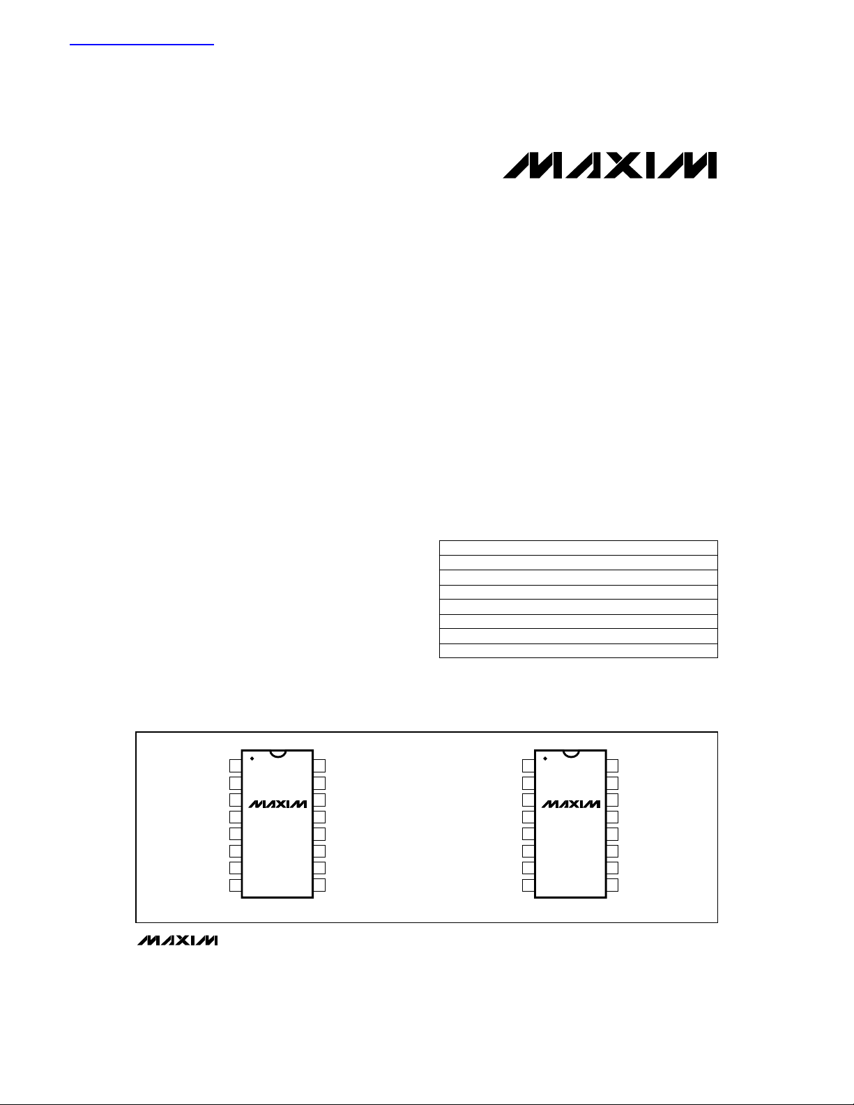
______________Ordering Information
PART
MAX398CPE
MAX398CSE
MAX398C/D 0°C to +70°C
MAX398EPE
MAX398ESE -40°C to +85°C
MAX398EJE
MAX398MJE -55°C to +125°C
Ordering Information continued at end of data sheet.
* Contact factory for dice specifications.
** Contact factory for package availability.
TEMP. RANGE PIN-PACKAGE
0°C to +70°C
0°C to +70°C
-40°C to +85°C 16 Plastic DIP
-40°C to +85°C 16 CERDIP**
16 Plastic DIP
16 Narrow SO
Dice*
16 Narrow SO
16 CERDIP**
__________________________________________________________Pin Configurations
MAX398/MAX399
TOP VIEW
A0
1
EN
2
V-
3
N01
N02
N03
N04
COM
MAX398
4
5
6
7
8
DIP/SO
________________________________________________________________
A1
16
A2
15
GND
14
V+
13
NO5
12
NO6
11
NO7
10
NO8
9
N01A
N02A
N03A
N04A
COMA
A0
1
EN
2
V-
3
MAX399
4
5
6
7
8
DIP/SO
Maxim Integrated Products
A1
16
GND
15
V+
14
NO1B
13
NO2B
12
NO3B
11
NO4B
10
COMB
9
1
For free samples & the latest literature: http://www.maxim-ic.com, or phone 1-800-998-8800
Page 2
Precision, 8-Channel/Dual 4-Channel,
Low-Voltage, CMOS Analog Multiplexers
ABSOLUTE MAXIMUM RATINGS
Voltage Referenced to GND
V+.......................................................................-0.3V to +17V
V-........................................................................+0.3V to -17V
V+ to V-...............................................................-0.3V to +17V
Voltage into Any Terminal (Note 1).........(V- - 2V) to (V+ + 2V) or
30mA (whichever occurs first)
Current into Any Terminal ...................................................30mA
Peak Current, Any Terminal
(pulsed at 1ms, 10% duty cycle max) ............................40mA
Continuous Power Dissipation (T
Plastic DIP (derate 7.5mW/°C above +70°C) ..............470mW
Narrow SO (derate 8.7mW/°C above +70°C) ..............696mW
CERDIP (derate 10.0mW/°C above +70°C).................900mW
Operating Temperature Ranges
MAX39_C_ _ .......................................................0°C to +70°C
MAX39_E_ _.....................................................-40°C to +85°C
MAX39_MJE ..................................................-55°C to +125°C
Storage Temperature Range.............................-65°C to +150°C
Lead Temperature (soldering, 10sec).............................+300°C
Note 1: Signals on any terminal exceeding V+ or V- are clamped by internal diodes. Limit forward current to maximum current ratings.
Stresses beyond those listed under “Absolute Maximum Ratings” may cause permanent damage to the device. These are stress ratings only, and functional
operation of the device at these or any other conditions beyond those indicated in the operational sections of the specifications is not implied. Exposure to
absolute maximum rating conditions for extended periods may affect device reliability.
= +70°C)
A
MAX398/MAX399
ELECTRICAL CHARACTERISTICS—Dual Supplies
(V+ = +5V ±10%, V- = -5V ±10%, GND = 0V, VAH= V
SYMBOLPARAMETER
SWITCH
Analog Signal Range
Channel On-Resistance
RONMatching Between
Channels (Note 4)
On-Resistance Flatness
(Note 5)
NO-Off Leakage Current
(Note 6)
COM-Off Leakage Current
(Note 6)
COM-On Leakage Current
(Note 6)
, V
COM
R
ON
∆R
ON
R
FLAT(ON)
I
NO(OFF)
I
COM(OFF)
I
COM(ON)
(Note 3)
NO
INO= 1mA, V
INO= 1mA, V
V+ = 5V, V- = -5V
INO= 1mA, V
V+ = 5V, V- = -5V
VNO= ±4.5V, V
V+ = 5.5V, V- = -5.5V
V
COM
V
NO
V+ = 5.5V, V- = -5.5V
V
COM
V
NO
V+ = 5.5V, V- = -5.5V
V
COM
V
NO
ENH
= ±4.5V,
±
= 4.5V,
= ±4.5V,
±
= 4.5V,
= ±4.5V,
= 4.5V,
= +2.4V, VAL= V
CONDITIONS
= ±3.5V
COM
= ±3.5V,
COM
= ±3V,
COM
±
= 4.5V,
COM
MAX398
MAX399
MAX398
MAX399
= +0.8V, TA= T
ENL
TA= +25°C
TA= T
MIN
TA= +25°C
TA= T
MIN
TA= +25°C
TA= T
MIN
TA= +25°C
TA= T
MIN
to T
MAX
TA= +25°C
TA= T
MIN
to T
MAX
TA= +25°C
TA= T
MIN
to T
MAX
TA= +25°C
TA= T
MIN
to T
MAX
TA= +25°C
TA= T
MIN
to T
MAX
to T
to T
to T
MAX
MAX
MAX
C, E
M
C, E
M
C, E
M
C, E
M
C, E
M
MIN
to T
, unless otherwise noted.)
MAX
MIN TYP MAX
(Note 2)
60 100
125
6
8
11
14
-0.1 0.1
-1.0 1.0
-10 10
-0.2 0.2
-2.5 2.5
-20 20
-0.1 0.1
-1.5 1.5
-10 10
-0.4 0.4
-5 5
-40 40
-0.2 0.2
-2.5 2.5
-20 20
UNITS
VV- V+V
Ω
Ω
Ω
nA
nA
nA
2 _______________________________________________________________________________________
Page 3
Precision, 8-Channel/Dual 4-Channel,
Low-Voltage, CMOS Analog Multiplexers
ELECTRICAL CHARACTERISTICS—Dual Supplies (continued)
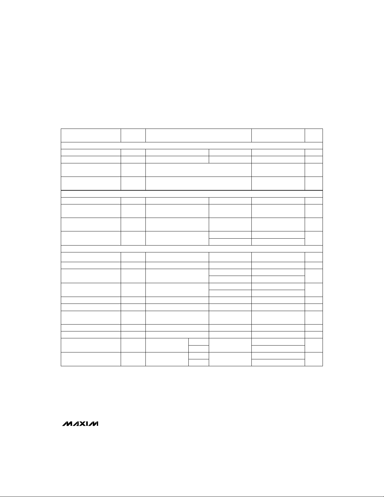
(V+ = +5V ±10%, V- = -5V ±10%, GND = 0V, VAH= V
SYMBOLPARAMETER
DIGITAL LOGIC INPUT
Logic High Input Voltage
Logic Low Input Voltage TA= T
Input Current with
Input Voltage High
Input Current with
Input Voltage Low
ENH
ENL
ENH
ENL
VA= VEN= 2.4V µA-0.1 0.1IAH, I
SUPPLY
VEN= VA= 0V/V+,
V+ = 5.5V, V- = -5.5V
VEN= VA= 0V/V+,
V+ = 5.5V, V- = -5.5V
Ground Current
I
VEN= VA= 0V/V+,
GND
V+ = 5.5V, V- = -5.5V
DYNAMIC
Transition Time
Break-Before-Make Interval
Enable Turn-On Time
Enable Turn-Off Time
TRANS
t
ON(EN)
t
OFF(EN)
OPEN
Figure1
Figure 2
Figure 3
Figure 3
CL= 10nF, VS= 0V, RS= 0Ω
VEN= 0V, RL= 1kΩ, f = 100kHz
Crosstalk Between Channels
Logic Input Capacitance
NO-Off Capacitance
COM-Off Capacitance pF
COM-On Capacitance pF
NO(OFF)
C
COM(OFF)
C
COM(ON)
VEN= 2.4V, f = 100kHz,
CT
V
GEN
f = 1MHz
IN
f = 1MHz, VEN= VD= 0V
f = 1MHz,
VEN= VD= 0V
f = 1MHz,
VEN= VD= 0V
= 1V
ENH
p-p
= +2.4V, VAL= V
CONDITIONS
, RL= 1kΩ
MAX398
MAX399
MAX398
MAX399
= +0.8V, TA= T
ENL
TA= T
MIN
MIN
TA= +25°C
TA= T
MIN
TA= +25°C
TA= T
MIN
TA= +25°C
TA= +25°C
TA= T
MIN
TA= +25°C
TA= T
MIN
TA= +25°C
TA= +25°C
TA= +25°C
TA= +25°C
TA= +25°C
TA= +25°C
TA= +25°C
to T
to T
to T
to T
to T
to T
MAX
MAX
MAX
MAX
MAX
MAX
MIN
to T
, unless otherwise noted.)
MAX
MIN TYP MAX
(Note 2)
-0.1 0.1IAL, I
-1 1
-1 1
60 150
250
40 150
200
40
20
54
34
MAX398/MAX399
UNITS
V2.4VAH, V
V0.8VAL, V
µAVA= VEN= 0.8V
V±3 ±8Power-Supply Range
µA-1 1I+Positive Supply Current
µA-1 1I-Negative Supply Current
µA
ns150t
ns040t
ns
ns
pC25QCharge Injection (Note 3)
dB-75Off Isolation (Note 7)
dB-92V
pF8C
pF11C
_______________________________________________________________________________________ 3
Page 4
Precision, 8-Channel/Dual 4-Channel,
Low-Voltage, CMOS Analog Multiplexers
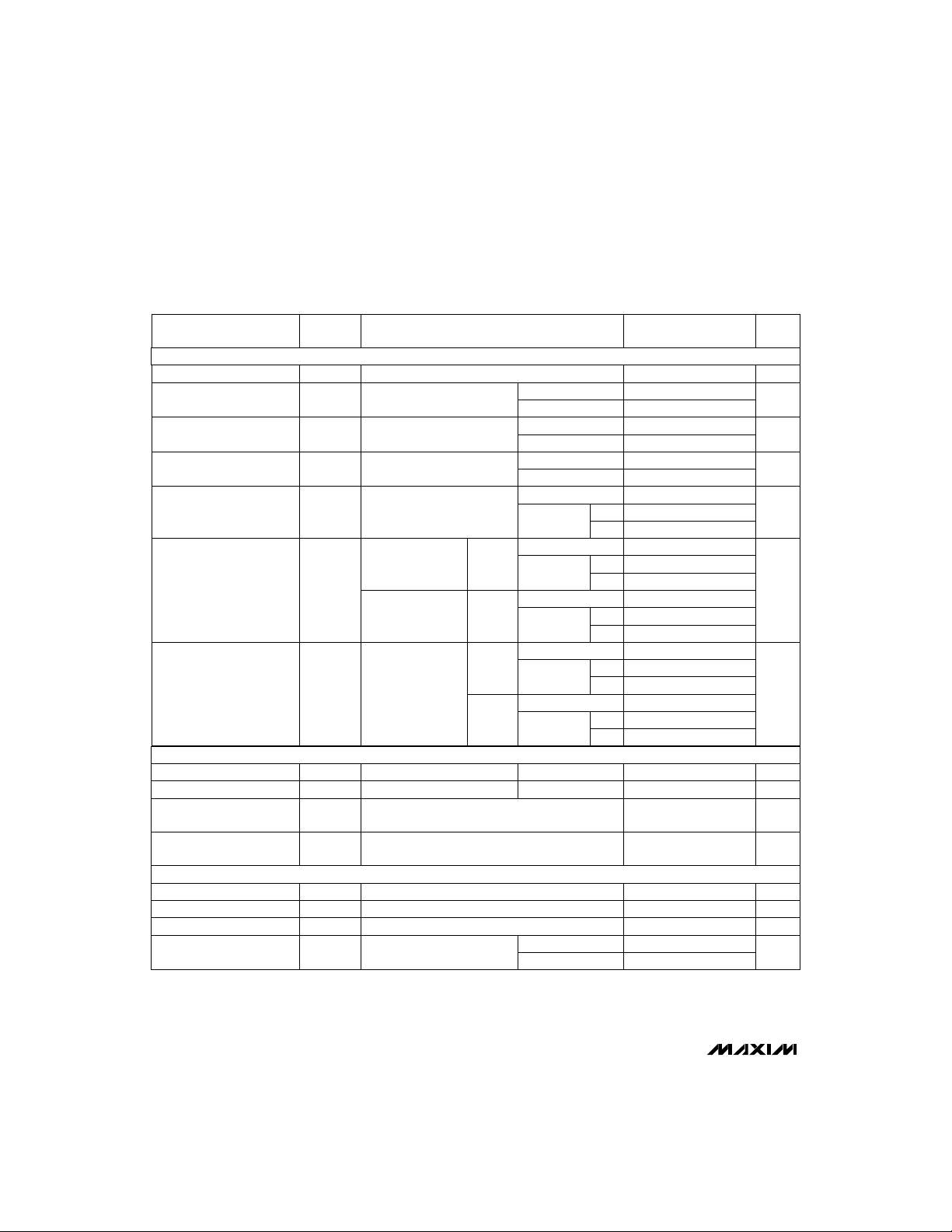
ELECTRICAL CHARACTERISTICS—Single 5V
(V+ = 5V ±10%, V- = 0V, GND = 0V, VAH= V
SYMBOLPARAMETER
SWITCH
Analog Signal Range
On-Resistance
RONMatching Between
Channels (Note 4)
On-Resistance Flatness
NO-Off Leakage Current
MAX398/MAX399
(Note 8)
COM-Off Leakage Current
(Note 8)
COM-On Leakage Current
(Note 8)
, V
COM
R
ON
∆R
ON
R
FLAT
I
NO(OFF)
I
COM(OFF)
I
COM(ON)
NO
DIGITAL LOGIC INPUT
Logic High Input Voltage
Logic Low Input Voltage
Input Current with
Input Voltage High
Input Current with
Input Voltage Low
IAL, I
ENH
ENL
ENH
ENL
SUPPLY
I
GND Supply Current
I
GND
= +2.4V, VAL= V
ENH
= +0.8V, TA= T
ENL
CONDITIONS
(Note 3)
INO= 1mA, V
V+ = 4.5V
INO= 1mA, V
V+ = 4.5V
INO= 1mA; V
V+ = 5V
VNO= 4.5V, V
V+ = 5.5V
V
= 4.5V,
COM
V
= 0V,
NO
V+ = 5.5V
V
= 4.5V,
COM
V
= 0V,
NO
V+ = 5.5V
= 3.5V,
COM
= 3.5V,
COM
= 3V, 2V, 1V;
COM
COM
= 0V,
MAX398
MAX399
TA= +25°C
TA= T
TA= +25°C
TA= T
TA= +25°C
TA= T
TA= +25°C
TA= T
to T
MAX
TA= +25°C
TA= T
to T
MAX
TA= +25°C
TA= T
to T
MAX
TA= +25°C
V
= 4.5V,
COM
V
= 4.5V,
NO
V+ = 5.5V
MAX398
MAX399
TA= T
to T
MAX
TA= +25°C
TA= T
to T
MAX
TA= T
VA= VEN= 2.4V µA-0.1 0.1IAH, I
VA= 0V
VEN= 0.8V
VEN= VA= 0V, V+; V+ = 5.5V; V- = 0V
VEN= VA= 0V, V+; V+ = 5.5V; V- = 0V
VEN= V+, 0V; VA= 0V;
V+ = 5.5V; V- = 0V
TA= +25°C
TA= T
MIN
MIN
MIN
MIN
MIN
MIN
MIN
MIN
MIN
MIN
MIN
MIN
to T
to T
to T
to T
to T
to T
to T
, unless otherwise noted.)
MAX
MIN TYP MAX
MAX
MAX
MAX
-0.1 0.1
-1.0 1.0
C, E
-10 10
M
-0.2 0.2
-2.5 2.5
C, E
-20 20
M
-0.2 0.2
-1.5 1.5
C, E
-10 10
M
-0.4 0.4
C, E
M
-5 5
-40 40
-0.2 0.2
-2.5 2.5
C, E
-20 20
M
MAX
MAX
-0.1 0.1
-1.0 1.0
-1.0 1.0
MAX
(Note 2)
150 225
10 18
15 22
280
11
13
0.8VAL, V
UNITS
VV- V+V
Ω
Ω
Ω
nA
nA
nA
V2.4VAH, V
VTA= T
µA
V315Power-Supply Range
µA-1.0 1.0I+Positive Supply Current
µA-1.0 1.0I-Negative Supply Current
µA
4 _______________________________________________________________________________________
Page 5

Precision, 8-Channel/Dual 4-Channel,
Low-Voltage, CMOS Analog Multiplexers
ELECTRICAL CHARACTERISTICS—Single 5V (continued)
(V+ = 5V ±10%, V- = 0V, GND = 0V, VAH= V
SYMBOLPARAMETER
DYNAMIC
Transition Time
Break-Before-Make Interval
Enable Turn-On Time
Enable Turn-Off Time
TRANS
t
OPEN
t
ON(EN)
t
OFF(EN)
= +2.4V, VAL= V
ENH
ENL
CONDITIONS
VNO= 3V
CL= 10nF, VS= 0V, RS= 0Ω
= +0.8V, TA= T
TA= +25°C
TA= +25°C
TA= T
MIN
TA= +25°C
TA= T
MIN
TA= +25°C
ELECTRICAL CHARACTERISTICS—Single 3V
(V+ = 3V ±10%, V- = 0V, GND = 0V, VAH= V
SYMBOLPARAMETER
SWITCH
Analog Signal Range
On-Resistance
ANALOG
R
ON
DYNAMIC
Transition Time (Note 3)
Enable Turn-On Time (Note 3)
Enable Turn-Off Time (Note 3)
TRANS
ON(EN)
OFF(EN)
= +2.4V, VAL= V
ENH
ENL
CONDITIONS
(Note 3)
INO= 1mA, V
V+ = 3V
COM
= 1.5V,
Figure 1, VIN= 2.4V,
V
= 1.5V, V
N01
Figure 3, V
V
= 0V, V
INL
Figure 3, V
V
= 0V, V
INL
INH
INH
N01
N01
= 0V
N08
= 2.4V,
= 1.5V
= 2.4V,
= 1.5V
CL= 10nF, VS= 0V, RS= 0Ω
= +0.8V, TA= T
TA= +25°C
TA= T
MIN
TA= +25°C
TA= +25°C
TA= +25°C
TA= +25°C
MIN
to T
to T
MIN
to T
to T
, unless otherwise noted.)
MAX
MIN TYP MAX
MAX
MAX
to T
, unless otherwise noted.)
MAX
MIN TYP MAX
MAX
(Note 2)
90 200
50 125
(Note 2)
230 375
75 400t
275
200
425
MAX398/MAX399
UNITS
ns90 245t
ns10 40
ns
ns
pC1.5 5QCharge Injection (Note 3)
UNITS
VV- V+V
Ω
ns230 575t
ns200 500t
ns
pC15QCharge Injection (Note 3)
Note 2: The algebraic convention, where the most negative value is a minimum and the most positive value a maximum, is used in
this data sheet.
Note 3: Guaranteed by design.
Note 4: ∆R
Note 5: Flatness is defined as the difference between the maximum and minimum value of on-resistance as measured over the
Note 6: Leakage parameters are 100% tested at maximum rated hot operating temperature, and guaranteed by correlation at +25°C.
Note 7: Worst-case isolation is on channel 4 because of its proximity to the COM pin. Off isolation = 20log V
Note 8: Leakage testing at single supply is guaranteed by correlation testing with dual supplies.
= RONMAX - RONMIN.
ON
specified analog signal ranges, i.e., V
= input to off switch.
V
NO
= 3V to 0V and 0V to -3V.
NO
COM/VNO
, V
COM
= output,
_______________________________________________________________________________________ 5
Page 6

Precision, 8-Channel/Dual 4-Channel,
Low-Voltage, CMOS Analog Multiplexers
__________________________________________Typical Operating Characteristics
(TA = +25°C, unless otherwise noted.)
ON-RESISTANCE vs. V
(DUAL SUPPLIES)
110
100
90
80
(Ω)
70
ON
R
60
50
40
MAX398/MAX399
30
-5 -3 1
-1 3
V
ON-RESISTANCE vs. V
AND TEMPERATURE
180
160
140
120
(Ω)
ON
100
R
80
60
40
02
(SINGLE SUPPLY)
V+ = 5V
V- = 0V
TA = +125°C
T
153
V
COM
V± = ±3V
V± = ±5V
COM
TA = +85°C
TA = -55°C
4
5-4 0-2 2 4
(V)
COM
= +25°C
A
(V)
COM
CHARGE INJECTION vs. V
5
V+ = 5V
V- = 0V
Qj (pC)
110
100
MAX398/9 TOC1
(Ω)
ON
R
1000
MAX398/9 TOC4
OFF-LEAKAGE (pA)
COM
ON-RESISTANCE vs. V
AND TEMPERATURE
(DUAL SUPPLIES)
V+ = 5V
V- = -5V
90
V+ = 5.5V
V- = -5.5V
MAX398/9 TOC7
TA = +125°C
TA = +85°C
TA = +25°C
TA = -55°C
-1 3
V
COM
OFF-LEAKAGE vs.
TEMPERATURE
TEMPERATURE (°C)
80
70
60
50
40
30
-5 -3 1
100
10
1
0.1
-50 12525-25 0 7550 100
(V)
COM
10
1
I+, I- (nA)
MAX398/9 TOC2
5-4 0-2 2 4
MAX398/9 TOC5
V+ = 5V
V- = -5V
V
EN
300
275
250
225
200
(Ω)
175
ON
R
150
125
100
10,000
1000
ON-LEAKAGE (pA)
= VA = 0V, 5V
ON-RESISTANCE vs. V
(SINGLE SUPPLY)
V- = 0V
V+ = 3V
75
50
02
153
V
(V)
COM
ON-LEAKAGE vs.
TEMPERATURE
V+ = 5.5V
V- = -5.5V
100
10
1
0.1
-50 12525-25 0 7550 100
TEMPERATURE (°C)
SUPPLY CURRENT vs.
TEMPERATURE
I+
I-
V+ = 5V
MAX398/9 TOC7
COM
MAX398/9 TOC3
4
MAX398/9 TOC6
V+ = 5V
V- = -5V
-5
-5 -3 1
-1 305-4 0-2 2 4
V
(V)
COM
0.1
-50 12525-25 0 7550 100
TEMPERATURE (°C)
6 _______________________________________________________________________________________
Page 7

Precision, 8-Channel/Dual 4-Channel,
Low-Voltage, CMOS Analog Multiplexers
______________________________________________________________Pin Description
PIN
MAX398 MAX399
1, 15, 16 A0, A2, A1 Address Inputs
—
2 2 EN Enable Input, connect to V+ if not used
3 3 V- Negative Supply Voltage Input
4–7 — NO1–NO4 Analog Inputs—bidirectional
— 4–7 NO1A–NO4A Analog Inputs—bidirectional
8 — COM Analog Output—bidirectional
— 8, 9 COMA, COMB Analog Outputs—bidirectional
9–12 — NO8–NO5 Analog Inputs—bidirectional
— 10–13 NO4B–NO1B Analog Inputs—bidirectional
13 14 V+ Positive Supply Voltage Input
14 15 GND Ground
—
1, 16
NAME FUNCTION
A0, A1 Address Inputs
MAX398/MAX399
_______________________________________________________________________________________
7
Page 8

Precision, 8-Channel/Dual 4-Channel,
Low-Voltage, CMOS Analog Multiplexers
__________Applications Information
Operation with Supply Voltages
Using supply voltages less than ±5V reduces the analog
signal range. The MAX398/MAX399 muxes operate with
±3V to ±8V bipolar supplies or with a +3V to +15V single
supply. Connect V- to GND when operating with a single
supply. Both device types can also operate with unbalanced supplies, such as +10V and -5V. The
Operating Characteristics
graphs show typical on-resis-
Other than ±5V
Typical
COM
+5V
D1
V+
MAX398
MAX399
*
*
*
NO
*
tance with ±3V, ±5V, +3V and +5V supplies. (Switching
times increase by a factor of two or more for operation at
5V.)
Overvoltage Protection
Proper power-supply sequencing is recommended for
MAX398/MAX399
all CMOS devices. Do not exceed the absolute maximum ratings, because stresses beyond the listed rat-
Figure 1. Overvoltage Protection Using External Blocking Diodes
V-
D2
* INTERNAL PROTECTION DIODES
-5V
ings can cause permanent damage to the devices.
Always sequence V+ on first, then V-, followed by the
logic inputs, NO, or COM. If power-supply sequencing
is not possible, add two small signal diodes (D1, D2) in
series with supply pins for overvoltage protection
(Figure 1). Adding diodes reduces the analog signal
range to one diode drop below V+ and one diode drop
above V-, but does not affect the devices’ low switch
resistance and low leakage characteristics. Device
operation is unchanged, and the difference between
V+ and V- should not exceed 17V. These protection
diodes are not recommended when using a single supply.
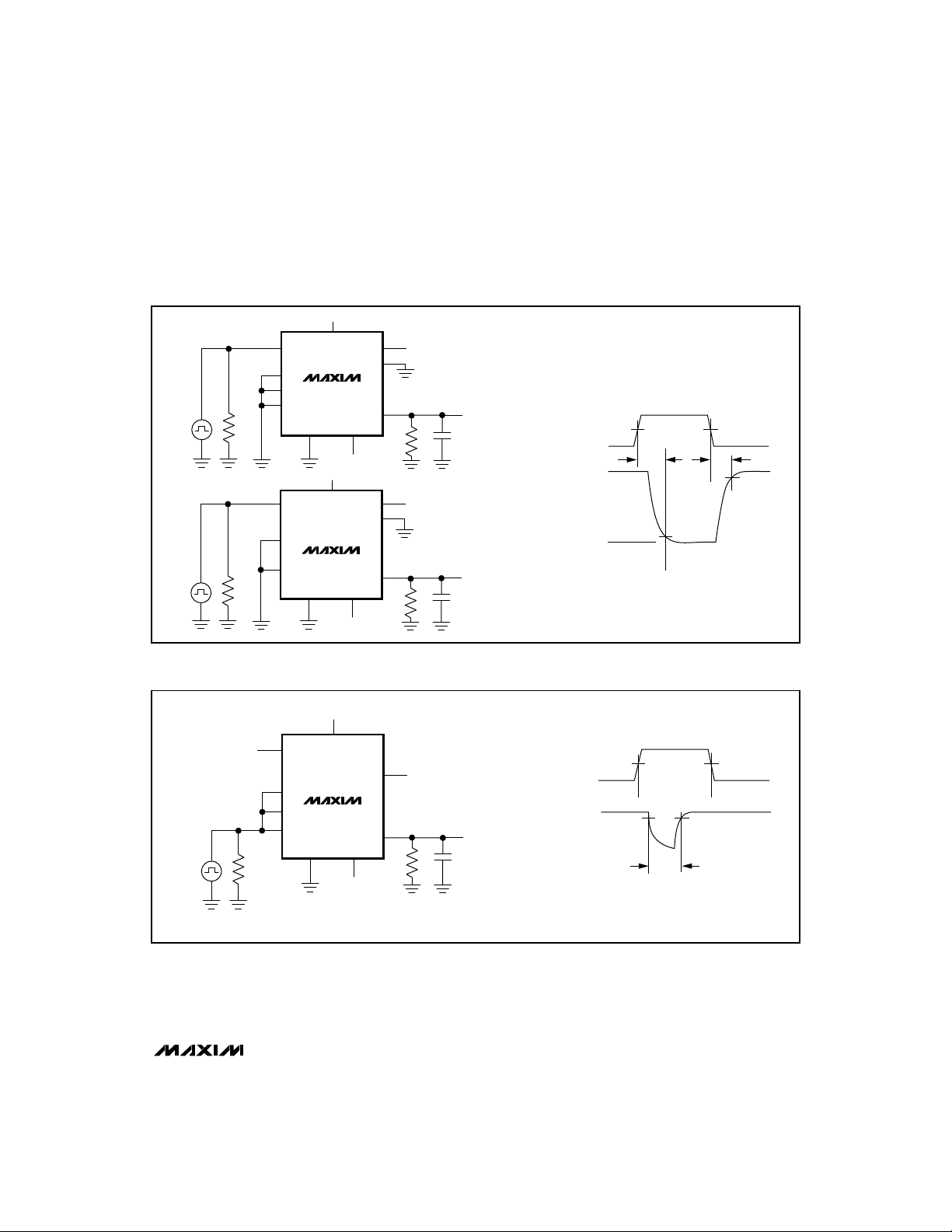
______________________________________________Test Circuits/Timing Diagrams
+5V
V+
+5V
V+
NO1A-NO4A
NO1
NO2-NO7
NO8
COM
V-
-5V
NO1B
NO4B
COMB
V-
-5V
300Ω
300Ω
+5V
-5V
+5V
-5V
35pF
35pF
LOGIC
V
OUT
V
OUT
INPUT
V
EN
SWITCH
OUTPUT
V
OUT
+3V
0V
V
NO1
0V
V
NO8
t
TRANS
ON
50%
90%
tR < 20ns
tF < 20ns
90%
t
TRANS
50Ω
50Ω
A2
A1
A0
MAX398
V
EN
EN
GND
A1
A0
MAX399
V
EN
EN
GND
Figure 2. Transition Time
8 _______________________________________________________________________________________
Page 9
Precision, 8-Channel/Dual 4-Channel,
Low-Voltage, CMOS Analog Multiplexers
_________________________________Test Circuits/Timing Diagrams (continued)
+5V
V
EN
50Ω
V
EN
50Ω
Figure 3. Enable Switching Time
V+
EN
A0
A1
MAX398
A2
GND
EN
A0
MAX399
A1
GND
NO2-NO8
-5V
+5V
V+
NO1A-NO4A
NO2B-NO4B,
-5V
+5V
V-
COMA
COMB
V-
NO1
COM
NO1B
+5V
V
OUT
+5V
35pF
35pF
V
OUT
1k
1k
LOGIC
INPUT
V
EN
SWITCH
OUTPUT
V
OUT
+3V
t
ON(EN)
50%
0V
0V
90%
tR < 20ns
tF < 20ns
10%
t
OFF(EN)
MAX398/MAX399
V
EN
+2.4V
V
A
50Ω
EN
A0
A1
MAX398
A2
GND
Figure 4. Break-Before-Make Interval
_______________________________________________________________________________________ 9
V+
NO1-NO8
COM
V-
-5V
300Ω
+5V
35pF
80%
t
OPEN
tR < 20ns
tF < 20ns
+3V
LOGIC
INPUT
0V
V
A
+5V
V
OUT
SWITCH
OUTPUT
V
OUT
0V
50%
Page 10

Precision, 8-Channel/Dual 4-Channel,
Low-Voltage, CMOS Analog Multiplexers
_________________________________Test Circuits/Timing Diagrams (continued)
+5V
R
S
V
EN
V
S
CHANNEL
SELECT
MAX398/MAX399
Figure 5. Charge Injection
+5V
V+
NO
EN
MAX398
A0
A1
A2
GND
10nF
COM
V-
-5V
V
OUT
CL = 1000nF
LOGIC
INPUT
V
EN
V
OUT
+3V
0V
IS THE MEASURED VOLTAGE DUE TO CHARGE TRANSFER
∆V
OUT
ERROR Q WHEN THE CHANNEL TURNS OFF.
Q = ∆V
OUT x CL
ONOFF OFF
+5V
10nF
∆V
OUT
V+
A0
A1
A2
NO1
NO8
GND
MAX398
EN
10nF
COM
R
= 1kΩ
V-
-5V
OFF ISOLATION = 20log
L
V
IN
R = 1kΩ
V
OUT
V
OUT
V
IN
R
= 50Ω
G
V
IN
= 50Ω
R
S
NO1
NO2
NO8
A0
A1
A2
GND
V+
MAX398
EN
10nF
Figure 6. Off Isolation Figure 7. Crosstalk
+5V
V+
CHANNEL
SELECT
A2
A1
MAX398
A0
GND
NO1
NO8
COM
EN
V-
-5V
1MHz
CAPACITANCE
ANALYZER
f = 1MHz
Figure 8. NO/COM Capacitance
10 ______________________________________________________________________________________
COM
RL = 1kΩ
V-
-5V
CROSSTALK = 20log
V
OUT
V
OUT
V
IN
Page 11

Precision, 8-Channel/Dual 4-Channel,
Low-Voltage, CMOS Analog Multiplexers
__________________________________________Functional Diagrams/Truth Tables
MAX398
NO1
NO2
NO3
NO4
NO5
NO6
NO7
NO8
V+ V- GND
DECODERS / DRIVERS
A0 A1 A2 EN
MAX398 MAX399
A2 A1 A0 EN ON SWITCH
X
X
X
0
0
0
0
0
0
1
1
1
1
0
0
1
1
0
1
1
0
0
0
1
1
0
1
1
NONE
1
1
1
2
1
3
1
4
1
5
1
6
1
7
1
8
COM
MAX399
NO1A
NO2A
NO3A
NO4A
NO1B
NO2B
NO3B
NO4B
V+ V- GND
DECODERS / DRIVERS
A0 A1 EN
A1 A0 EN ON SWITCH
X
X
0
0
0
0
1
1
0
1
1
LOGIC "O" VAL ≤ +0.8 V, LOGIC "1" VAH ≥ +2.4 V
NONE
1
1
1
2
1
3
1
4
COMA
COMB
MAX398/MAX399
______________________________________________________________________________________ 11
Page 12

Precision, 8-Channel/Dual 4-Channel,
Precision, 8-Channel/Dual 4-Channel,
Low-Voltage, CMOS Analog Multiplexers
Low-Voltage, CMOS Analog Multiplexers
_Ordering Information (continued)
PART
MAX399CPE
MAX399CSE
MAX399EPE
MAX399EJE
* Contact factory for dice specifications.
** Contact factory for package availability.
__________________________________________________________Chip Topographies
MAX398/MAX399
MAX398/MAX399
0°C to +70°C
0°C to +70°C
0°C to +70°CMAX399C/D
-40°C to +85°CMAX399ESE
-55°C to +125°CMAX399MJE
PIN-PACKAGETEMP. RANGE
16 Plastic DIP
16 Narrow SO
Dice*
16 Plastic DIP-40°C to +85°C
16 Narrow SO
16 CERDIP**-40°C to +85°C
16 CERDIP**
MAX398
EN
A0 A1 A2 GND
V-
NO1
NO2
NO3
NO4
COM NO8
0.080"
(2.03mm)
TRANSISTOR COUNT: 161
SUBSTRATE CONNECTED TO V+
V+
NO5
NO6
N.C.
NO7
0.102"
(2.59mm)
MAX399
EN
A0 A1 N.C. GND
V-
NO1A
NO2A
NO3A
NO4A
COMA COMB
0.080"
(2.03mm)
TRANSISTOR COUNT: 161
SUBSTRATE CONNECTED TO V+
V+
NO1B
NO2B
NO3B
NO4B
0.102"
(2.59mm)
Maxim cannot assume responsibility for use of any circuitry other than circuitry entirely embodied in a Maxim product. No circuit patent licenses are
implied. Maxim reserves the right to change the circuitry and specifications without notice at any time.
12
__________________Maxim Integrated Products, 120 San Gabriel Drive, Sunnyvale, CA 94086 (408) 737-7600
© 1996 Maxim Integrated Products Printed USA is a registered trademark of Maxim Integrated Products.
 Loading...