

Page 1

19-4973; Rev 2; 4/12
EVALUATION KIT
AVAILABLE
8.5Gbps Quad Equalizer and
Preemphasis Driver
General Description
The MAX3987 is a 4-channel receive and transmit equalizer (EQ). It compensates for transmission medium
losses encountered with FR4 stripline/microstrip and/or
high-speed cable. The device can be used at the beginning, middle, or end of a channel. The input equalization
requires no setting, and the output preemphasis (PE) is
programmable.
For each channel, the preemphasis level, output drive
level, output polarity, and powering down of unused outputs are programmable through an I2C serial interface. It
can also be configured globally through pins.
The device operates from a 2.5V or 3.3V supply, and is
packaged in a 7mm x 7mm, 48-pin TQFN.
Applications
Preemphasis and Receive Equalization
Redrive
FR4 and Cable Equalization
XAUI and XAUI2, Fibre Channel, Interlaken,
InfiniBand
TM/SM
, SAS-2 and SATA Revision 3 OOB
PCIe® Compatible
InfiniBand is a trademark/service mark of InfiniBand Trade
Association.
PCIe is a registered trademark of PCI-SIG Corp.
Typical Application Circuit
Features
S Up to 8.5Gbps NRZ Data Speed
S Receive Equalization Up to 30in FR4
S Preemphasis Drive Up to 30in FR4
S Global and Individual Programming of
Preemphasis, Output Drive Levels, Polarity
Inversion, and Offset Cancellation
S Signal Detect and Internal Output Squelch
S Compliant with SAS-2 and SATA Revision 3 OOB
S Coding Independent, 8B/10B, 64B/66B,
Scrambled, and Others
S Differential CML Data-Output Drive
S I2C Serial Interface and Pin Programmable
S Software Power-Down of Unused Outputs
S 0.5W Typical Power Dissipation for Drive Level 1
at VCC = 2.5V
S High-Performance, Lead-Free, 7mm x 7mm, 48-Pin
TQFN Package
Ordering Information
PART TEMP RANGE PIN-PACKAGE
MAX3987ETM+
+Denotes a lead(Pb)-free/RoHS-compliant package.
*EP = Exposed pad.
-40NC to +85NC
48 TQFN-EP*
MAX3987
MAX3987
FABRIC
CARD
Rx Tx
SerDes SerDes
2in < L < 30in
_______________________________________________________________ Maxim Integrated Products 1
AS AN
EQUALIZER
MAX3987
AS A DRIVER
BACKPLANE
MIDPLANE
2in < L < 30in
LINE
CARD
RxTx
For pricing, delivery, and ordering information, please contact Maxim Direct at 1-888-629-4642,
or visit Maxim’s website at www.maxim-ic.com.
Page 2
8.5Gbps Quad Equalizer and
Preemphasis Drive
ABSOLUTE MAXIMUM RATINGS
Termination Supply Voltage Range .....................-0.5V to +3.9V
Signal Voltage Range on Any One
Signal Wire (TTL) ................................. -0.5V to (VCC + 0.3V)
Signal Voltage Range on Any One
Signal Wire (CML) ................................ -0.5V to (VCC + 0.3V)
CML Output Loading (Shorted to Ground) ........................90mA
Operating Ambient Temperature Range ........... -40NC to +85NC
MAX3987
Stresses beyond those listed under “Absolute Maximum Ratings” may cause permanent damage to the device. These are stress ratings only, and functional
operation of the device at these or any other conditions beyond those indicated in the operational sections of the specifications is not implied. Exposure to absolute
maximum rating conditions for extended periods may affect device reliability.
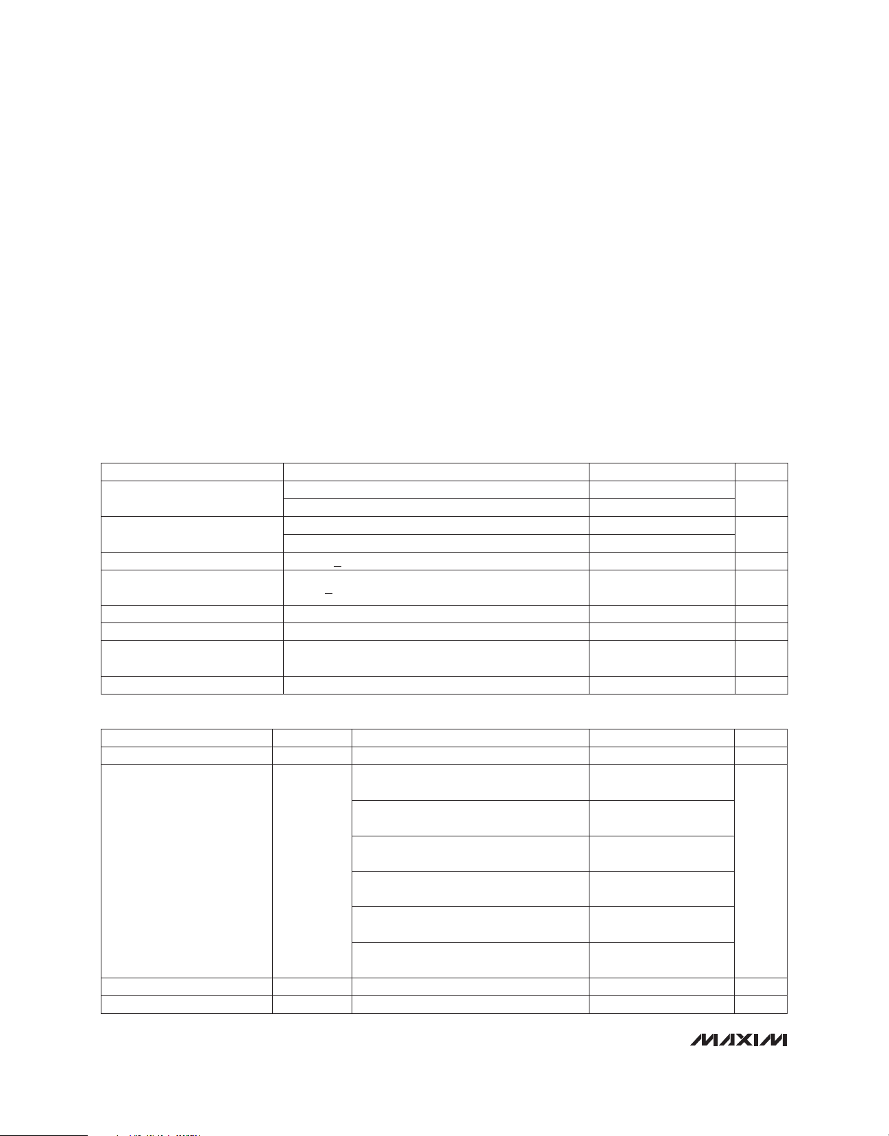
SPECIFICATION TABLES
(Typical values measured at VCC = 3.3V, TA = +25NC, unless otherwise specified.)
OPERATING CONDITIONS
PARAMETER CONDITIONS MIN TYP MAX UNITS
Supply Voltage
(Note 1)
Operating Ambient
Temperature
Supply Noise Tolerance 100kHz < f < 200MHz 50 mV
AC Common-Mode Noise at the
Input
Bit Rate NRZ data (Note 2) 8.5 Gbps
CID Consecutive identical digits (bits) 100 Bits
Time to Reach 50% Mark/Space
Ratio
DC-Blocking Capacitor For bursty traffic such as SAS/SATA 12 nF
2.5V supply 2.375 2.5 2.625
3.3V supply 2.97 3.3 3.63
2.5V supply 0 +25 +85
3.3V supply -40 +25 +85
2MHz < f < 200MHz 150 mV
For continuous traffic 1
Continuous Power Dissipation (TA = +70NC)
48-Pin TQFN (derate 27.8mW/NC above +70NC) ............2.22W
Storage Ambient Temperature Range ............. -65NC to +150NC
ESD Human Body Model, Any Pin ................................. Q2000V
Lead Temperature (soldering, 10s) ................................+300NC
Soldering Temperature (reflow) ......................................+260NC
V
NC
P-P
P-P
Fs
SUPPLY CHARACTERISTICS: 2.5V
PARAMETER SYMBOL CONDITIONS MIN TYP MAX UNITS
Supply Voltage V
Supply Current I
Inrush Current
Power-On Delay t
2 ______________________________________________________________________________________
CC
CC
DI
CC
POWERON
Four outputs in level 3 drive; squelch
turned on
Four outputs in level 3 drive; squelch
turned off
Four outputs in level 2 drive; squelch
turned on
Four outputs in level 2 drive; squelch
turned off
Four outputs in level 1 drive; squelch
turned on
Four outputs in level 1 drive; squelch
turned off
(Note 3) +10 %
(Note 3) 100 ms
-5% 2.5 +5% V
320 385
306 365
286 340
271 325
235 280
221 265
mA
Page 3
8.5Gbps Quad Equalizer and
Preemphasis Drive
SUPPLY CHARACTERISTICS: 3.3V
PARAMETER SYMBOL CONDITIONS MIN TYP MAX UNITS
Supply Voltage V
Supply Current I
Inrush Current
Power-On Delay t
CC
CC
DI
CC
POWERON
Four outputs in level 3 drive; squelch
turned on
Four outputs in level 3 drive; squelch
turned off
Four outputs in level 2 drive; squelch
turned on
Four outputs in level 2 drive; squelch
turned off
Four outputs in level 1 drive; squelch
turned on
Four outputs in level 1 drive; squelch
turned off
(Note 3) +10 %
(Note 3) 100 ms
LVCMOS INPUT
(ADDR[4:1], I2C_EN, SDSF, SQ, OC_EN, TX_EN, TX_LV0, TX_LV1, TX_PE0, TX_PE1, RESET, TEST.)
PARAMETER SYMBOL CONDITIONS MIN TYP MAX UNITS
Input-Voltage High V
Input-Voltage Low V
Input Current I
IH, IIL
IH
IL
VCC = 2.5V ±5%, 3.3V ±10%
VCC = 2.5V ±5%, 3.3V ±10% -0.3
VIN = VCC or GND -200 +200
-10% 3.3 +10% V
0.7 x
V
CC
370 445
354 430
334 405
318 390
272 330
257 315
VCC +
0.3
0.3 x
V
CC
MAX3987
mA
V
V
FA
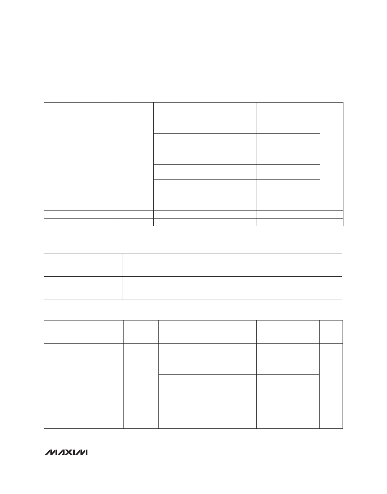
HIGH-SPEED INPUTS
PARAMETER SYMBOL CONDITIONS MIN TYP MAX UNITS
Propagation Delay from Any
Input to Any Output
Output Channel-to-Channel
Delay Skew
Input Sensitivity at the Device
Pin (Note 5)
Residual Deterministic Jitter:
6.5Gbps (Notes 6, 7, 9)
_______________________________________________________________________________________ 3
t
PD
t
SKEW
V
SENSITIVITY
(Point B in
Figure 2)
DJ
RX
Output at level 3 250 ps
Output at level 3 (Note 4) 20 40 ps
Offset cancellation off 75
mV
Offset cancellation on 50
Less than 2in FR4 at the output; max
reach 24in FR4; Maxim stress pattern
(Note 8)
Less than 2in FR4 at the output; max
reach 30in FR4; PRBS7 pattern
0.1 0.2
UI
0.07
P-P
Page 4
8.5Gbps Quad Equalizer and
Preemphasis Drive
HIGH-SPEED INPUTS (continued)
PARAMETER SYMBOL CONDITIONS MIN TYP MAX UNITS
Less than 2in FR4 at the output; max
Residual Deterministic Jitter:
7.5Gbps (Notes 6, 7, 9)
MAX3987
Residual Deterministic Jitter:
8.5Gbps (Notes 6, 7, 9)
DJ
DJ
RX
RX
reach 24in FR4; Maxim stress pattern
(Note 8)
Less than 2in FR4 at the output; max
reach 24in FR4; PRBS7 pattern
Less than 2in FR4 at the output; max
reach 20in FR4; Maxim stress pattern
(Note 8)
Less than 2in FR4 at the output; max
reach 20in FR4; PRBS7 pattern
0.12 0.26
UI
0.07
0.10 0.22
UI
0.1
Squelch-Deassert Voltage for
Slow Response Signal Detect
(Notes 8 to 11)
Squelch-Deassert Voltage for
Fast Response Signal Detect
(Notes 9, 11, 12, 13)
Squelch-Assert Voltage for Slow
Response Signal Detect
(Notes 8 to 11)
Squelch-Assert Voltage for Fast
Response Signal Detect
(Notes 9, 11, 12)
Signal Detect and Squelch
Delay (Note 14)
Voltage Input Swing Launched
Differentially at the Source
(Point A in Figure 2 before the
signal encountering any loss)
Input Resistance R
Differential Input Return Loss SDD11 TQFN, 100MHz to 4.25GHz 17 dB
V
SQ_DEAS_S
V
SQ_DEAS_F
V
SQ_AS_S
V
SQ_AS_F
t
SD_SQ
V
LAUNCH
IN
SDL = 0 120
SDL = 1 (default state) 170
SDL = 0 155
SDL = 1 (default state) 220
SDL = 0 50
SDL = 1 (default state) 100
SDL = 0 65
SDL = 1 (default state) 120
Slow-signal detect and squelch is
enabled (Note 8)
Fast-signal detect and squelch is
enabled (Note 12)
Offset cancellation off 400 1800
Offset cancellation on 200 1800
Between signal and V
CC
200
2.5 5.4
50
mV
mV
mV
mV
ns
mV
I
P-P
P-P
P-P
P-P
P-P
4 ______________________________________________________________________________________
Page 5

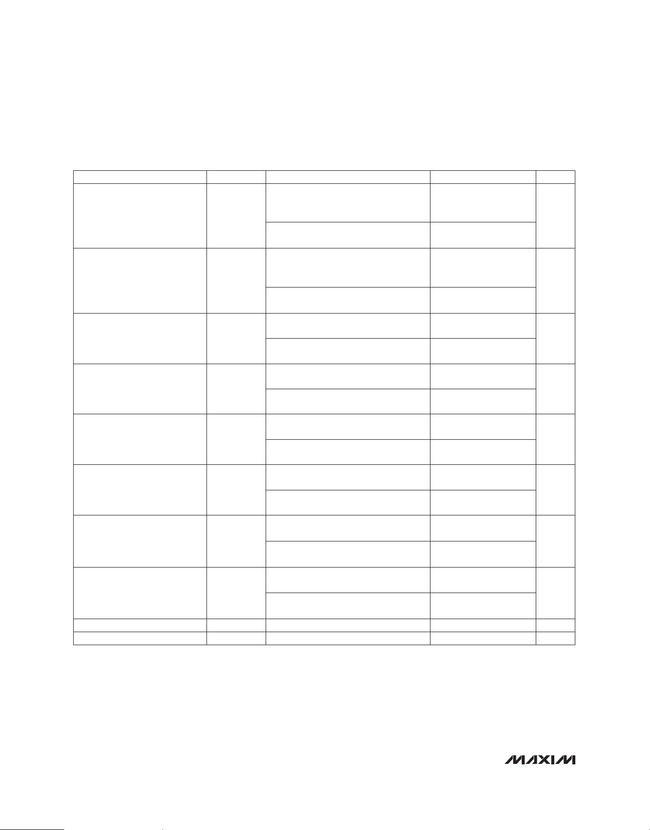
HIGH-SPEED OUTPUTS
PARAMETER SYMBOL CONDITIONS MIN TYP MAX UNITS
Residual Deterministic Jitter:
6.5Gbps
(Notes 6, 8, 9, 15, 16, 17)
Residual Deterministic Jitter:
7.5Gbps
(Notes 6, 8, 9, 15, 16, 17)
Residual Deterministic Jitter:
8.5Gbps
(Notes 6, 8, 9, 15, 16, 17)
Serial-Data Output Rise and
Fall Time
Differential Output Swing:
Level 1 Drive
Differential Output Swing:
Level 2 Drive
Differential Output Swing:
Level 3 Drive
Differential Output Swing:
Level 1 Drive
Differential Output Swing:
Level 2 Drive
Differential Output Swing:
Level 3 Drive
Differential Output Swing:
AC Output Disabled
AC Common-Mode Voltage
Change
DC Common-Mode Voltage
Change
DJ
DJ
DJ
tR/t
V
AC_OUT
V
AC_OUT
V
AC_OUT
V
AC_OUT
V
AC_OUT
V
AC_OUT
V
AC_OUT
V
AC_COM
V
DC_COM
TX
TX
TX
8.5Gbps Quad Equalizer and
Preemphasis Drive
MAX3987
PE = 00, up to 2in FR4; PE = 01, up to
10in FR4; PE = 10, up to 18in FR4;
PE = 11, up to 30in FR4; Maxim stress
pattern
PE = 00, up to 2in FR4; PE = 01, up to
10in FR4; PE = 10, up to 18in FR4;
PE = 11, up to 30in FR4; PRBS7 pattern
PE = 00, up to 2in FR4; PE = 01, up to
10in FR4; PE = 10, up to 16in FR4;
PE = 11, up to 24in FR4; Maxim stress
pattern
PE = 00, up to 2in FR4; PE = 01, up to
10in FR4; PE = 10, up to 16in FR4;
PE = 11, up to 24in FR4; PRBS7 pattern
PE = 00, up to 2in FR4; PE = 01, up to
10in FR4; PE = 10, up to 18in FR4; PE =
11, up to 24in FR4; Maxim stress pattern
PE = 00, up to 2in FR4; PE = 01, up to
10in FR4; PE = 10, up to 18in FR4; PE =
11, up to 24in FR4; PRBS7 pattern
F
20% to 80% of settled value; level 3
drive (Note 4)
When output is enabled; PE = 00;
VCC = 2.5V Q5% (Notes 4, 10)
When output is enabled; PE = 00;
VCC = 2.5V Q5% (Notes 4, 10)
When output is enabled; PE = 00;
VCC = 2.5V Q5% (Notes 4, 10)
When output is enabled; PE = 00;
VCC = 3.3V Q10% (Notes 4, 10)
When output is enabled; PE = 00;
VCC = 3.3V Q10% (Notes 4, 10)
When output is enabled; PE = 00;
VCC = 3.3V Q10% (Notes 4, 10)
When output is powered down; input at
7.5Gbps with D24.3 pattern
(Note 18) 40 mV
(Note 19) -25 +25 mV
30 50 ps
530 600 660 mV
740 840 930 mV
900 1000 1150 mV
530 630 730 mV
750 900 1050 mV
900 1100 1250 mV
0.15 0.20
0.09
0.15 0.23
0.12
0.10 0.15
0.06
50 mV
UI
UI
UI
P-P
P-P
P-P
P-P
P-P
P-P
P-P
P-P
P-P
_______________________________________________________________________________________ 5
Page 6
8.5Gbps Quad Equalizer and
Preemphasis Drive
HIGH-SPEED OUTPUTS (continued)
PARAMETER SYMBOL CONDITIONS MIN TYP MAX UNITS
Average DC Offset Voltage
Change
Output Resistance R
Differential Output Return
Loss
MAX3987
Random Jitter t
Channel Isolation SDD
I2C CHARACTERISTICS
PARAMETER SYMBOL CONDITIONS MIN TYP MAX UNITS
Low-Level Input Voltage V
High-Level Input Voltage V
Low-Level Output Voltage V
SDATA Leakage Current I
Output Fall Time V
V
ILMAX
Input Current Each I/O Pin I
SCLK Clock Frequency f
Note 1: 2.5V covers 0NC to +85NC, and 3.3V covers -40NC to +85NC.
Note 2: With offset cancellation off, the minimum data rate is limited by the DC-blocking capacitor value; with offset cancellation
on, the minimum data rate is limited above 1Gbps.
Note 3: Supply voltage ramp-up time of less than 200Fs. Power-on delay interval measured from the 50% level of the final volt-
age at the device side of filter to 50% of final current. See Figure 1 for a typical supply filter.
Note 4: Guaranteed by design and characterization with a K28.7 pattern at 7.5Gbps, PE = 00.
Note 5: Minimum input amplitude to generate full output swing (PE = 00, squelch disabled). Guaranteed by design and charac-
terization with 1010 clock pattern at 6Gbps. Input sensitivity can be frequency dependent because of the input equalization network. Outputs reach within 90% of settled value at level 3 drive.
Note 6: Difference in deterministic jitter between reference data source and equalizer output. Residual DJ = Output DJ - Source
DJ. The deterministic jitter at the output of the transmission line must be from media-induced loss and not from clock
source modulation.
Note 7: Input signal at point A in Figure 2. No more than 2in FR4 at the output. PE setting = 00, output drive at level 3, offset can-
cellation off. Signal is applied differentially at input to a 6-mil wide, loosely coupled microstrip up to 30in.
Note 8: Maxim stress pattern is 464 bits: PRBS 27, 100 zeros, 1010, PRBS 27, 100 ones, 0101.
Note 9: All four channels are populated with traffic of the same data pattern to the channel under test with outputs set at level 3.
Note 10: Guaranteed by test at 7.5Gbps.
Note 11: Less than 2in FR4 at the input and less than 2in FR4 at the output.
Note 12: Guaranteed at 1.5Gbps and 3Gbps.
Note 13: Tested with ALIGN (0) pattern at 6.0Gbps.
Note 14: For the channel under test, time from the input differential peak-to-peak level rising above the squelch-deassert voltage
(dropping below the squelch-assert voltage) to the output data reaching 90% of maximum differential peak-to-peak level
for input transition from idle to active (10% of maximum differential peak-to-peak level for inputs transition from active to
idle). Squelch of individual output is completed (see Figure 3).
Note 15: No more than 2in FR4 at the input. Output drive is applied differentially to a 6-mil wide, loosely coupled differential
microstrip up to 30in. Output measured at the point C in Figure 4. Input level = 100mV
IHMAX
to
DV
OFFSET
OUT
SD22
LEAKAGE
RJ
ISO
OL1
t
OF
SCL
(Note 20) -25 +25 mV
Between signal and VCC 50
100MHz to 4.25GHz; output on; PE = 11,
LV = 10
(Note 21) 1 ps
Up to 5GHz (Note 22) 38 dB
IL
IH
At IOL = 3mA sink current 0 0.4
IOL = 6mA 0 0.6
I2C output high 0 10
I
0.1VCC < VI < 0.9V
CC
-0.5
0.7 x
V
CC
60 250 ns
-10 +10
P-P
17 dB
.
0.3 x
V
CC
VCC +
0.5
400 kHz
P-P
I
RMS
V
V
V
FA
FA
6 ______________________________________________________________________________________
Page 7
8.5Gbps Quad Equalizer and
Preemphasis Drive
Note 16: The output PE level is defined as the ratio of peak-to-peak voltage of a transition bit to the peak-to-peak voltage of a non-
transition bit.
Note 17: For lowest (level 1) drive, Tx DJ spec must be met for PE = 00 and 01 only.
Note 18: PE = maximum preemphasis, load is 50I ±1% at each side, output is configured for level 3 drive. The pattern is
11001100 (50% edge density) at 7.5Gbps. AC common-mode output is computed as:
V
where:
VP = time-domain voltage measured at true terminal
VN = time-domain voltage measured at complementary terminal
V
Note 19: The maximum difference in the average DC voltage (V
Note 20: The maximum difference in the average differential voltage (DC offset) component between data present and output on,
Note 21: Guaranteed by design and characterization with a K28.7 pattern at 7.5Gbps with 100mV
Note 22: Measured using a vector-network analyzer (VNA). The VNA detects the signal at the output of the victim channel. All
DC_COM
between data present and output on, and data absent and output squelched. PE = lowest preemphasis, load is 50I
±1% at each side, output is configured for level 3 drive.
and data absent and output squelched. PE = lowest preemphasis, load is 50I ±1% at each side, output is configured
for level 3 drive.
level 3 drive, offset cancellation off.
other inputs and outputs are terminated with 50I. The obtained value excludes the forward gain of the victim amplifier.
= DC common-mode voltage (VP + VN)/2
AC_COM
= ((VP + VN)/2 - V
DC_COM
- DC common-mode voltage (VP + VN)/2) component
DC_COM
)
input swing. Output set at
P-P
MAX3987
3.3V/2.5V
SUPPLY
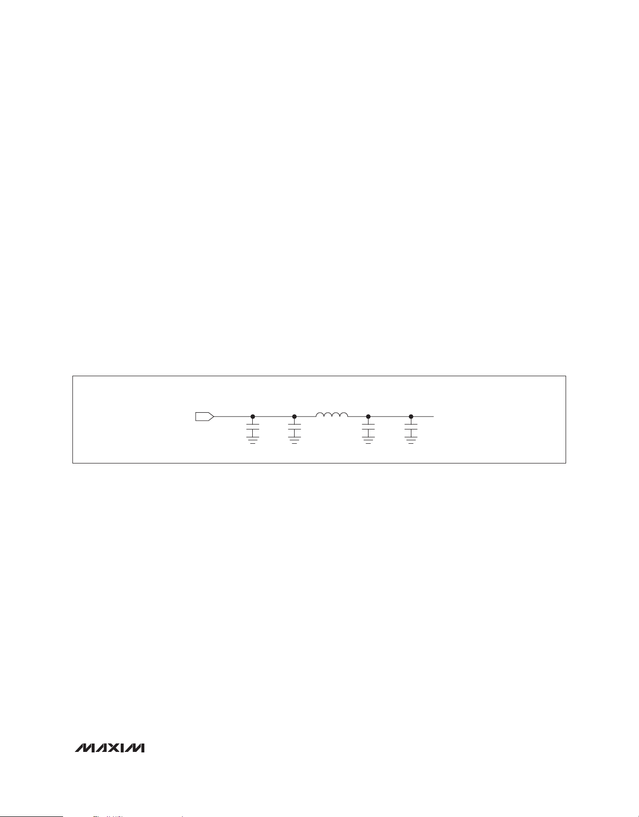
Figure 1. Recommended Supply Filtering
100µF
1µF
0.1µF 100µF 0.1µF
V
CC
_______________________________________________________________________________________ 7
Page 8

8.5Gbps Quad Equalizer and
01
01
01
01
03
Preemphasis Drive
Typical Operating Characteristics
(VCC = +3.3V, TA = +25NC, unless otherwise noted.)
LOSS MEASUREMENT OF TRACE BOARDS
(INPUT POWER OF 0dBm)
0
MAX3987
-10
-20
GAIN (dB)
-30
-40
30in
FREQUENCY (GHz)
0
-10
-20
18in
MAX3987 toc01
24in
987654321
0
INPUT RETURN GAIN (SDD22)
(INPUT POWER OF -40dBm)
POWER-SUPPLY CURRENT
vs. TEMPERATURE (V
400
PREEMPHASIS 11dB
LEVEL 3 OUTPUT
300
PREEMPHASIS 0dB
POWER-SUPPLY CURRENT (mA)
200
LEVEL 1 OUTPUT
-40
TEMPERATURE (°C)
MAX3987 toc04
= 3.3V)
CC
MAX3987 toc02
80600 20 40-20
0
-10
-20
-30
INPUT REFLECTION COEFICIENT (dB)
-40
INPUT CHANNEL-TO-CHANNEL ISOLATION
(INPUT POWER OF 0dBm, PART ENABLED)
-10
-20
-30
-40
GAIN (dB)
-50
CHANNEL RX1 TO RX0
INPUT RETURN GAIN (SDD11)
(INPUT POWER OF -40dBm)
8642
FREQUENCY (GHz)
MAX3987 toc05
MAX3987 toc03
0
-30
INPUT REFLECTION COEFICIENT (dB)
-40
FREQUENCY (MHz)
8642
0
-60
-70
-80
108642
FREQUENCY (GHz)
DETERMINISTIC JITTER vs. LENGTH
TRANSIENT RESPONSE
(3.125Gbps 1010 PATTERN, LV = 10)
0.6
-0.1
-0.2
-0.3
-0.4
-0.5
-0.6
0.5
0.4
0.3
0.2
0.1
0
0
A = 0.5dB, PE = 00
B = 3.2dB, PE = 01
C = 6.6dB, PE = 10
D = 10.5dB, PE = 11
A
B
C
D
200ps/div
MAX3987 toc06
160,000
= 200mV
(V
IN
P-P
DATA RATE = 1.25Gbps)
0.2
0.1
DETERMINISTIC JITTER (UI)
0
FR4 BOARD LENGTH (in)
, MAXIM STRESS PATTERN,
PE = 11
PE = 00
PE = 01
PE = 10
252015105
8 ______________________________________________________________________________________
2
MAX3987 toc07
0
Page 9

8.5Gbps Quad Equalizer and
03
03
03
03
03
03
03
Preemphasis Drive
Typical Operating Characteristics (continued)
(VCC = +3.3V, TA = +25NC, unless otherwise noted.)
DETERMINISTIC JITTER vs. LENGTH
(V
IN
= 200mV
, MAXIM STRESS PATTERN,
P-P
DATA RATE = 3.25Gbps)
DETERMINISTIC JITTER vs. LENGTH
(VIN = 200mV
, MAXIM STRESS PATTERN,
P-P
DATA RATE = 6.25Gbps)
1.0
DETERMINISTIC JITTER vs. LENGTH
(VIN = 200mV
, MAXIM STRESS PATTERN,
P-P
DATA RATE = 7.5Gbps)
1.0
MAX3987
0.4
0.2
DETERMINISTIC JITTER (UI)
PE = 10
0
FR4 BOARD LENGTH (in)
(V
1.0
0.8
0.6
0.4
DETERMINISTIC JITTER (UI)
0.2
0
1000
)
800
P-P
600
400
VERTICAL EYE OPENING (mV
200
0
MAX3987 toc08
0.8
0.6
0.4
DETERMINISTIC JITTER (UI)
0.2
0
PE = 11
PE = 00
PE = 01
252015105
0
DETERMINISTIC JITTER vs. LENGTH
= 200mV
IN
, MAXIM STRESS PATTERN,
P-P
DATA RATE = 8.5Gbps)
PE = 00
PE = 01
15 20 25105
FR4 BOARD LENGTH (in)
PE = 11
PE = 10
0
VERTICAL EYE OPENING vs. LENGTH
(V
IN
= 200mV
, FR4 BOARD, MAXIM
P-P
STRESS PATTERN, DATA RATE = 3.25Gbps)
PE = 00
PE = 01
PE = 10
PE = 11
252015105
0
FR4 BOARD LENGTH (in)
PE = 10
FR4 BOARD LENGTH (in)
MAX3987 toc11
MAX3987 toc13
PE = 11
PE = 00
PE = 01
1000
)
800
P-P
600
400
VERTICAL EYE OPENING (mV
200
600
)
P-P
400
200
VERTICAL EYE OPENING (mV
MAX3987 toc09
0.8
PE = 01
0.6
0.4
DETERMINISTIC JITTER (UI)
0.2
252015105
0
0
PE = 10
PE = 11
FR4 BOARD LENGTH (in)
VERTICAL EYE OPENING vs. LENGTH
(VIN = 200mV
, FR4 BOARD, MAXIM
P-P
STRESS PATTERN, DATA RATE = 1.25Gbps)
PE = 00
PE = 01
PE = 10
PE = 11
0
FR4 BOARD LENGTH (in)
252015105
VERTICAL EYE OPENING vs. LENGTH
(V
IN
= 200mV
, FR4 BOARD,
P-P
STRESS PATTERN, DATA RATE = 6.25Gbps)
PE = 01
PE = 10
PE = 00
0
FR4 BOARD LENGTH (in)
PE = 11
252015105
PE = 00
0
0
MAX3987 toc12
MAX3987 toc14
MAX3987 toc10
252015105
0
_______________________________________________________________________________________ 9
Page 10

8.5Gbps Quad Equalizer and
FR4 BOARD LENGTH (in)
03
FR4 BOARD LENGTH (in)
03
Preemphasis Drive
Typical Operating Characteristics (continued)
(VCC = +3.3V, TA = +25NC, unless otherwise noted.)
VERTICAL EYE OPENING vs. LENGTH
(VIN = 200mV
, FR4 BOARD,
P-P
STRESS PATTERN, DATA RATE = 7.5Gbps)
600
)
MAX3987
P-P
PE = 01
PE = 00
PE = 10
PE = 11
252015105
400
200
VERTICAL EYE OPENING (mV
0
OUTPUT OF 30in FR4 DRIVEN BY MAX3987
(LV = 10, PE = 11, 6.25Gbps MAXIM STRESS PATTERN)
40mV/div
MAX3987 toc18
)
MAX3987 toc15
P-P
DETERMINISTIC JITTER (ps
0
VERTICAL EYE OPENING vs. LENGTH
(VIN = 200mV
, FR4 BOARD,
P-P
STRESS PATTERN, DATA RATE = 8.5Gbps)
600
400
200
0
PE = 10
PE = 11
PE = 01
PE = 00
252015105
OUTPUT OF 30in FR4 WITHOUT PREEMPHASIS
(7.5Gbps MAXIM STRESS PATTERN)
40mV/div
MAX3987 toc19
OUTPUT OF 30in FR4 WITHOUT PREEMPHASIS
MAX3987 toc16
0
(6.25Gbps MAXIM STRESS PATTERN)
40mV/div
30ps/div
MAX3987 toc17
OUTPUT OF 30in FR4 DRIVEN BY MAX3987
(LV = 10, PE = 11, 7.5Gbps MAXIM STRESS PATTERN)
40mV/div
MAX3987 toc20
30ps/div
OUTPUT OF 30in FR4 WITHOUT PREEMPHASIS
(8.5Gbps MAXIM STRESS PATTERN)
40mV/div
30ps/div
MAX3987 toc21
10 _____________________________________________________________________________________
30ps/div
OUTPUT OF 30in FR4 DRIVEN BY MAX3987
(LV = 10, PE = 11, 8.5Gbps MAXIM STRESS PATTERN)
40mV/div
30ps/div
MAX3987 toc22
30ps/div
Page 11

8.5Gbps Quad Equalizer and
03
03
Preemphasis Drive
Typical Operating Characteristics (continued)
(VCC = +3.3V, TA = +25NC, unless otherwise noted.)
MAX3987
RECEIVER DETERMINISTIC JITTER vs. LENGTH
(INPUT SIGNAL = 400mV
MAXIM STRESS PATTERN, T
1.0
0.9
0.8
0.7
0.6
0.5
0.4
0.3
DETERMINISTIC JITTER (UI)
8.5Gbps
0.2
0.1
0
FR4 BOARD LENGTH (in)
10.3Gbps
,
P-P
= +27°C)
A
7.5Gbps
6.6Gbps
252015105
RECEIVER DETERMINISTIC JITTER
vs. TEMPERATURE (INPUT SIGNAL = 400mV
PRBS7, 3.125Gbps)
0.5
0.4
0.3
0.2
DETERMINISTIC JITTER (UI)
0.1
0
-40
TEMPERATURE (°C)
18in
16in
20in
30in
24in
806040200-20
RECEIVER DETERMINISTIC JITTER
vs. TEMPERATURE (V
= 400mV
IN
P-P
MAXIM STRESS PATTERN, 7.5Gbps)
0.5
,
MAX3987 toc23
DETERMINISTIC JITTER (UI)
0
,
P-P
MAX3987 toc26
DETERMINISTIC JITTER (UI)
RECEIVER DETERMINISTIC JITTER vs. LENGTH
(INPUT SIGNAL = 400mV
1.0
0.9
0.8
0.7
0.6
0.5
0.4
0.3
6.6Gbps
0.2
0.1
0
FR4 BOARD LENGTH (in)
, PRBS7, TA = +27°C)
P-P
8.5Gbps
7.5Gbps
10.3Gbps
252015105
0
RECEIVER DETERMINISTIC JITTER
vs. TEMPERATURE (INPUT SIGNAL = 400mV
STRESS PATTERN, 6.6Gbps)
0.5
0.4
0.3
20in
0.2
0.1
0
-40
16in
18in
TEMPERATURE (°C)
24in
806040200-20
RECEIVER DETERMINISTIC JITTER
vs. TEMPERATURE (INPUT SIGNAL = 400mV
PRBS7, 7.5Gbps)
0.5
vs. TEMPERATURE (INPUT SIGNAL = 400mV
0.5
MAX3987 toc24
0.4
0.3
0.2
DETERMINISTIC JITTER (UI)
0.1
0
,
vs. TEMPERATURE (INPUT SIGNAL = 400mV
P-P
0.5
MAX3987 toc27
0.4
0.3
0.2
DETERMINISTIC JITTER (UI)
0.1
0
,
P-P
0.5
RECEIVER DETERMINISTIC JITTER
MAXIM STRESS PATTERN, 3.125Gbps)
30in
24in
-40
18in
16in
20in
TEMPERATURE (°C)
RECEIVER DETERMINISTIC JITTER
PRBS7, 6.6Gbps)
30in
24in
20in
-40
18in
16in
TEMPERATURE (°C)
RECEIVER DETERMINISTIC JITTER
vs. TEMPERATURE (V
= 400mV
IN
STRESS PATTERN, 8.5Gbps)
P-P
,
P-P
MAX3987 toc25
806040200-20
,
P-P
MAX3987 toc28
806040200-20
,
0.4
0.3
0.2
DETERMINISTIC JITTER (UI)
0.1
0
-40
TEMPERATURE (°C)
18in
MAX3987 toc29
24in
20in
16in
806040200-20
0.4
0.3
0.2
DETERMINISTIC JITTER (UI)
0.1
0
-40
______________________________________________________________________________________ 11
16in
18in
TEMPERATURE (°C)
20in
24in
30in
MAX3987 toc30
0.4
0.3
16in
0.2
DETERMINISTIC JITTER (UI)
0.1
18in
806040200-20
0
-40
TEMPERATURE (°C)
20in
MAX3987 toc31
806040200-20
Page 12

8.5Gbps Quad Equalizer and
Preemphasis Drive
Typical Operating Characteristics (continued)
(VCC = +3.3V, TA = +25NC, unless otherwise noted.)
RECEIVER DETERMINISTIC JITTER
vs. TEMPERATURE (INPUT SIGNAL = 400mV
PRBS7, 8.5Gbps)
0.5
MAX3987
0.4
0.3
0.2
DETERMINISTIC JITTER (UI)
0.1
0
-40
16in
TEMPERATURE (°C)
20in INPUT FR4, 8.5Gbps, MAXIM STRESS
PATTERN, PE = 00, LV = 00
100mV/div
RECEIVER DETERMINISTIC JITTER
,
vs. TEMPERATURE (INPUT SIGNAL = 400mV
P-P
P-P
,
MAXIM STRESS PATTERN, 10.3Gbps)
0.5
MAX3987 toc32
0.4
30in
20in24in
18in
806040200-20
0.3
0.2
DETERMINISTIC JITTER (UI)
0.1
0
-40
16in
TEMPERATURE (°C)
20in
18in
MAX3987 toc33
806040200-20
24in INPUT FR4, 6Gbps, MAXIM STRESS
MAX3987 toc35
PATTERN, PE = 00, LV = 00
100mV/div
MAX3987 toc36
RECEIVER DETERMINISTIC JITTER
vs. TEMPERATURE
(V
= 400mV
IN
0.5
0.4
0.3
18in
0.2
DETERMINISTIC JITTER (UI)
0.1
20in
0
-40
, PRBS7, 10.3Gbps)
P-P
16in
TEMPERATURE (°C)
24in
24in INPUT FR4, 7.5Gbps, MAXIM STRESS
PATTERN, PE = 00, LV = 00
100mV/div
MAX3987 toc34
806040200-20
MAX3987 toc37
24ps/div
30ps/div
BER MEASUREMENT (BER < 1e-12)
24in INPUT FR4, 10.3Gbps, PRBS7 PATTERN,
PE = 00, LV = 00
100mV/div
22ps/div
MAX3987 toc38
30in INPUT FR4, 7.5Gbps, PRBS7 PATTERN,
PE = 00, LV = 00
100mV/div
22ps/div
MAX3987 toc39
18in INPUT AND OUTPUT FR4, INPUT
SIGNAL: 400mV
P-P
12 _____________________________________________________________________________________
24ps/div
, 7.5Gbps, PRBS31
MAX3987 toc40
Page 13

8.5Gbps Quad Equalizer and
Preemphasis Drive
Pin Configuration
TOP VIEW
V
CC
SDSF
SQ
OC_EN
TX_EN
SDATA
SCLK
GND
TX_LV0
TX_LV1
V
CC
V
CC
*EXPOSED PAD.
RX3+
RX2-
GND
RX3-
35
34 33 32 31 30 29 28 27
36
37
38
39
40
41
42
GND
TX2-
MAX3987
CC
V
TX2+
43
44
45
46
47
+
48
2
3456 78910
1
TX3-
TX3+
RX1+
RX1-
VCCVCCRX2+
CC
V
TX1-
TX1+
EP*
GND
GND
RX0+
RX0-
25
26
24
V
CC
23
ADDR1
22
ADDR2
21
ADDR3
20
ADDR4
19
TEST
18
N.C.
17
RESET
16
TX_PE0
15
TX_PE1
14
I2C_EN
13
V
CC
12
11
TX0-
TX0+
MAX3987
Pin Description
PIN NAME FUNCTION
1 TX3- Negative CML Output Signal
2 TX3+ Positive CML Output Signal
3, 10, 27, 34, 44 GND Negative Power Supply (Ground)
4 TX2- Negative CML Output Signal
5 TX2+ Positive CML Output Signal
6, 7, 13, 24, 30,
31, 37, 47, 48
8 TX1- Negative CML Output Signal
9 TX1+ Positive CML Output Signal
11 TX0- Negative CML Output Signal
12 TX0+ Positive CML Output Signal
14 I2C_EN LVCMOS Signal to Enable/Disable I2C Programming Interface
15 TX_PE1 LVCMOS Signal to Set Output Preemphasis Levels
16 TX_PE0 LVCMOS Signal to Set Output Preemphasis Levels
17 RESET LVCMOS Signal to Reset the Device to Default Configuration When High
18 N.C. No Connection. Leave this pin unconnected.
______________________________________________________________________________________ 13
V
CC
Positive Power Supply. All pins should be set at 3.3V or 2.5V.
Page 14

8.5Gbps Quad Equalizer and
Preemphasis Drive
Pin Description (continued)
PIN NAME FUNCTION
19 TEST Reserved for Manufacturing Test. Connect to ground.
20–23 ADDR[4:1] LVCMOS Signal for I2C Serial Interface Address
25 RX0+ Positive CML Differential Data Input Signal
26 RX0- Negative CML Differential Data Input Signal
MAX3987
28 RX1+ Positive CML Differential Data Input Signal
29 RX1- Negative CML Differential Data Input Signal
32 RX2+ Positive CML Differential Data Input Signal
33 RX2- Negative CML Differential Data Input Signal
35 RX3+ Positive CML Differential Data Input Signal
36 RX3- Negative CML Differential Data Input Signal
38 SDSF LVCMOS Signal to Select Signal Detect Type
39 SQ LVCMOS Signal to Enable/Disable Output Squelch and Signal Detect
40 OC_EN LVCMOS Signal to Enable/Disable Offset Cancellation
41 TX_EN LVCMOS Signal to Power On/Off Transmitter
42 SDATA Analog I2C Serial Interface Data Input and Output
43 SCLK Analog I2C Serial Interface Clock Input
45 TX_LV0 LVCMOS Signal to Set Output Amplitude
46 TX_LV1 LVCMOS Signal to Set Output Amplitude
— EP
Exposed Pad. Signal and supply common. For optimal thermal conductivity and supply return (GND), this pad must be soldered to circuit board ground.
Detailed Description
The MAX3987 is a 4-channel equalizer and preemphasis driver that accepts CML differential signals whose
data rates vary from 1Gbps to 8.5Gbps. Each channel
has a fixed equalization network and programmable
preemphasis driver. All controls for preemphasis, output swing level, signal detect/squelch, offset cancellation, output enable/disable, output polarity, etc., are
programmed through the I2C interface. These functions
are implemented through a programming block on-chip
where control bits can be received through a serial bus
or through control pins at the edge of the chip. A block
diagram is shown in Figure 5.
14 _____________________________________________________________________________________
The MAX3987 has a built-in power-on reset function.
After the power-on reset, or when RESET is asserted, all
4 channels are configured to a “default” state. Table 1
describes the functions that are controlled and the default
state on reset if all the control pins are not connected.
Global and Individual
Channel Programming
The MAX3987 supports global programming through
hardware pins (only applicable to EQ/PE) and individual
channel programming through I2C. Table 1 describes
the control pins and their function.
Power-On Reset
Page 15

8.5Gbps Quad Equalizer and
Preemphasis Drive
Table 1. Function Table
PIN NAME
I2C_EN 0
SDSF 0 See Table 2.
SQ 1 See Table 2.
OC_EN 0 Offset cancellation turned off. Offset cancellation turned on.
TX_EN 1 All outputs powered off. All outputs powered on.
TX_LV0 0
TX_LV1 1
TX_PE0 1
TX_PE1 0
SDATA, SCLK — See the Device Power-Up and Reset and I2C Programming section.
RESET 0
ADDR4 0 I2C address bit = 0 I2C address bit = 1
ADDR3 0 I2C address bit = 0 I2C address bit = 1
ADDR2 0 I2C address bit = 0 I2C address bit = 1
ADDR1 0 I2C address bit = 0 I2C address bit = 1
*Default is set by internal pullup or pulldown resistors of 40kI.
INTERNAL
DEFAULT*
PIN VALUE, X = 0 PIN VALUE, X = 1
Selects the pin configuration mode
(TX_EN, TX_LV0, TX_LV1, TX_PE0,
TX_PE1, SDSF, SQ, OC_EN). In this
mode, I2C read of pin settings is
supported.
See Table 4.
Global output preemphasis control. See Table 3.
The device is in normal operation
mode.
Selects the I2C serial interface for
programming. Registers can be read and
write for full configuration.
The device is reset. After releasing reset (upon
the falling edge of RESET), the MAX3987
acquires a startup configuration depending
on whether it is an EQ/PE or a crosspoint,
independent of the I2C_EN signal status.
MAX3987
Software Power-Down of Individual Output
With the software power-down feature, unused outputs
can be turned off by programming a hardware pin or
through I2C. It is recommended that any change in programming that affects power be executed only as part of
an initialization sequence.
Signal Detect and Internal Squelch
Signal detect and internal squelch suit several applications like Fibre Channel, PCIe, and SAS/SATA.
Signal detect can be enabled and disabled for each
individual input by sensing the presence of a valid input
signal. Signal detect controls the squelch of the corresponding output (see Table 2).
Squelch can be enabled and disabled independently
for each individual output that is controlled by a specific
input. The output power-down overrides squelch. When
an output is squelched, both terminals of the differential
______________________________________________________________________________________ 15
Table 2. Signal Detect and Squelch Pin
Programming
PIN
VALUE
SDSF = 0 Select slow-response signal detect (SD1).
SDSF = 1 Select fast-response signal detect (SD2).
SQ = 0 Signal detect and output squelch disabled.
SQ = 1 Signal detect and output squelch enabled.
output are set to the common-mode DC voltage (differential zero voltage).
Signal detect and internal squelch have one setting for
fast-response applications such as SAS/SATA and PCIe,
and another setting for slow-response applications such
as XAUI, Fibre Channel, and InfiniBand cable applications. They are controllable through the I2C serial programming interface or hardware pin.
SIGNAL DETECT AND SQUELCH
SELECTION
Page 16

8.5Gbps Quad Equalizer and
Preemphasis Drive
Signal-detect status of each input can be monitored
through the I2C interface.
Signal detect assert/deassert has two programmable
levels for each individual channel. They are accessible
only through the I2C interface. The default threshold
level for signal detect is high.
Input Equalization
MAX3987
One fixed, universal input equalization level of approximately 15dB compensates any length up to 30in, 6-milwide FR4 microstrip up to 8.5Gbps. The device can also
compensate up to 8m to 10m 24 AWG twin axial cable.
Input Offset Cancellation
Each input path has an option to enable and disable
offset cancellation for high-sensitivity applications. It is
SIGNAL
SOURCE
A B
4TH OBT
LPF
SMA
CONNECTOR
MICROSTRIP
2in < L < 30in L < 2in
6-MIL
programmable through pin or I2C interface. It typically
requires signal detect and squelch turned off to realize
its full benefits.
When offset cancellation is on, the minimum data rate is
1Gbps. It is suggested that offset cancellation be turned
off for SAS/SATA or PCIe bursty applications.
Output Preemphasis
Four different levels of preemphasis at the driver output are selectable to compensate for driving different
lengths of PCB routing or cables. The PE levels are 0dB,
3dB, 7dB, and 11dB. The PE level can be set either for
all the outputs globally or for each output individually.
See Table 3.
PCB
MAX3987
IN OUT
6-MIL
MICROSTRIP
CONNECTOR
SMA
SCOPE OR
ERROR
DETECTOR
FR4
< 4.4
4.0 < E
R
tanδ = 0.022
Figure 2. Receive Equalizer Test Setup. The points labeled A and B are referenced for AC parameter test conditions. The filter is a
lowpass fourth-order Bessel-Thompson or equivalent (BW = 0.75 x bit rate Q10%).
TIME DELAY FROM INPUT SQUELCH ASSERT TO OUTPUT ENABLED
t
DIFFERENTIAL
INPUT SIGNAL
V
SQ_DEAS_
IDLE BURST
V
SQ_AS_
IN
SD_SQ
90% FULL-SWING
DIFFERENTIAL P-P
OUT
MAX3987
t
SD_SQ
TIME DELAY FROM INPUT SQUELCH ASSERT TO OUTPUT SQUELCHED
DIFFERENTIAL
OUTPUT SIGNAL
10% FULL-SWING
OUTPUT SIGNAL
Figure 3. Input Signal Detect and Output Squelch and Its Timing Definition
16 _____________________________________________________________________________________
Page 17

8.5Gbps Quad Equalizer and
Preemphasis Drive
MAX3987
PCB
SIGNAL
SOURCE
4TH OBT
LPF
Figure 4. Preemphasis Test Setup. The points labeled A and C are referenced for AC parameter test conditions. The filter is a lowpass fourth-order Bessel-Thompson or equivalent (BW = 0.75 x bit rate Q10%).
Output Level
Three different output levels can be programmed for all
outputs. The nominal level 1 output drive is approximately 600mV
is approximately 850mV
when level setting LV = 00. The level 2 drive
P-P
when level setting LV = 01,
P-P
and the level 3 drive is approximately 1050mV
level setting LV = 10. This control can be programmed
globally or individually. See Table 4.
Programming Interface
An I2C serial interface is provided to support global
and individual programming. Hardware pins (TX_EN,
TX_LV0, TX_LV1, TX_PE0, TX_PE1, SDSF, SQ, OC_EN)
A
6-MIL
MICROSTRIP
SMA
CONNECTOR
L < 2in 2in < L < 30in
MAX3987
IN OUT
MICROSTRIP
are also provided to support global programming including output drive level, PE level, signal detect/squelch
selection, outputs on/off, and offset cancellation.
P-P
when
Table 5 details the register map showing the address,
name, and function. The detailed registers are shown in
Tables 6 to 11.
All data input and output connections are AC-coupled
with typical 100nF for continuous traffic, and 12nF maximum for bursty traffic such as SAS/SATA.
6-MIL
CONNECTOR
C
SMA
SCOPE OR
ERROR
DETECTOR
FR4
< 4.4
4.0 < E
R
tanδ = 0.022
Register Maps
Input and Output Coupling
Table 3. PE Pin Programming
PIN VALUE PE PREEMPHASIS VALUE (dB)
TX_PE1 = 0 TX_PE0 = 0 00 0
TX_PE1 = 0 TX_PE0 = 1 01 3
TX_PE1 = 1 TX_PE0 = 0 10 7
TX_PE1 = 1 TX_PE0 = 1 11 11
Table 4. Drive Level Pin Programming
PIN VALUE LV OUTPUT DRIVE LEVEL
TX_LV1 = 0 TX_LV0 = 0 00 Level 1 Drive (minimum)
TX_LV1 = 0 TX_LV0 = 1 01 Level 2 Drive
TX_LV1 = 1 TX_LV0 = 0 10 Level 3 Drive (maximum)
TX_LV1 = 1 TX_LV0 = 1 — Do not use this mode.
______________________________________________________________________________________ 17
Page 18

8.5Gbps Quad Equalizer and
Preemphasis Drive
Table 5. Register Map
ADDRESS NAME REGISTER BITS R/W
1 XPE TX PE 8 R/W
2 XLV TX Level 8 R/W
3 XOP TX ON and Polarity 8 R/W
4 SDM Signal-Detect Mode 8 R/W
MAX3987
Table 6. Register 1: TX PE (XPE)
Bit
Function
Default TXPE1 TXPE0 TXPE1 TXPE0 TXPE1 TXPE0 TXPE1 TXPE0
5 OCS Offset Cancellation and Squelch 8 R/W
6 SDS Signal-Detect Status 8 R
7 6 5 4 3 2 1 0
TX3 PE
SELECT 1
PE SELECT FUNCTION
BIT[1:0] FUNCTION (dB)
00
01
10
11
TX3 PE
SELECT 0
TX2 PE
SELECT 1
≈ 0
≈ 3
≈ 7
≈ 11
TX2 PE
SELECT 0
TX1 PE
SELECT 1
TX1 PE
SELECT 0
TX0 PE
SELECT 1
TX0 PE
SELECT 0
Table 7. Register 2: TX Level (XLV)
Bit
Function
Default TXLV1 TXLV0 TXLV1 TXLV0 TXLV1 TXLV0 TXLV1 TXLV0
BIT[1:0] FUNCTION (mV)
00
01
10
11 Do not use
7 6 5 4 3 2 1 0
TX3 LEVEL
SELECT 1
TX LEVEL SELECT FUNCTION
TX3 LEVEL
SELECT 0
TX2 LEVEL
SELECT 1
≈ 600
≈ 850
≈ 1050
TX2 LEVEL
SELECT 0
TX1 LEVEL
SELECT 1
TX1 LEVEL
SELECT 0
TX0 LEVEL
SELECT 1
TX0 LEVEL
SELECT 0
Table 8. Register 3: TX ON and Polarity (XOP)
Bit
Function TX3 ON TX2 ON TX1 ON TX0 ON TX3 POL TX2 POL TX1 POL TX0 POL
Default TXEN TXEN TXEN TXEN 0 0 0 0
If TXEN is zero, the output signal for that channel is off. If TX[3:0] POL is zero, there is no polarity inversion for that
channel.
7 6 5 4 3 2 1 0
18 _____________________________________________________________________________________
Page 19

8.5Gbps Quad Equalizer and
Preemphasis Drive
Table 9. Register 4: Signal-Detect Mode (SDM)
Bit
Function SQ3 SQ2 SQ1 SQ0 SF3 SF2 SF1 SF0
Default SQ SQ SQ SQ SF SF SF SF
SF function: 0 = slow, 1 = fast. A zero selects slow-response signal detect; a one selects fast signal detect.
SQ function: 0 disables the squelch; 1 enables squelch.
Table 10. Register 5: Offset Cancellation and Squelch (OCS)
Bit
Function OC3 OC2 OC1 OC0 SDL3 SDL2 SDL1 SDL0
Default OCEN OCEN OCEN OCEN 1 1 1 1
If OCEN = 1, offset cancellation is enabled; if OCEN = 0, offset cancellation is off.
If the SDL bit = 0, the signal-detect threshold level is low. If the SDL bit = 1, the signal-detect threshold level is high.
Table 11. Register 6: Signal-Detect Status (SDS)
Bit
Function — — — — SD3 SD2 SD1 SD0
Default — — — — — — — —
If the SD bit = 0, the signal is present in the corresponding channel.
7 6 5 4 3 2 1 0
7 6 5 4 3 2 1 0
7 6 5 4 3 2 1 0
MAX3987
Figure 5. Functional Diagram
TEST
OC_EN
ADDR[4:1]
I2C_EN
SCLK
SDATA
RESET
RX[3:0]+/-
4
SIGNAL
DETECT
V
CC
EQUALIZER AND AMPLIFIER
CORE
CONFIGURATION REGISTER
PROGRAMMING BLOCK
GND
SQUELCH
CONTROL
MAX3987
TX[3:0]+/-
4
TX_EN
SDSF
SQ
TX_LV0
TX_LV1
TX_PE0
TX_PE1
______________________________________________________________________________________ 19
Page 20

8.5Gbps Quad Equalizer and
Preemphasis Drive
Device Power-Up and Reset
and I2C Programming
Power-Up and Reset
Default Condition
The MAX3987 enters the default condition on power-up
or on assertion of the RESET signal. The RESET signal
is active high. When RESET is deasserted, the power-
MAX3987
up sequence disables the MAX3987 for 100ms, during
which the MAX3987 does not respond to the I2C port.
At the end of the 100ms timeout, the MAX3987 samples
the control pins and programs the control registers
according to the register map.
After power-up the MAX3987 listens to the I2C bus and
can be accessed for read or write at any time if the
I2C_EN pin is asserted, or for read access only if the
I2C_EN pin is not asserted.
I2C Control
The MAX3987 can be configured through the control
pins or the I2C interface. When I2C_EN is asserted, the
control pin’s only role is to set the default value of the
control registers during power-on reset. Other than during power-on reset, the control pins do not control the
functionality of the chip. The I2C interface can write and
read the control registers.
When I2C_EN is not asserted, the MAX3987 is in pin
control mode. The control pins affect the functionality of
the chip, and each control pin controls all the channels.
The I2C interface can only read the control registers, and
only channel 0 bits are valid and apply to all channels.
All other bits are zero.
I2C Programming
The MAX3987 I2C function implements only the mandatory fast-mode slave functions. Implemented features
are START condition, STOP condition, acknowledge,
and 7-bit address.
The I2C address comprises a fixed address, which is
100, and 4 bits of programmable address. During the
first I2C cycle the fixed address should match data in
bits [7:5] and the programmable address should match
bits [4:1]. Bit 0 is the I2C R/W bit.
A power-on reset or assertion of the RESET signal, or
an I2C START or STOP condition, always resets the
register address to zero. If I2C_EN is asserted, write
and read access to the registers is enabled. If I2C_EN
is not asserted, only read access is enabled, and the
MAX3987 acknowledges a write cycle, but does not
write into any register.
Each I2C access starts with the address and read/write
byte. The first access always addresses register 0,
which is the XPE register. For each subsequent access,
the MAX3987 autoincrements the register addresses.
The register address does not increment above address
6. If there are more than six consecutive read cycles,
the MAX3987 acknowledges and provides zero data. If
there are more than five consecutive write cycles, the
MAX3987 acknowledges and does not write into any
register.
The MAX3987 internal registers change at the end of the
write cycle, when all 8 bits are written. The control function changes approximately 200ns after the rising edge
of SCLK, which samples the I2C LSB.
XLVXPESTART XOP SDM OCS ... ... STOP100...0
Figure 6. EQ I2C Write Sequence
XLVXPESTART XOP SDM OCS 0...0 0...0 STOP100...1
Figure 7. EQ I2C Read Sequence
20 _____________________________________________________________________________________
Page 21

RX_+
RX_-
35I
35I
85I
32I
8.5Gbps Quad Equalizer and
Preemphasis Drive
MAX3987
V
CC
TRANSIENT
V
CC
TRANSIENT
85I
SUPRESSOR
CLAMP
SUPRESSOR
CLAMP
50I 50I
6.5mA 3mA 2mA
LEVEL
CONTROL
TX_LV[1:0]
TX_+
TX_-
Figure 8. Simplified Input Circuit
Input and Output Buffers
The input buffers and the output drivers are current-mode
logic (CML). The input buffers consist of a 50I load
resistor connected to VCC and the input connected to
a differential equalizer as shown in Figure 8. The output
circuit is shown in Figure 9. The ESD protection for both
the input and output circuitry consists of diodes connected to a transient voltage suppressor clamp shown as
a Schottky diode. For more information about the function
of the suppressor clamp, refer to the Detailed Description
section of the MAX3208E IC data sheet.
Using the MAX3987 in PCIe
Applications
The MAX3987 does not support presence detection.
However, it passes low-frequency beacon signals and
has signal detect and output squelch compatibility with
the electrical idle state requirements.
Figure 9. Standard Output Circuit
Package and Exposed Pad
The exposed-pad, 48-pin thin QFN package incorporates features that provide a very low-thermal resistance
path for heat removal from the IC. The exposed pad
on the MAX3987 must be soldered to the circuit board
for proper thermal performance and correct electrical
grounding. Refer to Application Note 862: HFAN-08.1:
Thermal Considerations of QFN and Other ExposedPaddle Packages for additional information.
Package Information
For the latest package outline information and land patterns (footprints), go to www.maxim-ic.com/packages.
Note that a “+”, “#”, or “-” in the package code indicates
RoHS status only. Package drawings may show a different suffix character, but the drawing pertains to the
package regardless of RoHS status.
PACKAGE
TYPE
48 TQFN-EP T4877+4
PACKAGE
CODE
DOCUMENT
NO.
21-0144 90-0130
LAND
PATTERN
NO.
______________________________________________________________________________________ 21
Page 22

8.5Gbps Quad Equalizer and
Preemphasis Drive
Revision History
REVISION
NUMBER
0 11/09 Initial release —
MAX3987
1 1/10
2 4/12
REVISION
DATE
DESCRIPTION
Corrected the naming convention for SAS, SATA in the Applications and Features
sections
Added the soldering temperature line to the Absolute Maximum Ratings section 2
Added the EP description to the Pin Description table 14
Added the Using the MAX3987 in PCIe Applications section 21
Corrected the storage ambient temperature range in the Absolute Maximum
Ratings section
PAGES
CHANGED
1
2
Maxim cannot assume responsibility for use of any circuitry other than circuitry entirely embodied in a Maxim product. No circuit patent licenses are implied.
Maxim reserves the right to change the circuitry and specifications without notice at any time.
22 Maxim Integrated Products, 120 San Gabriel Drive, Sunnyvale, CA 94086 408-737-7600
©
2012 Maxim Integrated Products Maxim is a registered trademark of Maxim Integrated Products, Inc.
 Loading...