

General Description
The MAX3984 is a single-channel, preemphasis driver
with input equalization that operates from 1Gbps to
10.3Gbps. It provides compensation for copper links,
such as 8.5Gbps Fibre Channel and 10.3Gbps
Ethernet, allowing spans of up to 10m with 24 AWG
cable. The driver provides four selectable preemphasis
levels, and the selectable input equalizer compensates
for up to 10in of FR-4 circuit board material at 10Gbps.
The MAX3984 also features SFP-compliant loss-of-signal (LOS) detection and TX_DISABLE. Selectable output swing reduces EMI and power consumption. The
MAX3984 is packaged in a lead-free, 3mm x 3mm,
16-pin thin QFN and operates from a 0°C to +85°C temperature range.
Applications
Features
♦ Drives Up to 10m of 24 AWG Cable
♦ Drives Up to 30in of FR-4
♦ Selectable 1000mV
P-P
or 1200mV
P-P
Differential
Output Swing
♦ Selectable Output Preemphasis
♦ Selectable Input Equalization
♦ LOS Detection with Built-In Squelch
♦ Transmit Disable
♦ Hot Pluggable
MAX3984
1Gbps to 10Gbps Preemphasis Driver with
Receive Equalizer
________________________________________________________________
Maxim Integrated Products
1
Ordering Information
19-0868; Rev 0; 7/07
For pricing, delivery, and ordering information, please contact Maxim Direct at 1-888-629-4642,
or visit Maxim’s website at www.maxim-ic.com.
+
Denotes a lead-free package.
*EP = Exposed pad.
Pin Configuration appears at end of data sheet.
Typical Operating Circuits continued at end of data sheet.
8.5Gbps Fibre Channel
10.3Gbps Ethernet
Active Cable Assemblies
STM-64
TX_DISABLE
PE1
IN_LEV
PE0
OUT_LEV
IN+
IN-
LOS
V
CC
OR
GND
GND
V
CC
+3.3V
OUT+
OUT-
MAX3984
0.01μF
0.01μF
LOS
PE1
IN_LEV
PE0
OUT_LEV
V
CC
OR
GND
GND
+3.3V
IN+
IN-
MAX3984
OUT+
OUT-
0.01μF
0.01μF
22pF
39Ω
22pF
0.01μF
0.01μF
39Ω
22pF
39Ω
22pF
39Ω
LOS
LOS
PE1
IN_LEV
PE0
OUT_LEV
IN+
IN-
V
CC
OR
GND
GND
+3.3V
OUT+
OUT-
MAX3984
0.01μF
0.01μF
LOS
PE1
IN_LEV
PE0
OUT_LEV
TX_DISABLE
V
CC
OR
GND
GND
V
CC
+3.3V
IN+
IN-
MAX3984
OUT+
OUT-
0.01μF
0.01μF
0.01μF
0.01μF
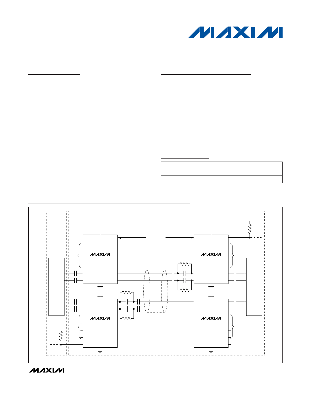
≤ 10m (24 AWG)
UP TO 10Gbps
COPPER CABLE
DIFFERENTIAL
100Ω TWIN-AX
ACTIVE CABLE ASSEMBLY
Tx+
Tx-
Rx+
Rx-
DISK
ENCLOSURE
SWITCH
OR
SERDES
≤ 5V
≥ 4.7kΩ
Rx+
Rx-
Tx+
Tx-
FABRIC SWTCH
SWITCH
OR
SERDES
≤ 5V
R
PULLUP
≥ 4.7kΩ
Typical Operating Circuits
PART
TEMP
RANGE
PIN-PACKAGE
MAX3984UTE+ 0°C to +85°C 16 Thin QFN-EP* T1633F-3
PKG
CODE
MAX3984
1Gbps to 10Gbps Preemphasis Driver with
Receive Equalizer
2 _______________________________________________________________________________________
ABSOLUTE MAXIMUM RATINGS
OPERATING CONDITIONS
Stresses beyond those listed under “Absolute Maximum Ratings” may cause permanent damage to the device. These are stress ratings only, and functional
operation of the device at these or any other conditions beyond those indicated in the operational sections of the specifications is not implied. Exposure to
absolute maximum rating conditions for extended periods may affect device reliability.
Supply Voltage Range (VCC).................................-0.5V to +4.1V
Continuous Output Current Range
(OUT+, OUT-) ...............................................-25mA to +25mA
Input Voltage Range (IN+, IN-) ..................-0.5V to (VCC+ 0.5V)
Logic Inputs Range (PE1, PE0,
TX_DISABLE, IN_LEV, OUT_LEV) ..........-0.5V to (V
CC
+ 0.5V)
LOS Open-Collector Supply Voltage Range
(with ≥ 4.7kΩ pullup) .........................................-0.5V to +5.5V
Storage Ambient Temperature Range (T
STG
) ...-55°C to +150°C
PARAMETER SYMBOL CONDITIONS MIN TYP MAX UNITS
Supply Voltage V
Supply Noise Tolerance 1MHz f < 2GHz 40 mV
Operating Ambient Temperature T
Bit Rate NRZ data 1.0 8.5 10.3 Gbps
Consecutive Identical Digits
(CID)
Input Swing (Measured
different ially at data source,
point A of Figure 2 and 3. Pins
LOS and TX_DISABLE are
floating.)
Time to Reach 50%
Mark/Space Ratio
CC
3.0 3.3 3.6 V
0 25 85 °C
A
CID (bits) 100 B its
IN_LEV = high, Figure 2;
4.25Gbps < data rate 10.3Gbps
IN_LEV = high, Figure 2;
1.25Gbps < data rate 4.25Gbps
IN_LEV = high, Figure 2;
1.0Gbps data rate 1.25Gbps
IN_LEV = low, F igure 3;
1.0Gbps < data rate 10.3Gbps
1 μs
360 1200
360 1600
360 2400
100 360
P-P
mV
P-P
MAX3984
1Gbps to 10Gbps Preemphasis Driver with
Receive Equalizer
_______________________________________________________________________________________ 3
ELECTRICAL CHARACTERISTICS
(VCC= +3.0V to +3.6V, TA= 0°C to +85°C. Typical values are at TA= +25°C, VCC= +3.3V, unless otherwise noted.)
Supply Current I
Inrush Current Beyond steady state supply current (Note 1) 10 mA
Power-On Delay (Note 1) 1 30 ms
EQUALIZER AND DRIVE SPECIFICATIONS
Input Return Loss S11 100MHz to 5GHz 10 dB
Input Resistance Measured differentially (Note 2) 85 100 115
Different Output Swing
(Notes 3, 4)
Common-Mode Output (AC)
(Note 4)
Output Resistance R
Output Return Loss S22 100MHz to 5GHz 12 dB
Output Transition Time 20%
to 80%
Random Jitter (Note 4) Measured at point D in Figure 3 (Note 7) 0.8 ps
Output Preemphasis Figure 1 (Note 3)
Residua l Output Determinist ic
Jitter at 1.0Gbps
(Notes 4, 8, and 9)
PARAMETER SYMBOL CONDITIONS MIN TYP MAX UNITS
CC
OUT
t
r
OUT_LEV = low, TX_DISABLE = low 100 124
OUT_LEV = high, TX _DISABLE = low 120 148
Measured differential ly at point B in Figure
2; TX_DISABLE = low, OUT_LEV = high,
PE1 = PE0 = high
Measured differential ly at point B in Figure
2; TX_DISABLE = low, OUT_LEV = low,
PE1 = PE0 = high
TX_DISABLE = high, PE1 = PE0 = high 10
Measured at point B in Figure 2;
TX_DISABLE = low, OUT_LEV = high (Note 5)
OUT+ or OUT-, single-ended 42 50 58
, tf 20% to 80% (Note 6) 32 40 ps
PE1 PE0
0 0 3.5
0 1 6.5
1 0 9.5
1 1 13
Source to IN
6-mil, 10in of
FR-4
OUT to
load
3m,
24 AWG
5m,
24 AWG
7m,
24 AWG
10m,
24 AWG
PE1 PE0
0 0
0 1
1 0
1 1
1000 1300
800 1100
25 mV
0.02 UI
mV
mA
P-P
RMS
RMS
dB
P-P
MAX3984
1Gbps to 10Gbps Preemphasis Driver with
Receive Equalizer
4 _______________________________________________________________________________________
ELECTRICAL CHARACTERISTICS (continued)
(VCC= +3.0V to +3.6V, TA= 0°C to +85°C. Typical values are at TA= +25°C, VCC= +3.3V, unless otherwise noted.)
PARAMETER SYMBOL CONDITIONS MIN TYP MAX UNITS
Source to IN
Residua l Output Determinist ic
Jitter at 5.0Gbps
(Notes 4, 8, and 9)
Residua l Output Determinist ic
Jitter at 8.5Gbps
(Notes 4, 8, and 9)
Residua l Output Determinist ic
Jitter at 10Gbps
(Notes 4, 8, and 9)
Residua l Output Determinist ic
Jitter at 10.0Gbps
(Notes 4, 8, and 10)
Propagation Delay 230 ps
STATUS OUTPUT: LOS
LOS Deassert
LOS Assert IN_LEV = high (Note 11) 80
LOS Hysteresis (Note 4)
6-mil, 10in of
FR-4
Source to IN
6-mil, 10in of
FR-4
Source to IN
6-mil, 10in of
FR-4
10in of FR-4 at OUT±; no
cable; see Figure 3
IN_LEV = high (Note 11) 300
IN_LEV = low (Note 11) 100
IN_LEV = high (Note 11) 20
IN_LEV = low (Note 11) 10
OUT to
load
3m,
24 AWG
5m,
24 AWG
7m,
24 AWG
10m,
24 AWG
OUT to
load
3m,
24 AWG
5m,
24 AWG
7m,
24 AWG
10m,
24 AWG
OUT to
load
3m,
24 AWG
5m,
24 AWG
7m,
24 AWG
10m,
24 AWG
PE1 PE0
0 1
1 0
1 0
1 1
PE1 PE0
0 1
1 0
1 0
1 1
PE1 PE0
0 1
1 0
1 1
1 1
PE1 PE0
0 0
0.09 0.12 UI
0.15 0.20 UI
0.18 0.25 UI
0.10 UI
mV
mV
P-P
P-P
P-P
P-P
P-P
P-P
MAX3984
1Gbps to 10Gbps Preemphasis Driver with
Receive Equalizer
_______________________________________________________________________________________ 5
Note 1: Supply voltage to reach 90% of final value in less than 100µs, but not less than 10µs. Power-on delay interval measured
from the 50% level of the final voltage at the filter’s device side to 50% level of final current. The supply is to remain at or
above 3V for at least 100ms. Only one full-scale transition is permitted during this interval. Aberrations on the transition are
limited to less than 100mV.
Note 2: IN+ and IN- are single-ended, 50Ω terminations to (V
CC
- 1.5V) ±0.2V.
Note 3: Load is 50Ω ±1% at each side and the pattern is 0000011111 or equivalent pattern at 2.5Gbps.
Note 4: Guaranteed by design and characterization.
Note 5: PE1 = PE0 = logic-high (maximum preemphasis), load is 50Ω ±1% at each side. The pattern is 11001100 (50% edge den-
sity) at 10Gbps. AC common-mode output is computed as:
V
ACCM_RMS
= RMS[(VP+ VN) / 2) - V
DCCM
]
where:
V
P
= time-domain voltage measured at OUT+ with at least 10GHz bandwidth.
VN= time-domain voltage measured at OUT- with at least 10GHz bandwidth.
AC common-mode voltage (V
ACCM_RMS
) expressed as an RMS value.
DC common-mode voltage (V
DCCM
) = average DC voltage of (VP+ VN) / 2.
Note 6: Using 0000011111 or equivalent pattern at 2.5Gbps. PE0 = PE1 = logic-low for minimum preemphasis. Measured within
2in of the output pins with Rogers 4350 dielectric, or equivalent, and ≥ 10-mil line width. For transition time, the 0% reference is the steady state level after four zeros, just before the transition, and the 100% reference level is the steady state
level after four consecutive logic ones.
Note 7: Pattern is 0000011111 or equivalent pattern at 10Gbps and 100mV
P-P
differential swing. IN_LEV = logic-low and PE0 =
PE1 = logic-low for minimum preemphasis. Signal transition time is controlled by the 4th-order BT filter (7.5GHz bandwidth) or equivalent. See Figure 3 for setup.
Note 8: Test pattern (464 bits): 100 zeros, 1010, PRBS7, 100 ones, 0101, PRBS7.
Note 9: Input range selection is IN_LEV = logic-high for FR-4 input equalization. Cables are unequalized, Amphenol Spectra-Strip
(160-2499-997) 24 AWG or equivalent. Residual deterministic jitter is the difference between the source jitter at point A
and the load jitter point D in Figure 2. The deterministic jitter (D
J
) at the output of the transmission line must be from media
induced loss and not from clock source modulation. D
J
is measured at point D of Figure 2.
Note 10: Input range selection is IN_LEV = logic-low. Residual deterministic jitter is the difference between the source jitter at point
A and the load jitter point D in Figure 3. The deterministic jitter (D
J
) at the output of the transmission line must be from
media induced loss and not from clock source modulation. D
J
is measured at point D of Figure 3.
Note 11: Measured with 101010… pattern at 10Gbps with less than 1in of FR-4 at the input.
Note 12: True open-collector outputs. V
CC
= 0 and the external 4.7kΩ pullup resistor is connected to +5.5V.
ELECTRICAL CHARACTERISTICS (continued)
(VCC= +3.0V to +3.6V, TA= 0°C to +85°C. Typical values are at TA= +25°C, VCC= +3.3V, unless otherwise noted.)
LOS Open-Collector Current
Sink
LOS Response Time
(Note 4)
LOS Transition Time
CONTROL INPUTS: TX_DISABLE, PE0, PE1, OUT_LEV, IN_LEV
Logic-High Voltage V
Logic-Low Voltage V
Logic-High Current I
Logic-Low Current I
PARAMETER SYMBOL CONDITIONS MIN TYP MAX UNITS
LOS asserted 0 25 μA
LOS a sserted; VOL 0.4V 1.0 mA
(Note 12) 0 25 μA
Time from V
or rising above a ssert level to 50% point of
LOS output transition
Rise time or fal l time (10% to 90%);
pullup supply = 5.5V; external pullup
R 4.7 k
2.0 V
IH
0.8 V
IL
Current required to maintain logic-high state
IH
IL
> +2.0V
at V
IH
Current required to maintain logic-low state
< +0.8V
at V
IL
dropping below deassert level
IN
10 μs
200 ns
-150 μA
350 μA
MAX3984
Figure 1. TX Preemphasis in dB
Figure 2. Transmit Test Setup (The points labeled A, B, and D are referenced for AC parameter test conditions. Deterministic jitter
and eye diagrams measured at point D.)
1Gbps to 10Gbps Preemphasis Driver with
Receive Equalizer
6 _______________________________________________________________________________________
V
LOW_PPVHIGH_PP
A
SIGNAL
SOURCE
SMA CONNECTORS
⎡
⎛
V
⎢
PCB (FR-4)
⎜
⎢
V
⎝
⎣
PE(dB) = 20 log
TRANSMIT TEST SETUP
HIGH_PP
LOW_PP
⎡
⎛
⎢
⎜
⎢
⎝
⎣
MAX3984
6 MILS
1in ≤ L ≤ 10in L = 2in
L ≤ 1in
6 MILS
6 MILSIN OUT
B
24 AWG 100Ω TWIN-AX
SMA CONNECTORS
FR-4
ε
≤ 4.4
OSCILLOSCOPE OR
ERROR DETECTOR
D
4.0 ≤
R
tanδ = 0.022
MAX3984
1Gbps to 10Gbps Preemphasis Driver with
Receive Equalizer
_______________________________________________________________________________________ 7
Figure 3. Receive-Side Test Setup (The points labeled A and D are referenced for AC parameter tests.)
MAX3984
SIGNAL
SOURCE
PCB (FR-4)
A
D
SMA CONNECTORS
SMA CONNECTORS
6 MILS 6 MILSIN OUT
RECEIVE TEST SETUP
FR-4
4.0 ≤
ε
R
≤ 4.4
tanδ = 0.022
L = 10inL = 2in
OSCILLOSCOPE OR
ERROR DETECTOR
Typical Operating Characteristics
(VCC= +3.3V, TA= +25°C, PRBS7 + 100 CID pattern is PRBS 27, 100 zeros, 1010, PRBS 27, 100 ones, 0101, OUT_LEV = high, 10in
of FR-4 at the input, IN_LEV = high, 360mV
P-P
at input of FR-4, unless otherwise noted.)
DETERMINISTIC JITTER
vs. CABLE LENGTH (10.3Gbps)
MAX3984 toc01
CABLE LENGTH (m)
DETERMINISTIC JITTER (UI)
108642
0.1
0.2
0.3
0.4
0.5
0.6
0.7
0.8
0.9
1.0
0
012
PE[1,0] = 00
PE[1,0] = 01
PE[1,0] = 10
PE[1,0] = 11
DETERMINISTIC JITTER
vs. CABLE LENGTH (8.5Gbps)
MAX3984 toc02
CABLE LENGTH (m)
DETERMINISTIC JITTER (UI)
108642
0.1
0.2
0.3
0.4
0.5
0.6
0.7
0.8
0.9
1.0
0
012
PE[1,0] = 00
PE[1,0] = 01
PE[1,0] = 10
PE[1,0] = 11
DETERMINISTIC JITTER
vs. CABLE LENGTH (5Gbps)
MAX3984 toc03
CABLE LENGTH (m)
DETERMINISTIC JITTER (UI)
108642
0.1
0.2
0.3
0.4
0.5
0.6
0.7
0.8
0.9
1.0
0
012
PE[1,0] = 00
PE[1,0] = 11
PE[1,0] = 10
PE[1,0] = 01
MAX3984
1Gbps to 10Gbps Preemphasis Driver with
Receive Equalizer
8 _______________________________________________________________________________________
Typical Operating Characteristics (continued)
(VCC= +3.3V, TA= +25°C, PRBS7 + 100 CID pattern is PRBS 27, 100 zeros, 1010, PRBS 27, 100 ones, 0101, OUT_LEV = high, 10in
of FR-4 at the input, IN_LEV = high, 360mV
P-P
at input of FR-4, unless otherwise noted.)
DETERMINISTIC JITTER
vs. FR-4 LENGTH (10.3Gbps)
MAX3984 toc04
FR-4 LENGTH (in)
DETERMINISTIC JITTER (UI)
302010
0.1
0.2
0.3
0.4
0.5
0.6
0.7
0.8
0.9
1.0
0
040
IN_LEV = LOW,
0in OF FR-4 AT THE INPUT
PE[1,0] = 00
PE[1,0] = 01
PE[1,0] = 10
PE[1,0] = 11
DETERMINISTIC JITTER
vs. FR-4 LENGTH (8.5Gbps)
MAX3984 toc05
FR-4 LENGTH (in)
DETERMINISTIC JITTER (UI)
302010
0.1
0.2
0.3
0.4
0.5
0.6
0.7
0.8
0.9
1.0
0
040
IN_LEV = LOW,
0in OF FR-4 AT THE INPUT
PE[1,0] = 00
PE[1,0] = 01
PE[1,0] = 10
PE[1,0] = 11
DETERMINISTIC JITTER
vs. FR-4 LENGTH (5Gbps)
MAX3984 toc06
FR-4 LENGTH (in)
DETERMINISTIC JITTER (UI)
302010
0.1
0.2
0.3
0.4
0.5
0.6
0.7
0.8
0.9
1.0
0
040
IN_LEV = LOW,
0in OF FR-4 AT THE INPUT
PE[1,0] = 00
PE[1,0] = 01
PE[1,0] = 10
PE[1,0] = 11
INPUT RETURN LOSS vs. FREQUENCY
MAX3984 toc07
FREQUENCY (MHz)
DIFFERENTIAL S11 (dB)
1000
-45
-40
-35
-30
-25
-20
-15
-10
-5
0
-50
100 10,000
OUTPUT RETURN LOSS vs. FREQUENCY
MAX3984 toc08
FREQUENCY (MHz)
DIFFERENTIAL S22 (dB)
1000
-35
-30
-25
-20
-15
-10
-5
0
-40
100 10,000
TRANSIENT RESPONSE
MAX3984 toc09
A = 3.5dB, PE = 00
B = 6.5dB, PE = 01
C = 9.5dB, PE = 10
D = 13dB, PE = 11
2.5Gbps K28.7 PATTERN
OUT_LEV = HIGH
A
B
C
D
500ps/div
VERTICAL EYE OPENING
vs. CABLE LENGTH (10.3Gbps)
MAX3984 toc10
CABLE LENGTH (m)
VERTICAL EYE OPENING (mV
P-P
)
987654321
100
200
300
400
500
600
700
0
010
PE[1,0] = 00
PE[1,0] = 01
PE[1,0] = 10
PE[1,0] = 11
VERTICAL EYE OPENING
vs. CABLE LENGTH (8.5Gbps)
MAX3984 toc11
CABLE LENGTH (m)
VERTICAL EYE OPENING (mV
P-P
)
987654321
100
200
300
400
500
600
700
0
010
PE[1,0] = 00
PE[1,0] = 01
PE[1,0] = 11
PE[1,0] = 10
VERTICAL EYE OPENING
vs. CABLE LENGTH (5Gbps)
MAX3984 toc12
CABLE LENGTH (m)
VERTICAL EYE OPENING (mV
P-P
)
987654321
100
200
300
400
500
600
700
0
010
PE[1,0] = 00
PE[1,0] = 01
PE[1,0] = 11
PE[1,0] = 10

MAX3984
1Gbps to 10Gbps Preemphasis Driver with
Receive Equalizer
_______________________________________________________________________________________
9
Typical Operating Characteristics (continued)
(VCC= +3.3V, TA= +25°C, PRBS7 + 100 CID pattern is PRBS 27, 100 zeros, 1010, PRBS 27, 100 ones, 0101, OUT_LEV = high, 10in
of FR-4 at the input, IN_LEV = high, 360mV
P-P
at input of FR-4, unless otherwise noted.)
VERTICAL EYE OPENING
vs. FR-4 LENGTH (10.3Gbps)
700
PE[1,0] = 00
600
)
P-P
500
400
300
200
VERTICAL EYE OPENING (mV
100
PE[1,0] = 01
0
040
IN_LEV = LOW,
0in OF FR-4 AT THE INPUT
PE[1,0] = 10
PE[1,0] = 11
FR-4 LENGTH (in)
302010
10m 24 AWG CABLE ASSEMBLY
OUTPUT WITHOUT MAX3984 AT 10.3Gbps
MAX3984 toc16
VERTICAL EYE OPENING
vs. FR-4 LENGTH (8.5Gbps)
700
600
)
MAX3984 toc13
P-P
500
400
300
200
VERTICAL EYE OPENING (mV
100
0
040
PE[1,0] = 00
IN_LEV = LOW,
0in OF FR-4 AT THE INPUT
PE[1,0] = 01
PE[1,0] = 10
FR-4 LENGTH (in)
PE[1,0] = 11
302010
10m 24 AWG CABLE ASSEMBLY
OUTPUT WITH MAX3984 AT 10.3Gbps
(PREEMPHASIS, PE[1,0] = 11, OUT_LEV = HIGH)
MAX3984 toc17
700
600
)
MAX3984 toc14
P-P
500
400
300
200
VERTICAL EYE OPENING (mV
100
0
040
OUTPUT WITHOUT MAX3984 AT 8.5Gbps
VERTICAL EYE OPENING
vs. FR-4 LENGTH (5Gbps)
PE[1,0] = 00
IN_LEV = LOW,
0in OF FR-4 AT THE INPUT
PE[1,0] = 01
PE[1,0] = 10
PE[1,0] = 11
FR-4 LENGTH (in)
302010
10m 24 AWG CABLE ASSEMBLY
MAX3984 toc18
MAX3984 toc15
/div
P-P
60mV
20ps/div
10m 24 AWG CABLE ASSEMBLY
OUTPUT WITH MAX3984 AT 8.5Gbps
(PREEMPHASIS, PE[1,0] = 11, OUT_LEV = HIGH)
/div
P-P
30mV
20ps/div
MAX3984 toc19
/div
P-P
30mV
20ps/div
10m 24 AWG CABLE ASSEMBLY
OUTPUT WITHOUT MAX3984 AT 5Gbps
/div
P-P
60mV
50ps/div
MAX3984 toc20
/div
P-P
60mV
20ps/div
10m 24 AWG CABLE ASSEMBLY
OUTPUT WITH MAX3984 AT 5Gbps
(PREEMPHASIS, PE[1,0] = 11, OUT_LEV = HIGH)
/div
P-P
30mV
50ps/div
MAX3984 toc21
MAX3984
1Gbps to 10Gbps Preemphasis Driver with
Receive Equalizer
10 ______________________________________________________________________________________
Pin Description
Detailed Description
The MAX3984 is composed of a receiver, a driver, and
an LOS detector with selectable threshold. Equalization
is provided in the receiver. Selectable preemphasis
and selectable output amplitude are included in the
transmitter. The MAX3984 also includes transmit disable control for the output.
Receiver
Data is fed into the MAX3984 through a CML input stage
and a selectable equalization stage. The fixed equalizer
in the receiver corrects for up to 10in of PCB loss on
FR-4 material at 10Gbps. The fixed equalizer can be
bypassed by setting the IN_LEV pin to a logic-low.
Driver
The driver includes four-state preemphasis to compensate for up to 10m of 24 AWG, 100Ω balanced cable,
or 30in of FR-4. The OUT_LEV pin selects the output
amplitude. When OUT_LEV is low, the peak-to-peak
amplitude is 1000mV
P-P
. When OUT_LEV is high, the
peak-to-peak amplitude is 1200mV
P-P
.
Loss of Signal (LOS)
Input LOS detection is provided. This is an open-collector output and requires an external pullup resistor
(≥ 4.7kΩ). The pullup resistors should be connected
from LOS to a supply in the +3.0V to +5.5V range. The
LOS output is not valid until power-up is complete.
PIN NAME FUNCTION
1 V
2 IN+ Positive Data Input, CML. This input is internally terminated with 50.
3 IN- Negative Data Input, CML. This input is internally terminated with 50.
4, 8, 9, 16 GND Circuit Ground
5 OUT_LEV
6 PE1
7 PE0
10 OUT- Negative Data Output, CML. This output is terminated with 50 to V
11 OUT+ Positive Data Output, CML. This output is terminated with 50 to V
12 V
13 TX_DISABLE
14 LOS
Power-Supply Connection for Inputs. Connect to +3.3V.
CC1
Output-Swing Control Input, LVTTL with 20k Internal Pullup. Set to TTL high or open for maximum
output swing, or set to TTL low for reduced swing.
Output Preemphasis Control Input, LVTTL with 10k Internal Pullup. This pin is the most significant
bit of the 2-bit preemphasis control. Set high or open to assert this pin.
Output Preemphasis Control Input, LVTTL with 10k Internal Pullup. This pin is the least significant
bit of the 2-bit preemphasis control. Set high or open to assert this pin.
Power-Supply Connection for Output. Connect to +3.3V.
CC2
Transmitter Disable Input, LVTTL with 10k Internal Pullup. When high or open, differential output is
less than 10mV
Loss-of-Signal Detect, Open-Collector TTL Output. Requires an external pullup 4.7k (+5.5V
maximum). This output sinks current when the input signal is above the LOS deassert level. To
disable squelch pull LOS to ground.
. Set low for normal operation.
P-P
CC2
CC2
.
.
Receive Equalization Control Input, LVTTL 40k Internal Pullup. Set to TTL high or open for higher
15 IN_LEV
— EP
LOS assert/deassert levels and 10in FR-4 compensation. Set to TTL low for lower LOS assert/deassert
levels and to bypass the FR-4 equalization.
Exposed Pad. For optimal thermal conductivity, this pad must be soldered to the circuit board
ground.
MAX3984
1Gbps to 10Gbps Preemphasis Driver with
Receive Equalizer
______________________________________________________________________________________ 11
The IN_LEV pin sets the LOS assert and deassert levels. When IN_LEV is LVTTL high or open, the LOS
assert threshold is 300mV
P-P
. When IN_LEV is LVTTL
low, the LOS assert threshold is 100mV
P-P
.
TX_DISABLE provides manual control for turning the
output off. The MAX3984 has a squelch function that
disables the output when there is an LOS condition. To
disable the squelch function, connect LOS to ground
(see the
Squelch
section).
Applications Information
Squelch
The MAX3984 can automatically detect an incoming
signal and enable or disable the data outputs. To
enable squelch, the LOS pin must be connected to a
TTL high or V
CC
with a pullup resistor (≥ 4.7kΩ).
Internally, TX_DISABLE and LOS are connected through
an OR-gate to control the CML outputs. The outputs are
disabled if LOS asserts. To turn off the squelch function,
LOS must be pulled to TTL low. The output can also be
disabled when TX_DISABLE is forced high.
Figure 4. Functional Diagram
GND
MAX3984
IN_LEV
LVTTL
V
CC2
40kΩ
V
CC2
TX_DISABLE
LVTTL
V
CC2
10kΩ
V
CC2
OUT_LEV
LVTTL
V
CC2
20kΩ
V
CC2
PEO V
CC2
OUT+
OUT-
LOS
PE1
IN+
IN-
LVTTL
10kΩ
V
CC2
V
CC2
1
0
CML CML
FIXED
EQUALIZER
PREEMPHASIS
SIGNAL
DETECT
LIMITER
2 2

MAX3984
1Gbps to 10Gbps Preemphasis Driver with
Receive Equalizer
12 ______________________________________________________________________________________
Typical Characteristics at -40°C
The MAX3984 is guaranteed to work from 0°C to +85°C. Table 1 indicates typical performance outside the
guaranteed limits.
Table 1. Typical Characteristics at -40°C
PARAMETER SYMBOL CONDITIONS MIN TYP MAX UNITS
Measured differential ly at point B in
Different Output Swing (Note 1)
Common-Mode Output (AC)
Random Jitter Measured at point D in Figure 3 (Note 3) 0.5 ps
Residua l Output Determinist ic
Jitter at 1.0Gbps (Notes 4, 5)
Residua l Output Determinist ic
Jitter at 5.0Gbps (Notes 4, 5)
Residua l Output Determinist ic
Jitter at 8.5Gbps (Notes 4, 5)
Figure 2; TX_DISABLE = low,
OUT_LEV = high, PE1 = PE0 = high
Measured differential ly at point B in
Figure 2; TX_DISABLE = low,
OUT_LEV = low, PE1 = PE0 = high
TX_DISABLE = high, PE1 = PE0 = high 3.5
Measured at point B in Figure 2;
TX_DISAB LE = low, OUT_LEV = high (Note 2)
Source to IN
6-mil, 10in of
FR-4
Source to IN
6-mil, 10in of
FR-4
Source to IN
6-mil, 10in of
FR-4
OUT to
load
3m,
24 AWG
5m,
24 AWG
7m,
24 AWG
10m,
24 AWG
OUT to
load
3m,
24 AWG
5m,
24 AWG
7m,
24 AWG
10m,
24 AWG
OUT to
load
3m,
24 AWG
5m,
24 AWG
7m,
24 AWG
10m,
24 AWG
PE1 PE0
0 0
0 1
1 0
1 1
PE1 PE0
0 1
1 0
1 0
1 1
PE1 PE0
0 1
1 0
1 0
1 1
1100
920
5 mV
0.02 UI
0.12 UI
0.2 UI
mV
P-P
RMS
RMS
P-P
P-P
P-P
MAX3984
1Gbps to 10Gbps Preemphasis Driver with
Receive Equalizer
______________________________________________________________________________________ 13
Note 1: Load is 50Ω ±1% at each side and the pattern is 0000011111 or equivalent pattern at 2.5Gbps.
Note 2: PE1 = PE0 = logic-high (maximum preemphasis), load is 50Ω ±1% at each side. The pattern is 11001100 (50% edge densi-
ty) at 10Gbps. AC common-mode output is computed as:
V
ACCM_RMS
= RMS[(VP+ VN) / 2) - V
DCCM
]
where:
V
P
= time-domain voltage measured at OUT+ with at least 10GHz bandwidth.
V
N
= time-domain voltage measured at OUT- with at least 10GHz bandwidth.
AC common-mode voltage (V
ACCM_RMS
) expressed as an RMS value.
DC common-mode voltage (V
DCCM
) = average DC voltage of (VP+ VN) / 2.
Note 3: Pattern is 0000011111 or equivalent pattern at 10Gbps and 100mV
P-P
differential swing. IN_LEV = logic-low and PE0 = PE1
= logic-low for minimum preemphasis. Signal transition time is controlled by the 4th-order BT filter (7.5GHz bandwidth) or
equivalent. See Figure 3 for setup.
Note 4: Test pattern (464 bits): 100 zeros, 1010, PRBS7, 100 ones, 0101, PRBS7.
Note 5: Input range selection is IN_LEV = logic-high for FR4 input equalization. Cables are unequalized, Amphenol Spectra-Strip
(160-2499-997) 24 AWG or equivalent. Residual deterministic jitter is the difference between the source jitter at point A and
the load jitter point D in Figure 2. The deterministic jitter (D
J
) at the output of the transmission line must be from media
induced loss and not from clock source modulation. D
J
is measured at point D of Figure 2.
Table 1. Typical Characteristics at -40°C (continued)
PARAMETER SYMBOL CONDITIONS MIN TYP MAX UNITS
Source to IN
Residua l Output Determinist ic
Jitter at 10Gbps (Notes 4, 5)
6-mil, 10in of
FR-4
OUT to
load
3m,
24 AWG
5m,
24 AWG
7m,
24 AWG
10m,
24 AWG
PE1 PE0
0 1
1 0
1 1
1 1
0.25 UI
P-P

MAX3984
1Gbps to 10Gbps Preemphasis Driver with
Receive Equalizer
14 ______________________________________________________________________________________
Layout Considerations
Circuit board layout and design can significantly affect
the performance of the MAX3984. Use good high-frequency design techniques, including minimizing
ground inductance and using controlled-impedance
transmission lines on the data signals. Power-supply
decoupling should also be placed as close as possible
to the VCCpins. Always connect all VCCpins to a
power plane. Take care to isolate the input from the
output signals to reduce feed through.
Exposed-Pad Package
The exposed-pad, 16-pin thin QFN package incorporates features that provide a very low thermal resistance path for heat removal from the IC. The exposed
pad on the MAX3984 must be soldered to the circuit
board for proper thermal performance. Refer to Maxim
Application Note
HFAN-08.1: Thermal Considerations
of QFN and Other Exposed-Paddle Packages
for addi-
tional information.
Figure 7. LVTTL Equivalent Input Structure
Figure 8. Loss-of-Signal Equivalent Output Structure
Figure 5. IN+/IN- Equivalent Input Structure
Interface Schematics
Figure 6. OUT+/OUT- Equivalent Output Structure
V
CC1
V
- 1.5V
CC1
50Ω
IN+
50Ω
IN-
GND
V
CC2
V
CCX
R
PULLUP
LVTTL IN
GND
V
R
PIN NAME
IN_LEV
OUT_LEV
TX_DISABLE, PE0, PE1
CCX
V
CC1
V
CC2
V
CC2
PULLUP
(kΩ)
40
20
10
50Ω
50Ω
OUT+
OUT-
GND
GND
LOS
MAX3984
1Gbps to 10Gbps Preemphasis Driver with
Receive Equalizer
______________________________________________________________________________________ 15
Typical Operating Circuits (continued)
SWITCH
OR
SERDES
Tx+
Tx-
Rx+
Rx-
V
CC
OR
GND
0.01μF
0.01μF
0.01μF
0.01μF
V
CC
OR
GND
BLADE
TX_DISABLE
PE0
PE1
IN_LEV
OUT_LEV
IN+
IN-
OUT+
OUT-
PE0
PE1
IN_LEV
+3.3V
V
CC
MAX3984
GND
+3.3V
MAX3984
LOS
OUT+
OUT-
IN+
IN-
BACKPLANE
≤ 30in of FR4
UP TO 10Gbps
0.01μF
0.01μF
0.01μF
0.01μF
IN+
IN-
OUT+
OUT-
LOS
+3.3V
MAX3984
GND
+3.3V
V
CC
MAX3984
SWTCH
LOS
PE0
PE1
IN_LEV
OUT_LEV
OUT+
OUT-
IN+
IN-
PE0
PE1
IN_LEV
V
OR
GND
0.01μF
0.01μF
0.01μF
0.01μF
V
OR
GND
CC
SWITCH
OR
SERDES
Rx+
Rx-
Tx+
Tx-
CC
GND
OUT_LEV
LOS
TX_DISABLE
OUT_LEV
LOS
GND

MAX3984
1Gbps to 10Gbps Preemphasis Driver with
Receive Equalizer
16 ______________________________________________________________________________________
Chip Information
PROCESS: SiGe Bipolar
16
1
2
3
4
12
11
10
9
15 14 13
5678
GND
IN_LEV
LOS
TX_DISABLE
V
CC2
OUT+
OUT-
GND
IN+
IN-
GND
OUT_LEV
PE1
PE0
GND
V
CC1
TOP VIEW
*THE EXPOSED PAD OF THE QFN PACKAGE MUST BE SOLDERED
TO GROUND FOR PROPER THERMAL OPERATION OF THE MAX3984.
MAX3984UTE
THIN QFN-EP
(3mm × 3mm)
EP*
+
Pin Configuration
MAX3984
1Gbps to 10Gbps Preemphasis Driver with
Receive Equalizer
______________________________________________________________________________________ 17
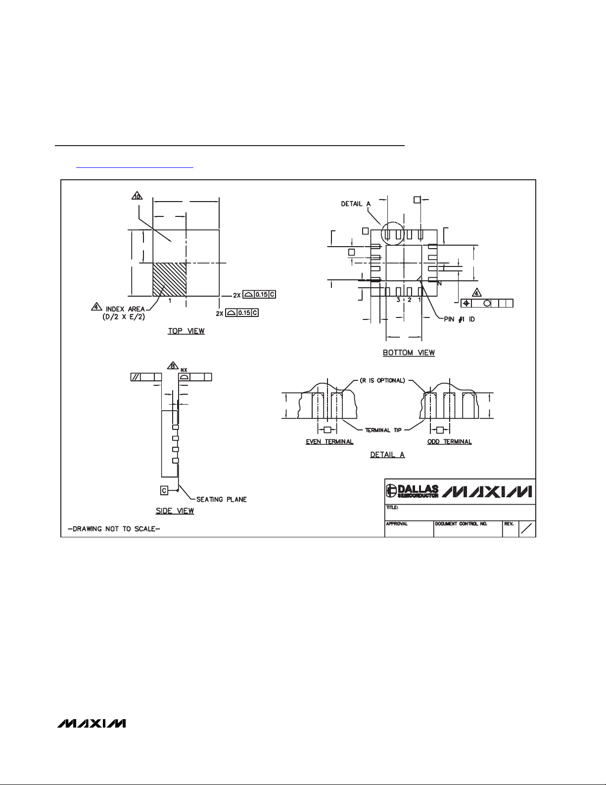
Package Information
(The package drawing(s) in this data sheet may not reflect the most current specifications. For the latest package outline information
go to www.maxim-ic.com/packages
.)
E/2
AAAA
L
(NE - 1) X e
E2/2
E2
D2/2
b
C
L
D2
0.10 M C A B
L
E
(ND - 1) X e
e
C
L
k
C
L
C
L
A
A2
A1
L
MARKING
D/2
D
0.10 C 0.08 C
12x16L QFN THIN.EPS
e
PACKAGE OUTLINE
8, 12, 16L THIN QFN, 3x3x0.8mm
e
21-0136
1
I
2
MAX3984
1Gbps to 10Gbps Preemphasis Driver with
Receive Equalizer
Maxim cannot assume responsibility for use of any circuitry other than circuitry entirely embodied in a Maxim product. No circuit patent licenses are
implied. Maxim reserves the right to change the circuitry and specifications without notice at any time.
18
____________________Maxim Integrated Products, 120 San Gabriel Drive, Sunnyvale, CA 94086 408-737-7600
© 2007 Maxim Integrated Products is a registered trademark of Maxim Integrated Products, Inc.
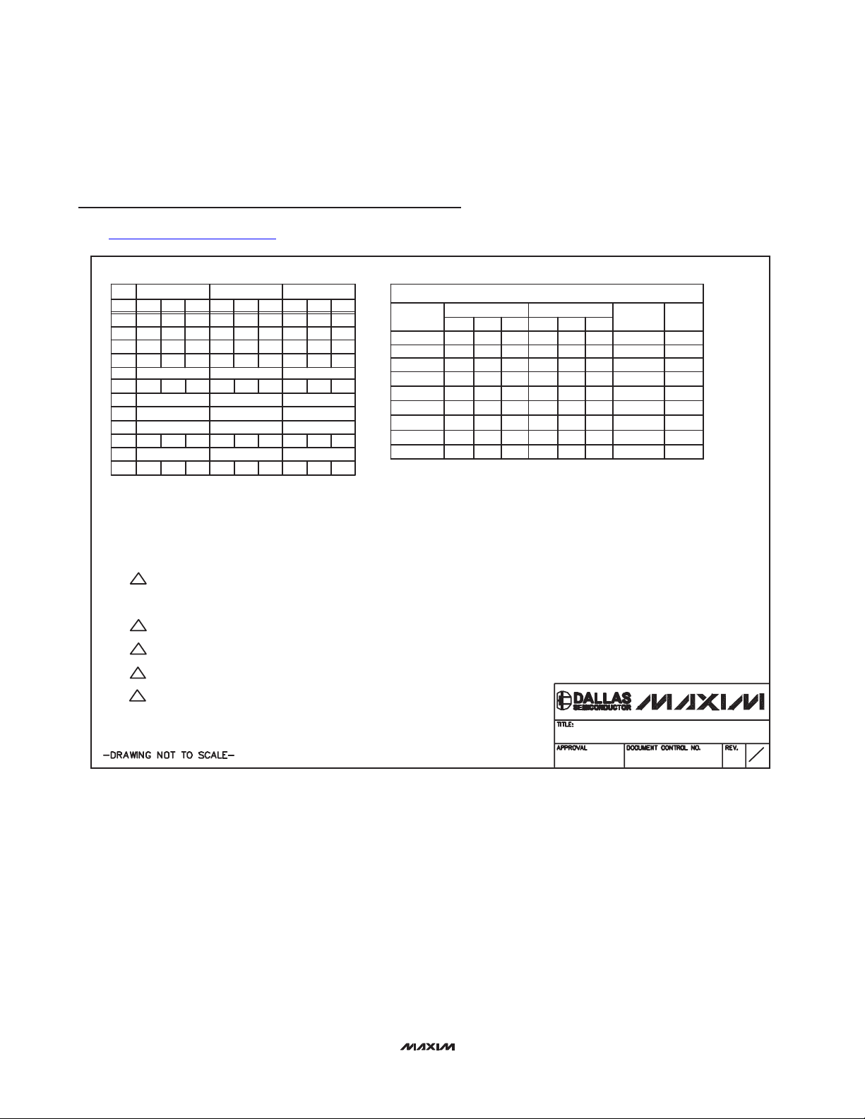
Package Information (continued)
(The package drawing(s) in this data sheet may not reflect the most current specifications. For the latest package outline information
go to www.maxim-ic.com/packages
.)
MIN.
0.70 0.75 0.80
A
b
0.25 0.30 0.35
2.90
D
2.90 3.00 3.10
E
e
0.35
L
ND
NE
0
A1
A2
k
0.25
8L 3x3
NOM. M
3.00 3.10
0.65 BSC.
0.55 0.75
8
2
2
0.02
0.20 REF
-
PKG
REF. MIN.
NOTES:
1. DIMENSIONING & TOLERANCING CONFORM TO ASME Y14.5M-1994.
2. ALL DIMENSIONS ARE IN MILLIMETERS. ANGLES ARE IN DEGREES.
3. N IS THE TOTAL NUMBER OF TERMINALS.
4. THE TERMINAL #1 IDENTIFIER AND TERMINAL NUMBERING CONVENTION SHALL CONFORM TO
JESD 95-1 SPP-012. DETAILS OF TERMINAL #1 IDENTIFIER ARE OPTIONAL, BUT MUST BE LOCATED
WITHIN THE ZONE INDICATED. THE TERMINAL #1 IDENTIFIER MAY BE EITHER A MOLD OR
MARKED FEATURE.
5. DIMENSION b APPLIES TO METALLIZED TERMINAL AND IS MEASURED BETWEEN 0.20 mm AND 0.25 mm
FROM TERMINAL TIP.
6. ND AND NE REFER TO THE NUMBER OF TERMINALS ON EACH D AND E SIDE RESPECTIVELY.
7. DEPOPULATION IS POSSIBLE IN A SYMMETRICAL FASHION.
8. COPLANARITY APPLIES TO THE EXPOSED HEAT SINK SLUG AS WELL AS THE TERMINALS.
9. DRAWING CONFORMS TO JEDEC MO220 REVISION C.
10. MARKING IS FOR PACKAGE ORIENTATION REFERENCE ONLY.
11. NUMBER OF LEADS SHOWN ARE FOR REFERENCE ONLY.
12. WARPAGE NOT TO EXCEED
0.05
AX.
12L 3x3
NOM. MAX. NOM.
0.70
0.20
2.90
2.90
0.50 BSC.
0.45
0
0.20 REF
-
0.25
0.75
0.25
3.00
3.00
0.55
0.02
12N
3
3
-
MIN. MAX.
0.80
0.30
2.90
3.10
3.10
0.65
0.30
0.05
-
0.25
0.10mm.
16L 3x3
0.70
0.20
2.90
0.50 BSC.
040.02
0.20 REF
0.75
0.25
3.00
3.00
0.40
EXPOSED PAD VARIATIONS
PKG.
0.80
0.30
3.10
3.10
0.50
16
4
0.05
-
-
CODES
TQ833-1 1.250.25 0.70 0.35 x 45° WEEC1.250.700.25
T1233-1
3
T1233-
T1233-4
T1633-2 0.95
T1633F-3
T1633FH-3 0.65 0.80 0.95
T1633-4 0.95
T1633-5 0.95
D2
MIN.
0.95
0.95
0.95
0.65
MAX.
NOM.
1.25
1.10
1.25
1.10
1.251.10
1.25
1.10
0.95
0.80
1.10 1.25 0.95 1.10
1.25
1.10
E2
NOM.
MIN.
0.95
0.95 1.10 0.35 x 45°1.25 WEED-1
0.95
0.65
0.65 0.80
MAX.
1.10
1.25
1.100.95
1.10
1.25
0.80
0.95
0.95
1.25
1.25
1.10
PACKAGE OUTLINE
8, 12, 16L THIN QFN, 3x3x0.8mm
ID
PIN
0.35 x 45°
0.35 x 45°
0.35 x 45°
0.225 x 45°
0.225 x 45°
0.35 x 45°
0.35 x 45°
JEDEC
WEED-1
WEED-11.25
WEED-2
WEED-2
WEED-2
WEED-2
WEED-20.95
21-0136
2
I
2
 Loading...