

Page 1
General Description
The MAX3980 quad equalizer provides compensation
for transmission medium losses for four “lanes” of digital NRZ data at a 3.125Gbps data rate in one package.
It is tailor-made for 10-Gigabit Ethernet (10GbE) backplane applications requiring attenuation of noise and jitter that occur in communicating from MAC to PMD or
from MAC to Switch. In support of the IEEE-802.3ae for
the XAUI interface, the MAX3980 adaptively allows
XAUI lanes to reach up to 40in (1.0m) on FR-4 board
material.
The equalizer has 100Ω differential CML data inputs
and outputs.
The MAX3980 is available in a 44-pin exposed-pad
QFN package. The MAX3980 consumes only 700mW at
+3.3V or 175mW per channel.
Applications
IEEE-802.3ae XAUI Interface (3.125Gbps)
InfiniBandSM(2.5Gbps)
Features
♦ Four Differential Digital Data “Lanes” at
3.125Gbps
♦ Spans 40in (1.0m) of FR-4 PC Board
♦ Receiver Equalization Reduces Intersymbol
Interference (ISI)
♦ Low-Power, 175mW per Channel
♦ Standby Mode—Power-Down State
♦ Single +3.3V Supply
♦ Signal Detect
MAX3980
3.125Gbps XAUI Quad Equalizer
________________________________________________________________
Maxim Integrated Products
1
Ordering Information
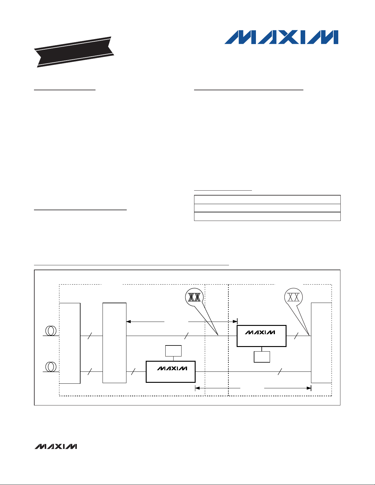
LINE CARD
PMD MAC
RxRxTx
Tx
RxRxTx
Tx
10GbE
4
4 4 4
4
4
4 x 3.125Gbps
4 x
3.125Gbps
SWITCH
Rx
Tx
≤ 40in (1.0m)
SWITCH CARD
MAX3980
OUT IN
+3.3V
SUPPLY
MAX3980
IN OUT
+3.3V
SUPPLY
PC BOARD
BACKPLANE
≤ 40in (1.0m)
Typical Application Circuit
19-2153; Rev 3; 12/08
For pricing, delivery, and ordering information, please contact Maxim Direct at 1-888-629-4642,
or visit Maxim’s website at www.maxim-ic.com.
Pin Configuration appears at end of data sheet.
EVALUATION KIT
AVAILABLE
+
Denotes a lead-free/RoHS-compliant package.
*
EP = Exposed pad.
InfiniBand is a trademark and service mark of the InfiniBand Trade Association.
PART TEMP RANGE PIN-PACKAGE
MAX3980UGH 0°C to +85°C 44 QFN-EP*
MAX3980UTH+ 0°C to +85°C 44 TQFN-EP*
Page 2
MAX3980
3.125Gbps XAUI Quad Equalizer
2 _______________________________________________________________________________________
ABSOLUTE MAXIMUM RATINGS
ELECTRICAL CHARACTERISTICS
(VCC= +3.0V to +3.6V, input data rate = 3.125Gbps, TA= 0°C to +85°C. Typical values are at VCC= +3.3V and TA= +25°C, unless
otherwise noted.)
Stresses beyond those listed under “Absolute Maximum Ratings” may cause permanent damage to the device. These are stress ratings only, and functional
operation of the device at these or any other conditions beyond those indicated in the operational sections of the specifications is not implied. Exposure to
absolute maximum rating conditions for extended periods may affect device reliability.
Supply Voltage, VCC..............................................-0.5V to +4.0V
Voltage at SDET, IN_±................................-0.5V to (V
CC
+ 0.5V)
Current Out of OUT_±.......................................-25mA to +25mA
Continuous Power Dissipation (T
A
= +85°C)
44-Pin QFN-EP (derate 26.3mW/°C above +85°C)...2105mW
Operating Ambient Temperature Range ................0°C to +85°C
Storage Temperature Range .............................-55°C to +150°C
Lead Temperature (soldering, 10s) .................................+300°C
Supply Power
Supply Noise Tolerance
Signal Detect Assert Input signal level to assert SDET (Note 1) 100 mVp-p
Signal Detect Deassert Input signal level to deassert SDET (Note 1) 30 mVp-p
Signal Detect Delay 10 μs
Latency From input to output 0.32 ns
CML RECEIVER INPUT
Input Voltage Swing
Return Loss 100MHz to 2.5GHz 12 dB
Input Resistance Differential 80 100 120 Ω
EQUALIZATION
Residual Jitter
Random Jitter (Note 2) 1.5 ps
CML TRANSMITTER OUTPUT (into 100Ω ±1Ω)
Output Voltage Swing Differential swing 550 850 mVp-p
Common-Mode Voltage VCC - 0.3 V
Transition Time tf, t
Differential Skew
Output Resistance Single ended 40 50 60 Ω
PARAMETER SYMBOL CONDITIONS MIN TYP MAX UNITS
EN = TTL low 0.25
EN = TTL high 0.7 0.9
10Hz < f < 100Hz 100
100Hz < f < 1MHz 40
1MHz < f < 2.5GHz 10
XAUI transmitter output measured
differentially at point A, Figure 1, using
K28.5 pattern
Total jitter (Note 2) 0.3
Deterministic jitter 0.2
20% to 80% (Note 3) 60 130 ps
r
Difference in 50% crossing between OUT_+
and OUT_-
200 800 mVp-p
12 ps
W
mVp-p
UIp-p
RMS
Page 3
MAX3980
3.125Gbps XAUI Quad Equalizer
_______________________________________________________________________________________ 3
ELECTRICAL CHARACTERISTICS (continued)
(VCC= +3.0V to +3.6V, input data rate = 3.125Gbps, TA= 0°C to +85°C. Typical values are at VCC= +3.3V and TA= +25°C, unless
otherwise noted.)
Note 1: K28.7 pattern is applied differentially at point A as shown in Figure 1.
Note 2: Total jitter does not include the signal source jitter. Total jitter (TJ) = [14.1 x RJ + DJ] where RJ is random RMS jitter and DJ
is maximum deterministic jitter. Signal source is a K28.5± pattern (00 1111 1010 11 0000 0101) for the deterministic jitter
test and K28.7 (0011111000) or equivalent for the random jitter test. Residual jitter is that which remains after equalizing
media-induced losses of the environment of Figure 1 or its equivalent. The deterministic jitter at point B must be from mediainduced loss and not from clock-source modulation. Jitter is measured at 0 at point C of Figure 1.
Note 3: Using K28.7 (0011111000) pattern.
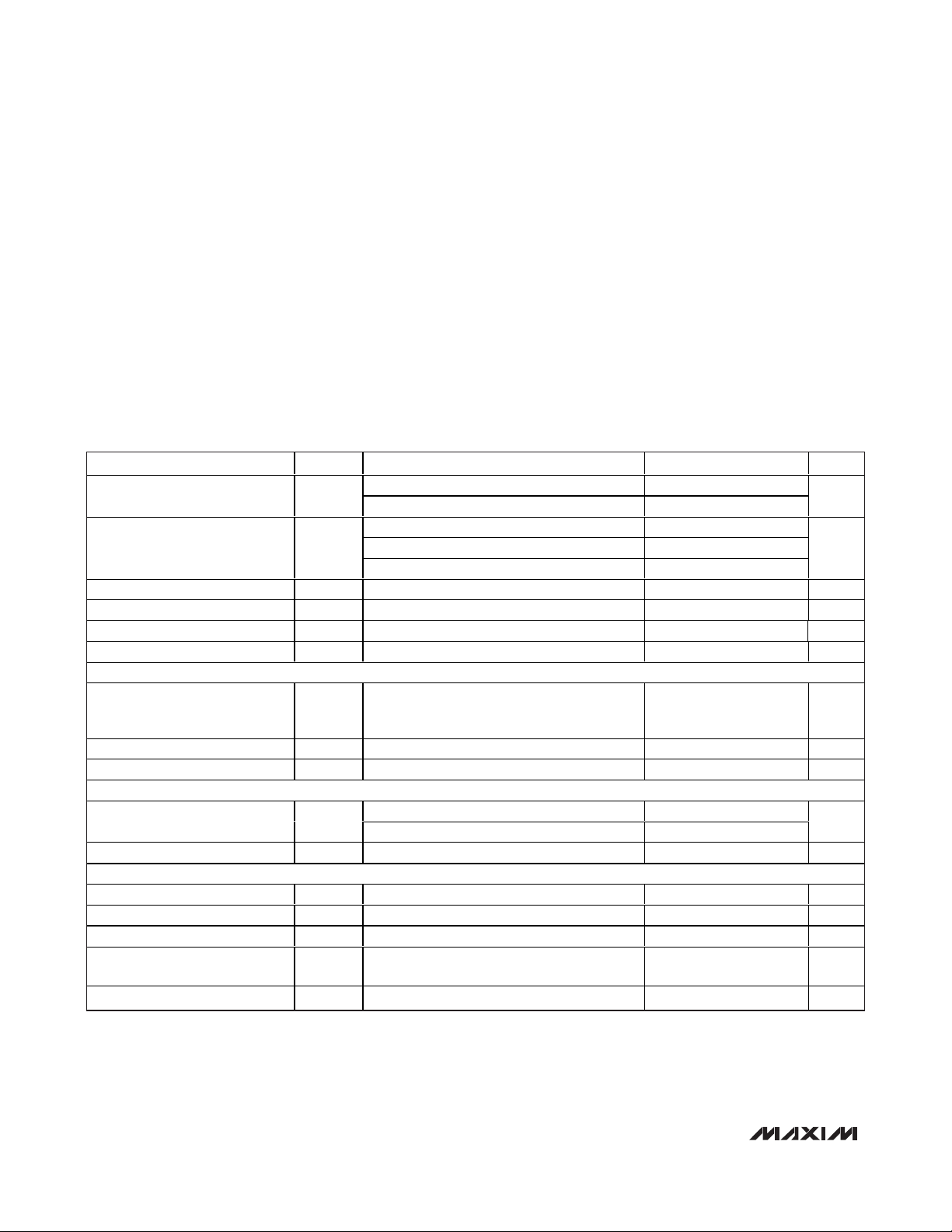
Figure 1. Test Conditions Referenced in the Electrical Characteristics Table
TTL CONTROL PINS
Input High Voltage 2.0 V
Input Low Voltage 0.8 V
Input High Current 250 μA
Input Low Current 500 μA
Output High Voltage Internal 10kΩ pullup 2.4 V
Output Low Voltage Internal 10kΩ pullup 0.4 V
PARAMETER SYMBOL CONDITIONS MIN TYP MAX UNITS
A
FR-4 STRIPLINE
SMA
CONNECTOR
B
≤ 40in (1m)
MAX3980
SMA
CONNECTOR
C
OUTIN
Page 4
MAX3980
3.125Gbps XAUI Quad Equalizer
4 _______________________________________________________________________________________
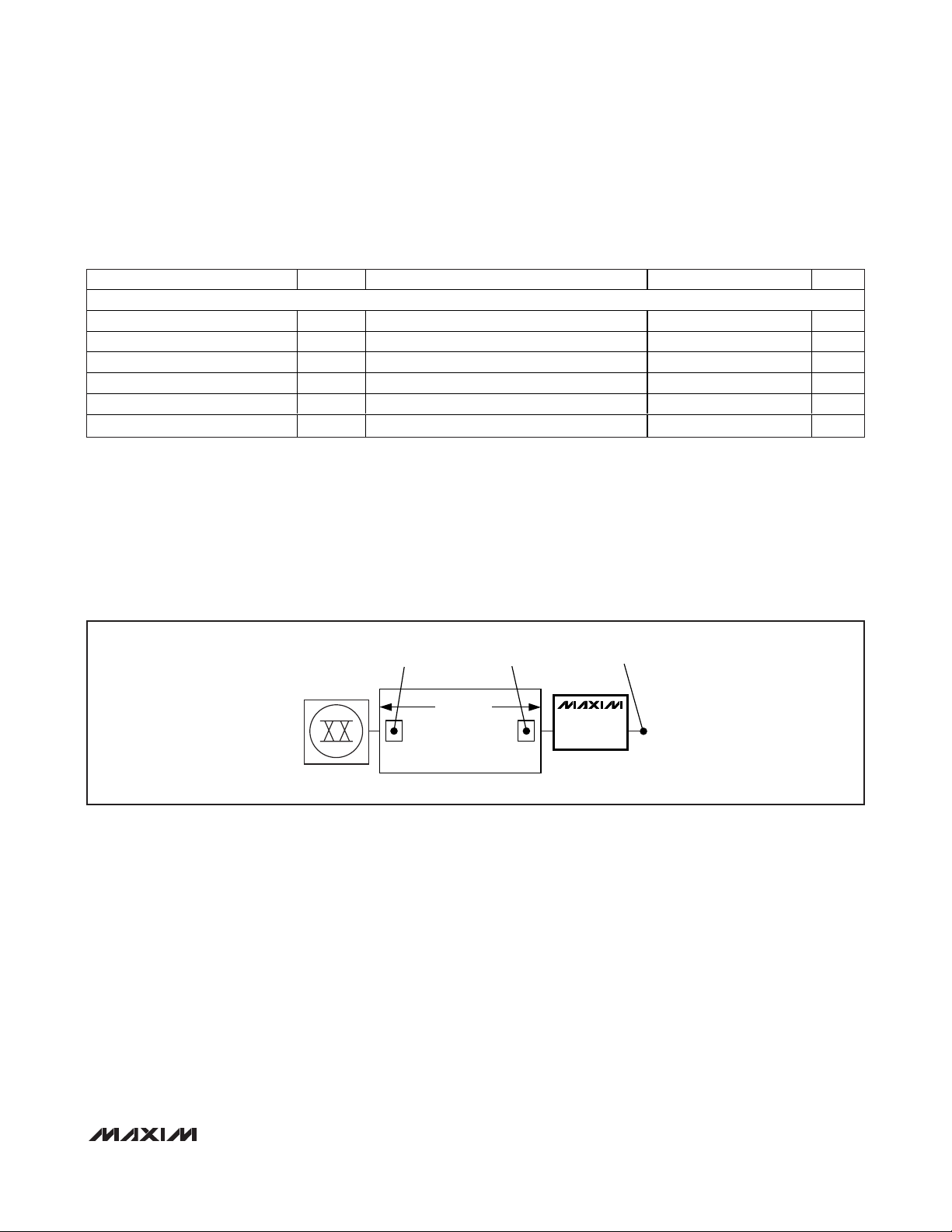
Typical Operating Characteristics
(VCC= +3.3V, 3.125Gbps, 500mVp-p board input with 27- 1 PRBS, TA= +25°C, unless otherwise noted.)
50mV/
div
50ps/div
EQUALIZER INPUT EYE DIAGRAM
BEFORE EQUALIZATION
(40in FR-4 6mil STRIPLINE)
MAX3980 toc01
100mV/
div
50ps/div
EQUALIZER OUTPUT EYE DIAGRAM
AFTER EQUALIZATION
(40in FR-4 6mil STRIPLINE)
MAX3980 toc02
100mV/
div
50ps/div
EQUALIZER OUTPUT EYE DIAGRAM
(20in BACKPLANE WITH TWO TERADYNE HSD
CONNECTORS AND 3in DAUGHTERBOARD)
MAX3980 toc03
-50
-30
-40
-10
-20
0
10
50
INPUT RETURN GAIN (S11, DIFFERENTIAL,
INPUT SIGNAL = -60dBm,
DEVICE POWERED OFF)
MAX3980 toc04
FREQUENCY (MHz)
GAIN (dB)
20501050 3050 4050 5050
0
35
30
25
20
15
10
5
40
EQUALIZER DETERMINISTIC JITTER
vs. LENGTH
(FR-4 6mil STRIPLINE, K28.5 PATTERN)
MAX3980 toc05
LENGTH (in)
JITTER (ps)
0203010
40
50
200
250
300
350
400
450
500
02010 30 40 50 60 70 80 90
EQUALIZER LATENCY
vs. TEMPERATURE
MAX3980 toc06
TEMPERATURE (°C)
DELAY (ps)
70
50
130
110
90
170
190
150
210
0304010 20 50 60 70 80
EQUALIZER OPERATING
CURRENT vs. TEMPERATURE
MAX3980 toc07
TEMPERATURE (°C)
CURRENT (mA)
NORMAL OPERATION
(EN = TTL HIGH)
STANDBY POWER
(EN = TTL LOW)
Page 5
MAX3980
3.125Gbps XAUI Quad Equalizer
_______________________________________________________________________________________ 5
Pin Description
PIN NAME FUNCTION
1, 5, 9, 13,
23, 27, 31,
35
2 IN1+ Positive Equalizer Input Channel 1, CML
3 IN1- Negative Equalizer Input Channel 1, CML
4, 8, 12, 16,
26, 30, 34,
38
6 IN2+ Positive Equalizer Input Channel 2, CML
7 IN2- Negative Equalizer Input Channel 2, CML
10 IN3+ Positive Equalizer Input Channel 3, CML
11 IN3- Negative Equalizer Input Channel 3, CML
14 IN4+ Positive Equalizer Input Channel 4, CML
15 IN4- Negative Equalizer Input Channel 4, CML
17–22, 39–42 N.C. No Connection. Leave unconnected.
24 OUT4- Negative Equaliz er Output Channel 4, CML
25 OUT4+ Positive Equali zer Output Channel 4, CML
28 OUT3- Negative Equaliz er Output Channel 3, CML
29 OUT3+ Positive Equali zer Output Channel 3, CML
32 OUT2- Negative Equaliz er Output Channel 2, CML
33 OUT2+ Positive Equali zer Output Channel 2, CML
36 OUT1- Negative Equaliz er Output Channel 1, CML
37 OUT1+ Positive Equali zer Output Channel 1, CML
43 EN
44 SDET Signal Detect Output for Channel 1. Produces a TTL high output when a signal is detected.
— EP
V
CC
GND Suppl y Ground
+3.3V Supply Voltage
Enable Equalizer Input. A TTL high se lects normal operation. A TTL low selects low-power
standby mode.
Exposed Pad. The exposed pad must be soldered to the circuit board ground plane for proper
thermal and electrical performance.
Page 6
MAX3980
Detailed Description
Receiver and Transmitter
The receiver accepts four lanes of 3.125Gbps currentmode logic (CML) digital data signals. The adaptive
equalizer compensates each received signal for dielectric and skin losses. The limiting amp shapes the output
of the equalizer. The regenerated XAUI lanes are transmitted as CML signals. The source impedance and termination impedances are 100Ω differential.
General Theory of Operation
Internally, the MAX3980 comprises signal-detect circuitry, four matched equalizers, and one equalizercontrol loop. The four equalizers are made up of a master equalizer and three slave equalizers. The adaptive
control is generated from only channel 1. It is assumed
that all channels have the same characterization in frequency content, coding, and transmission length.
The master equalizer consists of the following functions:
signal detect, adaptive equalizer, equalizer control, and
limiting and output drivers. The signal detect indicates
input signal power. When the input signal level is sufficiently high, the SDET output is asserted. This does not
directly control the operation of the part.
The equalizer core reduces intersymbol interference
(ISI), compensating for frequency-dependent, mediainduced loss. The equalization control detects the
spectral contents of the input signal and provides a
control voltage to the equalizer core, adapting it to different media. The equalizer operation is optimized for
short-run DC-balanced transmission codes such as
8b/10b codes.
CML Input and Output Buffers
The input and output buffers are implemented using
CML. Equivalent circuits are shown in Figures 2 and 3.
For details on interfacing with CML, see Maxim application note HFAN-1.0,
Interfacing Between CML, PECL,
and LVDS
. The common-mode voltage of the input and
output is above 2.5V. AC-coupling capacitors are
required when interfacing this part. Values of 0.10µF or
greater are recommended.
Media Equalization
Equalization at the input port compensates for the highfrequency loss encountered with up to 40in (1.0m) of
FR-4 transmission lines. This part is optimized for 40in
and 3.125Gbps; however, the part reduces ISI for signals spanning longer distances and functions for data
rates from 2Gbps to 4Gbps, provided that short-length
balanced codes, such as 8b/10b, are used.
Applications Information
Standby Mode
The power-saver standby state allows reduced-power
operation. The TTL input, EN, must be set to TTL high
for normal operation. A TTL low at EN forces the equalizer into the standby state. The signal EN does not
affect the operation of the signal detect (SDET) function. For constant operation, connect the EN signal
directly to VCC.
3.125Gbps XAUI Quad Equalizer
6 _______________________________________________________________________________________
Functional Diagram
IP1, IN1 ONLY
IN1+
2
3
IN1-
4
2
3
4
EN
2
3
4
SDET FUNCTION IS
INDEPENDENT OF EN
EQUALIZER
POWER
MANAGEMENT
SIGNAL
DETECT
2
TTL
LIMITING
AMP
3
4
MAX3980
2
3
4
CML
2
3
4
SDET
OUT1+
OUT1-
2
3
4
2
3
4
Page 7
Signal Detect with Standby Mode
Signal activity is detected on channel 1 only. When the
peak-to-peak differential voltage at IN1± is less than
30mVp-p, the TTL output SDET goes low. When the
peak-to-peak differential voltage becomes greater than
100mVp-p, SDET is asserted high. SDET can be used
to automatically force the equalizer into standby mode
by connecting SDET directly to the EN input. When not
used, SDET should not be connected.
The signal-detect function continues to operate while
the part is in standby mode. While connected to the EN
pin, the signal detect can “wake up” the part and
resume normal operation.
Layout Considerations
Circuit-board layout and design can significantly affect
the MAX3980 performance. Use good high-frequency
design techniques, including minimizing ground inductances and vias and using controlled-impedance transmission lines for the high-frequency data signals.
Signals should be routed differentially to reduce EMI
susceptibility and crosstalk. Power-supply decoupling
capacitors should be placed as close as possible to
the V
CC
pins.
MAX3980
3.125Gbps XAUI Quad Equalizer
_______________________________________________________________________________________ 7
Figure 2. CML Input Buffer
Figure 3. CML Output Buffer
V
CC
1.2kΩ
50Ω50Ω
IN+
IN-
200μA
ESD
STRUCTURES
V
CC
50Ω50Ω
OUT+
OUT-
Q1 Q2
DATA
ESD
STRUCTURES
Page 8

MAX3980
3.125Gbps XAUI Quad Equalizer
8 _______________________________________________________________________________________
Pin Configuration Package Information
For the latest package outline information and land patterns, go
to www.maxim-ic.com/packages
.
PACKAGE TYPE PACKAGE CODE DOCUMENT NO.
44 QFN G4477-1
21-0092
44 TQFN T4477-3
21-0144
TOP VIEW
EN
N.C.
N.C.
N.C.
N.C.
MAX3980
N.C.
GND
GND
N.C.
SDET
4443424140393837363534
1
V
CC
2
IN1+
IN1-
GND
V
IN2+
IN2-
GND
V
IN3+
IN3-
3
4
5
CC
6
7
8
9
CC
10
*EP
11
1213141516171819202122
GND
CC
V
IN4-
IN4+
QFN-EP/TQFN-EP
*NOTE: THE EXPOSED PAD MUST BE SOLDERED TO SUPPLY GROUND.
OUT1+
N.C.
OUT1-
N.C.
CC
V
N.C.
GND
N.C.
33
OUT2+
32
OUT2-
31
V
CC
30
GND
OUT3+
29
OUT3-
28
V
27
CC
GND
26
OUT4+
25
OUT4-
24
V
23
CC
Page 9
MAX3980
3.125Gbps XAUI Quad Equalizer
Maxim cannot assume responsibility for use of any circuitry other than circuitry entirely embodied in a Maxim product. No circuit patent licenses are
implied. Maxim reserves the right to change the circuitry and specifications without notice at any time.
Maxim Integrated Products, 120 San Gabriel Drive, Sunnyvale, CA 94086 408-737-7600 _____________________
9
© 2008 Maxim Integrated Products is a registered trademark of Maxim Integrated Products, Inc.
Revision History
REVISION
NUMBER
0 9/01 Initial release. —
1 5/03
2 1/05
3 12/08
REVISION
DATE
DESCRIPTION
Added the package code to the Ordering Information table. 1
Updated the 21-0092 package drawing in the Package Information section. 8, 9
Added the TQFN package to the Ordering Information table. 1
Added the 21-0144 package drawing to the Pac kage Information section. 10
Changed the Absolute Maximum Ratings of SDET, IN_± from +5.0V to (V
0.5V) to –5.0V to (V
to 0.5V).
CC
CC
to
PAGES
CHANGED
2
 Loading...