

Page 1
19-5144; Rev 0; 2/10
可提供评估板
1.0625Gbps至11.3Gbps、
MAX3945
电,优化用于光纤通道以及以太网发送系统,数据速率高
达
11.3Gbps
号进行限幅,产生
和输出
双通 道限幅放 大器带有可编程滤波器,能够针对不同数据
速率下的敏感度进行优化,抑制光学系统可能产生的驰豫
振荡。
个可编程时间屏蔽的
线数字接口减少了引脚数,无需外部器件即可实现
3
限、
接收
多速率、低功耗 限幅放 大器采用
。高灵敏度限幅放大器对互阻放大器产生的信
电平差分输出信号。所有差分输入
CML
都优化于
(I/O)
MAX3945
极性、
LOS
极性、Rx输入滤波器以及Rx去加重的控制。
(Rx)
集成了两路信号丢失
LOS
背向端接
50
Ω
输出。
LOS
模式、
传输线。
PCB
(LOS)
输出电平、输入失调修正、
CML
+3.3V
检测电路和一
MAX3945采用3mmx3mm、16引脚TQFN
1x/2x/4x/8xSFF/SFP/SFP+MSA
10GBASE-SR/LRSFP+
光收发器
光纤通道光收发器
电源供
MAX3945
LOS
封装。
概述
门
应用
10GPONONU
PART TEMP RANGE PIN-PACKAGE
MAX3945ETE+
表示无铅
+
*
EP=
典型应用电路在数据资料的最后给出。
(Pb)/符合RoHS
裸焊盘。
-40NC to +85NC
标准的封装。
定购信息
16 TQFN-EP*
SFP+
双通道限幅放大器
S
130mW
S
单模块设计兼容于
LR
S
采用10.32Gbps ROSA,在1.25Gbps
度为
S
RATE_SEL = 0
3GHz
S
支持SFF-8431 SFP+ MSA和SFF-8472
S
3.3V
130mW
S
3.3V
154mW
S
11.3Gbps
S
RATE_SEL = 1、11.3Gbps
S
RATE_SEL = 1、8.5Gbps
S
RATE_SEL = 0、BW1 = 1、BW0 = 1、4.25Gbps
下具有
S
RATE_SEL = 0、BW1 = 0、BW0 = 0、1.25Gbps
下具有
S
RATE_SEL = 1
S
RATE_SEL = 0
S
CML
S
可编程
S
CML
S
LOS
S
LOS
S
可调节
S
可选择基于Rx输入的
S
3
功耗支持低于1W的
1000BASE-SX/LX和10GBASE-SR/
标准
-25.3dBm
时,可选择
输入滤波器
供电并提供基于
供电并提供基于Rx输入的
5ps
9.0ps
输出具有电平调节和禁止模式
CML
输出极性选择
极性选择
输出带有可编程屏蔽时间
LOS触发/
速率下具有
DJ
P-P
DJ
P-P
时,具有
时,具有
输出去加重
清除电平
RSSI
4mV
LOS
线数字接口与
Maxim SFP+
模块设计
SFP+
下光信号检测灵敏
1GHz/2.1GHz/2.5GHz/
数字诊断
监测的
输入灵敏度
P-P
速率下具有
速率下具有
26ps
52ps
功能时,总功耗为
LOS
功能时,总功耗为
LOS
4ps
P-P
4ps
P-P
上升和下降时间
上升和下降时间
或基于
系列产品兼容
RSSI
监测的
DJ
DJ
LOS
特性
速率
速率
MAX3945
_______________________________________________________________ Maxim Integrated Products 1
本文是英文数据资料的译文,文中可能存在翻译上的不准确或错误。如需进一步确认,请在您的设计中参考英文资料。
有关价格、供货及订购信息,请联络
或访问
Maxim
的中文网站:
china.maxim-ic.com
Maxim
亚洲销售中心:
。
10800 852 1249 (
北中国区),
10800 152 1249 (
南中国区),
Page 2
1.0625Gbps至11.3Gbps、
SFP+
双通道限幅放大器
ABSOLUTE MAXIMUM RATINGS
VCC ....................................................................... -0.3V to +4.0V
Voltage Range at SDA, SCL, CSEL,
LOS, CAZ, RPMIN ................................. -0.3V to (V
Voltage Range at ROUT+, ROUT- ........(V
Voltage Range at RIN+, RIN- ........ (V
Current Range Into LOS ...................................... -1mA to +5mA
Current Range Into SDA ..................................... -1mA to +1mA
MAX3945
Stresses beyond those listed under “Absolute Maximum Ratings” may cause permanent damage to the device. These are stress ratings only, and functional
operation of the device at these or any other conditions beyond those indicated in the operational sections of the specifications is not implied. Exposure to absolute
maximum rating conditions for extended periods may affect device reliability.
- 2V) to (VCC + 0.3V)
CC
- 1.7V) to (VCC + 0.3V)
CC
+ 0.3V)
CC
Current Out of ROUT+, ROUT- ..........................................40mA
Continuous Power Dissipation (T
16-Pin TQFN (derate 14.7mW/NC above +70NC) ......... 1.176W
Operating Junction Temperature Range ......... -55NC to +150NC
Storage Temperature Range ............................ -65NC to +160NC
Lead Temperature (soldering, 10s) ................................+300NC
Soldering Temperature (reflow) ......................................+260NC
= +70NC)
A
ELECTRICAL CHARACTERISTICS
(VCC = 2.85V to 3.63V, CML receiver output is AC-coupled to differential 100I load, C
are set to default values, unless otherwise noted. Typical values are at V
PARAMETER SYMBOL CONDITIONS MIN TYP MAX UNITS
POWER SUPPLY
Includes the CML output current,
V
DIFF_ROUT
Power-Supply Current I
Power-Supply Voltage V
Power-Supply Noise
GENERAL
Input Data Rate 1.06 10.32 11.3 Gbps
Input/Output SNR 14.1
BER 10E-12
POWER-ON RESET (POR)
POR Deassert Threshold 2.55 2.75 V
POR Assert Threshold 2.3 2.45 V
INPUT SPECIFICATIONS
Differential Input Resistance
RIN+/RIN-
Input Sensitivity
(Note 1)
Input Overload V
Input Return Loss
RPMIN Input-Current High I
CC
CC
R
IN_DIFF
V
INMIN
INMAX
SDD11
SCC11
IH
LOS1_EN = 1, LOS2_EN = 0
Includes the CML output current,
V
DIFF_ROUT
LOS1_EN = 0, LOS2_EN = 1
f < 10MHz 100
10MHz < f < 20MHz 10
RATE_SEL = 1, input transition time 25ps,
10.32Gbps, PRBS23-1 pattern
RATE_SEL = 0, input transition time 260ps,
1.25Gbps, K28.5 pattern
DUT is powered on, f P 5GHz
DUT is powered on, f P 16GHz
DUT is powered on, 1GHz < f P 5GHz
DUT is powered on, 1GHz < f P 16GHz
LOS1_EN = 0 and LOS2_EN = 1,
V
RPMIN
= 400mV
= 400mV
= 2V
= 3.3V, TA = +25NC, unless otherwise noted.)
CC
, RXDE_EN = 0,
P-P
, RXDE_EN = 0,
P-P
= 0.1FF, TA = -40NC to +85NC. Registers
CAZ
46.6 62
39.4 52.5
2.85 3.63 V
75 100 125
4 8
1 2
1.2 V
10
7
13
5
50 nA
mV
mV
mA
P-P
I
P-P
P-P
dB
dB
2 ______________________________________________________________________________________
Page 3
1.0625Gbps至11.3Gbps、
SFP+
双通道限幅放大器
ELECTRICAL CHARACTERISTICS (continued)
(VCC = 2.85V to 3.63V, CML receiver output is AC-coupled to differential 100I load, C
are set to default values, unless otherwise noted. Typical values are at V
PARAMETER SYMBOL CONDITIONS MIN TYP MAX UNITS
External RPMIN Filter Capacitor 100 pF
OUTPUT SPECIFICATIONS
Differential Output Resistance
ROUT+/ROUT-
Output Return Loss
Differential Output-Voltage High
Differential Output-Voltage
Medium
SET_CML DAC Range 60 255 Decimal
Differential Output Signal When
Squelched (Note 1)
Data Output Transition Time
(20% to 80%) (Note 1)
TRANSFER CHARACTERISTICS
Deterministic Jitter
(Notes 1, 2)
R
OUTDIFF
SDD22
SCC22
t
R/tF
DJ
DUT is powered on, f P 5GHz
DUT is powered on, f P 16GHz
DUT is powered on, 1GHz < f P 5GHz
DUT is powered on, 1GHz < f P 16GHz
5mV
P VIN P 1200mV
P-P
SET_CML[7:0] = 169d (decimal)
10mV
SET_CML[7:0] = 181d
10mV
RATE_SEL = 1, SET_CML[7:0] = 91d
Outputs AC-coupled, SET_CML[7:0] =
181d, at 8.5Gbps, SQ_EN = 1
60mV
RATE_SEL = 1, V
RXDE_EN = 0, input transition time 25ps,
pattern 11110000
10mV
RATE_SEL = 0, V
input transition time 260ps, pattern 11110000
10mV
RATE_SEL = 1, V
RXDE_EN = 0, input transition time 28ps
60mV
RATE_SEL = 1, V
RXDE_EN = 0, input transition time 28ps
60mV
RATE_SEL = 1, V
RXDE_EN = 0, input transition time 28ps
10mV
RATE_SEL = 0, BW1 = 0, BW0 = 0,
V
time 260ps
10mV
RATE_SEL = 0, BW1 = 1, BW0 = 1,
V
time 28ps
P VIN P 1200mV, RATE_SEL = 1,
P-P
P VIN P 1200mV
P-P
P VIN P 400mV
P-P
DIFF_ROUT
P VIN P 1200mV
P-P
DIFF_ROUT
P VIN P 1200mV
P-P
DIFF_ROUT
P VIN P 400mV
P-P
DIFF_ROUT
P VIN P 400mV
P-P
DIFF_ROUT
P VIN P 1200mV
P-P
DIFF_ROUT
DIFF_ROUT
= 800mV
P VIN P 1200mV
P-P
= 800mV
= 3.3V, TA = +25NC, unless otherwise noted.)
CC
, RATE_SEL = 0,
P-P
P-P,
at 10.32Gbps,
P-P
= 400mV
at 1.25Gbps,
P-P
= 800mV
at 8.5Gbps,
P-P
= 400mV
at 10.32Gbps,
P-P
= 400mV
at 11.3Gbps,
P-P
= 400mV
at 1.25Gbps,
P-P
, input transition
P-P
at 4.25Gbps,
P-P
, input transition
P-P
= 0.1FF, TA = -40NC to +85NC. Registers
CAZ
75 100 125
13
7
10
6
595 800 1005
595 800 1005
300 400 515 mV
6 15 mV
,
P-P
P-P
P-P
P-P
P-P
,
,
,
,
26 35
52 90
4 8
4 9
4 9
9 30
5 10
mV
ps
I
dB
P-P
P-P
P-P
ps
P-P
MAX3945
_______________________________________________________________________________________ 3
Page 4
1.0625Gbps至11.3Gbps、
SFP+
双通道限幅放大器
ELECTRICAL CHARACTERISTICS (continued)
(VCC = 2.85V to 3.63V, CML receiver output is AC-coupled to differential 100I load, C
are set to default values, unless otherwise noted. Typical values are at V
PARAMETER SYMBOL CONDITIONS MIN TYP MAX UNITS
Input = 60mV
Random Jitter
(Note 1)
MAX3945
Low-Frequency Cutoff
(Simulated Value)
Small-Signal Bandwidth
(Simulated Value)
Rx INPUT-BASED LOS SPECIFICATIONS (LOS1_EN = 1 and LOS2_EN = 0) (Note 1)
LOS Assert Sensitivity Range (Note 3) 14 77 mV
SET_LOS DAC Range 7 63 Decimal
LOS Hysteresis 10log(V
LOS Assert/Deassert Time (Note 4) 2.3 20 80
Low Assert Level
Low Deassert Level 14 18 22
Medium Assert Level
Medium Deassert Level 65 82 95
High Assert Level
High Deassert Level 127 158 182
LOS Output Masking Time
Range
LOS Output Masking DAC
Resolution
RSSI MONITOR-BASED LOS SPECIFICATIONS (LOS1_EN = 0 and LOS2_EN = 1) (Note 1)
LOS Assert Sensitivity Range (Note 5) 8.3 90 mV
SET_LOS DAC Range 4 63 Decimal
LOS Hysteresis 10log(V
LOS Assert/Deassert Time (Note 4) 2.3 20 80
Low Assert Level
Low Deassert Level 9.0 10.8 12.7
Medium Assert Level
Medium Deassert Level 77 85 92
High Assert Level
High Deassert Level 153 167 180
LOS Output Masking Time
Range
LOS Output Masking DAC
Resolution
RJ
f
3dB
RATE_SEL = 1, RXDE_EN = 0, input transi-
tion time 28ps, pattern 11110000,
V
DIFF_ROUT
RATE_SEL = 0, C
RATE_SEL = 1, C
RATE_SEL = 0, BW1 = 0, BW0 = 0 1.0
RATE_SEL = 0, BW1 = 0, BW0 = 1 2.1
RATE_SEL = 0, BW1 = 1, BW0 = 0 2.5
RATE_SEL = 0, BW1 = 1, BW0 = 1 3.0
RATE_SEL = 1 9
DEASSERT/VASSERT
SET_LOS[5:0] = 7d (Note 3)
SET_LOS[5:0] = 32d (Note 3)
SET_LOS[5:0] = 63d (Note 3)
SET_LOSTIMER[6:0] = 0d for minimum and
SET_LOSTIMER[6:0] = 127d for maximum
SET_LOSTIMER[6:0] = 1d to 127d 23 35 50
DEASSERT/VASSERT
SET_LOS[5:0] = 4d (Note 5)
SET_LOS[5:0] = 32d (Note 5)
SET_LOS[5:0] = 63d (Note 5)
SET_LOSTIMER[6:0] = 0d for minimum and
SET_LOSTIMER[6:0] = 127d for maximum
SET_LOSTIMER[6:0] = 1d to 127d 23 35 50
at 10.32Gbps,
P-P
= 800mV
CAZ
CAZ
= 3.3V, TA = +25NC, unless otherwise noted.)
CC
P-P
= 0.1FF
= 0.1FF
) 1.25 2.1 dB
) 1.25 2.1 dB
= 0.1FF, TA = -40NC to +85NC. Registers
CAZ
0.28 0.51 ps
2
0.7
8 11 14
39 49 58
77 96 112
0 2920
5.1 6.7 8.3
45 50 55
90 98 106
0 2920
kHz
GHz
mV
mV
mV
RMS
P-P
Fs
P-P
P-P
P-P
Fs
Fs
Fs
mV
mV
mV
Fs
Fs
4 ______________________________________________________________________________________
Page 5

1.0625Gbps至11.3Gbps、
SFP+
ELECTRICAL CHARACTERISTICS (continued)
(VCC = 2.85V to 3.63V, CML receiver output is AC-coupled to differential 100I load, C
are set to default values, unless otherwise noted. Typical values are at V
PARAMETER SYMBOL CONDITIONS MIN TYP MAX UNITS
OUTPUT LEVEL VOLTAGE DAC (SET_CML)
100I differential resistive load,
RXDE_EN = 0
Full-Scale Voltage V
Resolution
Integral Nonlinearity INL SET_CML[7:0] > 60d
LOS THRESHOLD VOLTAGE DAC (SET_LOS)
Full-Scale Voltage V
Resolution
Integral Nonlinearity INL SET_LOS[5:0] > 3d
CONTROL I/O SPECIFICATIONS
LOS Output High Voltage V
LOS Output Low Voltage V
3-WIRE DIGITAL I/O SPECIFICATIONS (SDA, CSEL, SCL)
Input High Voltage V
Input Low Voltage V
Input Hysteresis V
Input Leakage Current I
Output High Voltage V
Output Low Voltage V
3-WIRE DIGITAL INTERFACE TIMING CHARACTERISTICS (see Figure 5)
SCL Clock Frequency f
SCL Pulse-Width High t
SCL Pulse-Width Low t
SDA Setup Time t
SDA Hold Time t
SCL Rise to SDA Propagation
Time
CSEL Pulse-Width Low t
FS
FS
OH
OL
IH
IL
HYST
IL,IH
OH
OL
SCL
CH
CL
DS
DH
t
D
CSW
100I differential resistive load,
RATE_SEL = 1, RXDE_EN = 1, RXDE1 = 1,
RXDE0 = 1 (maximum deemphasis)
100I differential resistive load,
RXDE_EN = 0
100I differential resistive load,
RATE_SEL = 1, RXDE_EN = 1, RXDE1 = 1,
RXDE0 = 1 (maximum deemphasis)
LOS1_EN = 1, LOS2_EN = 0 96 mV
LOS1_EN = 0, LOS2_EN = 1 98 mV
LOS1_EN = 1, LOS2_EN = 0 1.52 mV
LOS1_EN = 0, LOS2_EN = 1 1.56 mV
R
= 4.7kI to 10kI to V
LOS
R
= 4.7kI to 10kI to V
LOS
VIN = 0V or VCC, internal pullup or
pulldown (75kI typ)
External pullup of 4.7kI to V
External pullup of 4.7kI to V
= 3.3V, TA = +25NC, unless otherwise noted.)
CC
CC
CC
CC
CC
双通道限幅放大器
= 0.1FF, TA = -40NC to +85NC. Registers
CAZ
1192
828
4.5
3.3
Q0.9
Q0.7
VCC -
0.5
0 0.4 V
2.0 V
0.082 V
VCC -
0.5
0 0.4 V
0 400 1000 kHz
500 ns
500 ns
100 ns
100 ns
500 ns
V
CC
CC
0.8 V
85
V
CC
5 ns
mV
mV
LSB
LSB
MAX3945
P-P
P-P
P-P
P-P
V
V
FA
V
_______________________________________________________________________________________ 5
Page 6
1.0625Gbps至11.3Gbps、
SFP+
双通道限幅放大器
ELECTRICAL CHARACTERISTICS (continued)
(VCC = 2.85V to 3.63V, CML receiver output is AC-coupled to differential 100I load, C
are set to default values, unless otherwise noted. Typical values are at V
PARAMETER SYMBOL CONDITIONS MIN TYP MAX UNITS
CSEL Leading Time Before the
First SCL Edge
MAX3945
CSEL Trailing Time After the Last
SCL Edge
SDA, SCL External Load C
Note 1: Guaranteed by design and characterization, T
Note 2: Deterministic jitter is measured with a repeating K28.5 pattern [00111110101100000101] for 1.25Gbps to 8.5Gbps data.
At 10.32Gbps and 11.3Gbps, a repeating K28.5 plus 59 0s and K28.5 plus 59 1s pattern is used. Deterministic jitter is
defined as the arithmetic sum of pulse-width distortion (PWD) and pattern-dependent jitter (PDJ).
Note 3: LOS1_EN = 1, data rates of 1.25Gbps to 8.5Gbps with K28.5 pattern, and 6.4GHz input filter. For data rates of 10.32Gbps
to 11.3Gbps, the input filter is 12.5GHz and the pattern is PRBS23-1.
Note 4: Measurement includes an input AC-coupling capacitor of 100nF and C
is switched between two amplitudes: Signal_ON and Signal_OFF.
1) Receiver operates at sensitivity level plus 1dB power penalty
a) Signal_OFF = 0
Signal_ON = (+8dB) + 10log(min_assert_level)
b) Signal_ON = (+1dB) + 10log(max_deassert_level)
Signal_OFF = 0
2) Receiver operates at overload
Signal_OFF = 0
Signal_ON = 1.2V
max_deassert_level and min_assert_level are measured for one SET_LOS setting
Note 5: LOS1_EN = 0, LOS2_EN = 1, DC voltage applied to the RPMIN input.
P-P
t
L
t
T
Total bus capacitance on one line with
B
4.7kI to V
CC
= -40NC to +95NC.
A
= 3.3V, TA = +25NC, unless otherwise noted.)
CC
CAZ
= 0.1FF, TA = -40NC to +85NC. Registers
CAZ
500 ns
500 ns
20 pF
of 100nF. The signal at the RIN or RPMIN input
6 ______________________________________________________________________________________
Page 7
1.0625Gbps至11.3Gbps、
MAX3945 toc04
-21
SFP+
双通道限幅放大器
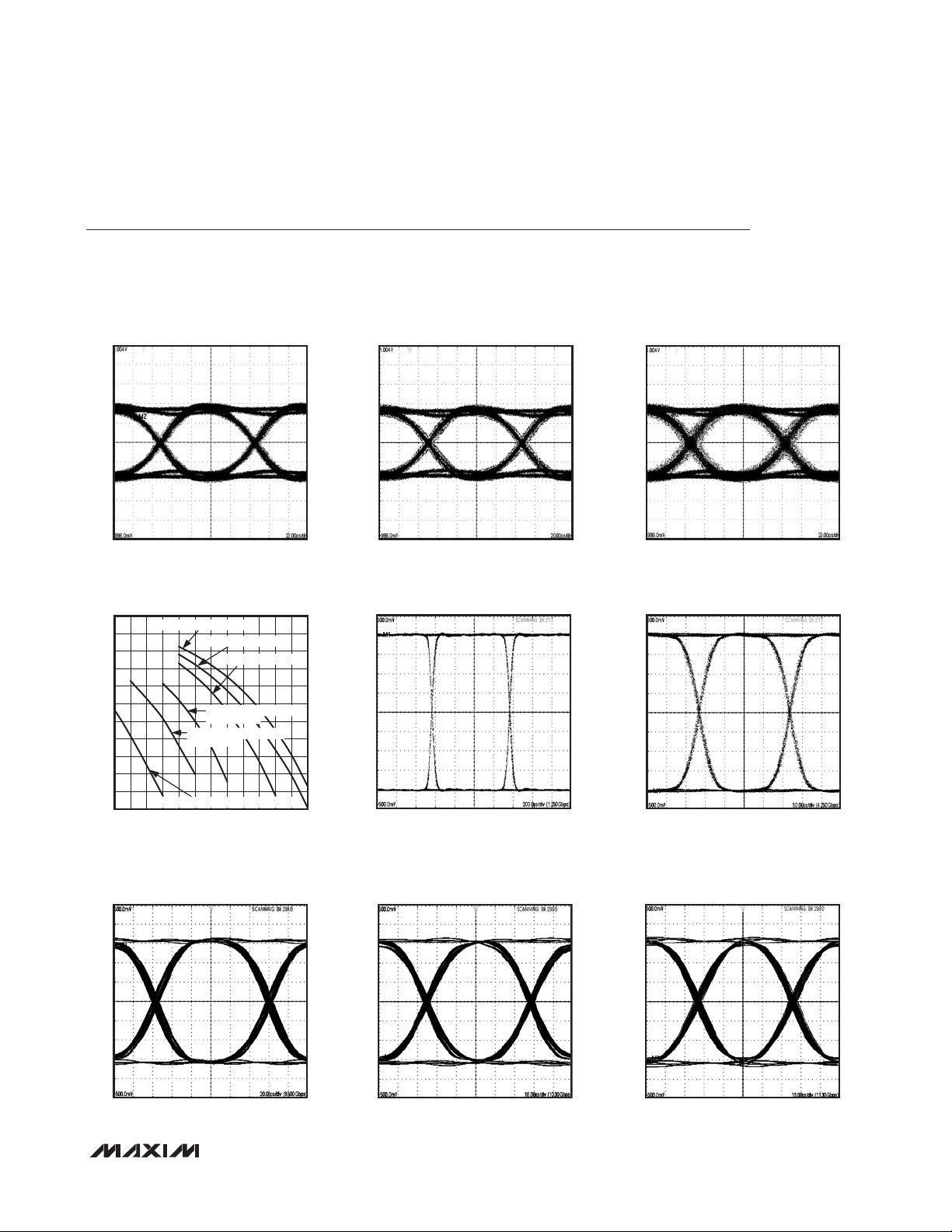
典型工作特性
(VCC = 3.3V, TA = +25NC, unless otherwise noted. Registers are set to default values, unless otherwise noted, and the 3-wire interface
is static during measurements.)
RECEIVE OUTPUT FROM OPTICAL SYSTEM,
10.32Gbps, OPTICAL INPUT -10dBm,
RXDE1 = 1, RXDE0 = 0
MAX3945 toc01
OPTICAL BER CURVES (NEC NR3312)
1.00E-01
1.00E-02
1.00E-03
1.00E-04
1.00E-05
1.00E-06
BER
1.00E-07
1.00E-08
1.00E-09
1.00E-10
1.00E-11
1.00E-12
-27
10.3Gbps, PRBS31, RATE_SEL = 1
8.5Gbps, PRBS9, RATE_SEL = 1
4.5Gbps, PRBS9, RATE_SEL = 1
4.5Gbps, PRBS9, RATE_SEL = 0,
BW1 = 1, BW0 = 1
1.25Gbps, PRBS9, RATE_SEL = 0,
BW1 = 1, BW0 = 1
1.25Gbps, PRBS9, RATE_SEL = 0, BW1 = 0, BW0 = 0
-22-23-26 -25 -24
AVERAGE POWER dBm (Er~12dB)
K28.5 PATTERN AT 8.5Gbps, SET_CML[7:0] = 148d,
RATE_SEL = 1, RXDE_EN = 0
MAX3945 toc07
RECEIVE OUTPUT FROM OPTICAL SYSTEM,
10.32Gbps, OPTICAL INPUT -15dBm,
RXDE1 = 1, RXDE0 = 0
MAX3945 toc02
K28.5 PATTERN AT 1.25Gbps,
SET_CML[7:0] = 169d,
RATE_SEL = 0, BW0 = 0, BW1 = 0
100mV/div
200ps/div
MAX3945 toc05
K28.5 PATTERN AT 10.3Gbps,
SET_CML[7:0] = 148d,
RATE_SEL = 1, RXDE_EN = 0
MAX3945 toc08
RECEIVE OUTPUT FROM OPTICAL SYSTEM,
10.32Gbps, OPTICAL INPUT -20dBm,
RXDE1 = 1, RXDE0 = 0
MAX3945 toc03
K28.5 PATTERN AT 4.25Gbps,
SET_CML[7:0] = 169d,
RATE_SEL = 0, BW0 = 1, BW1 = 1
100mV/div
50ps/div
MAX3945 toc06
K28.5 PATTERN AT 11.3Gbps,
SET_CML[7:0] = 148d,
RATE_SEL = 1, RXDE_EN = 0
MAX3945 toc09
MAX3945
P-P
100mV
20ps/div
P-P
100mV
18ps/div
P-P
100mV
18ps/div
_______________________________________________________________________________________ 7
Page 8
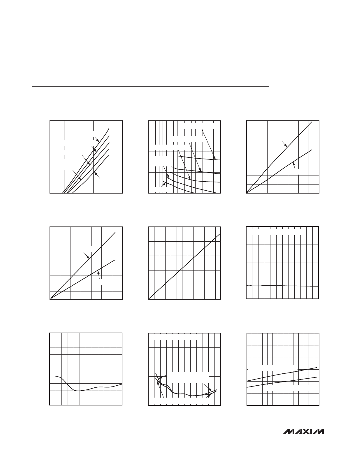
1.0625Gbps至11.3Gbps、
SFP+
双通道限幅放大器
典型工作特性(续
(VCC = 3.3V, TA = +25NC, unless otherwise noted. Registers are set to default values, unless otherwise noted, and the 3-wire interface
is static during measurements.)
DEEMPHASIS VALUE
DIFFERENTIAL OUTPUT SIGNAL LEVEL
vs. SET_CML DAC SETTING
1200
)
P-P
MAX3945
1100
1000
900
800
700
600
500
DIFFERENTIAL OUTPUT AMPLITUDE (mV
400
RXDE1 = 0, RXDE0 = 0
RXDE1 = 0, RXDE0 = 1
RXDE1 = 1,
RXDE0 = 0
50 300
RSSI MONITOR-BASED LOS THRESHOLDS
(LOS1_EN = 0 AND LOS2_EN = 1)
180
160
140
120
100
80
60
LOS THRESHOLD (mV)
40
20
0
0 70
RXDE_EN = 0
RXDE1 = 1,
RXDE0 = 1
SET_CML DAC SETTING
DEASSERT
ASSERT
SET_LOS[5:0] DAC CODE
vs. SET_CML DAC SETTING
(RATE_SEL = 1)
MAX3945 toc10
250200100 150
6
RXDE1 = 0, RXDE0 = 1
4
RXDE1 = 0,
RXDE0 = 0
2
DEEMPHASIS LEVEL (dB)
RXDE_EN = 0
0
50 250
RXDE1 = 1, RXDE0 = 1
RXDE1 = 1, RXDE0 = 0
SET_CML DAC SETTING
MAX3945 toc11
200150100
LOS MASKING TIME vs. DAC SETTING
5000
MAX3945 toc13
4000
3000
2000
MASKING TIME (µs)
1000
605030 402010
0
0
SET_LOSTIMER[6:0] DAC CODE
MAX3945 toc14
12010080604020
Rx INPUT-BASED LOS THRESHOLD vs. DAC
CODE (LOS1_EN = 1 AND LOS2_EN = 0)
160
140
)
120
P-P
100
80
60
LOS THRESHOLD (mV
40
20
0
0 70
DEASSERT
ASSERT
SET_LOS[5:0] DAC CODE
DETERMINISTIC JITTER vs. INPUT AMPLITUDE AT 1.25Gbps
(K28.5 PATTERN, 933MHz INPUT FILTER)
25
RATE_SEL = 0, BW1 = 0, BW2 = 0
20
15
DJ (ps)
10
5
0 1200
SIGNAL AMPLITUDE (mV
1000800600400200
)
P-P
)
MAX3945 toc12
605010 20 30 40
MAX3945 toc15
DETERMINISTIC JITTER AT 10.32Gbps
(PRBS7 PATTERN WITH 100 CIDs, RATE_SEL = 1)
10
9
8
7
6
5
DJ (ps)
4
3
2
1
0
0 1200
INPUT SIGNAL AMPLITUDE (mV
1000800200 400 600
)
P-P
MAX3945 toc16
DETERMINISTIC JITTER vs. DATA RATE
(INPUT = 100mV
25
K28.5 PATTERN, RATE_SEL = 1
20
15
DJ (ps)
10
5
0
0 12
DJ WITH 100mV
ON POWER SUPPLY
DJ WITH NO NOISE ON POWER SUPPLY
DATA RATE (Gbps)
P-P
P-P
NOISE
)
963
POWER-SUPPLY CURRENT vs. TEMPERATURE
(SET_CML[7:0] = 91d)
80
70
MAX3945 toc17
60
LOS2_EN = 0 AND LOS1_EN = 1
50
40
POWER-SUPPLY CURRENT (mA)
30
20
-40 100
LOS2_EN = 1 AND LOS1_EN = 0
TEMPERATURE (°C)
8 ______________________________________________________________________________________
MAX3945 toc18
806040200-20
Page 9

1.0625Gbps至11.3Gbps、
SCC11 (dB)
SFP+
双通道限幅放大器
典型工作特性(续
)
(VCC = 3.3V, TA = +25NC, unless otherwise noted. Registers are set to default values, unless otherwise noted, and the 3-wire interface
is static during measurements.)
INPUT RETURN GAIN (SDD11)
(INPUT POWER OF 0dBm, ENABLED)
0
-10
-20
SDD11 (dB)
-30
-40
0 100
FREQUENCY (GHz)
101
OUTPUT COMMON-MODE RETURN GAIN (SCC22)
(INPUT POWER OF 0dBm, ENABLED)
0
-10
-20
SCC22 (dB)
-30
-40
1 100
FREQUENCY (GHz)
OUTPUT RETURN GAIN (SDD22)
(INPUT POWER OF 0dBm, ENABLED)
0
MAX3945 toc19
-10
-20
SDD22 (dB)
-30
-40
0 100
FREQUENCY (GHz)
101
TRANSIENT RESPONSE (10.3Gbps,
10 ONES 10 ZEROS PATTERN, SET_CML[7:0] = 92d)
0.25
0.20
MAX3945 toc22
10
0.15
0.10
A = 1.39dB, RXDE1 = 0, RXDE0 = 0
B = 2.12dB, RXDE1 = 0, RXDE0 = 1
0.05
C = 3.27dB, RXDE1 = 1, RXDE0 = 0
0
D = 4.37dB, RXDE1 = 1, RXDE0 = 1
-0.05
-0.10
-0.15
-0.20
-0.25
0 1000
INPUT COMMON-MODE RETURN GAIN (SCC11)
(INPUT POWER OF 0dBm, ENABLED)
0
MAX3945 toc20
-10
-20
-30
-40
1 100
TIME (ps)
FREQUENCY (GHz)
A
C
B
D
800600400200
10
MAX3945 toc23
MAX3945 toc21
MAX3945
ELECTRICAL EYE DIAGRAM AFTER 6in OF FR4
AND 72in OF CABLE WITH NO DEEMPHASIS (11.3Gbps K28.5,
RATE_SEL = 1, SET_CML[7:0] = 160d, RXDE_EN = 0)
100mV/div
20ps/div
MAX3945 toc24
_______________________________________________________________________________________ 9
AND 72in OF CABLE WITH DEEMPHASIS (11.3Gbps K28.5, RATE_SEL = 1,
ELECTRICAL EYE DIAGRAM AFTER 6in OF FR4
SET_CML[7:0] = 160d, RXDE_EN = 1, RXDE0 = 1, RXDE1 = 1)
80mV/div
20ps/div
MAX3945 toc25
Page 10

1.0625Gbps至11.3Gbps、
SFP+
MAX3945
双通道限幅放大器
TOP VIEW
V
CCR
RIN-
RIN+
V
CCR
*THE EXPOSED PAD MUST BE CONNECTED TO GROUND.
RPMIN
12 10 9
13
14
15
16
+
1 3
CAZ
THIN QFN
(3mm × 3mm)
CSEL
11
MAX3945
2
EE
V
SDA
EE
V
*EP
引脚配置
SCL
V
8
CCR
ROUT-
7
ROUT+
6
V
5
CCR
4
LOS
引脚说明
引脚 名称 功能
1 CAZ
2, 3 V
4 LOS
5, 8, 13,
16
6 ROUT+
7 ROUT-
9 SCL
10 SDA
11 CSEL
12 RPMIN
14 RIN-
15 RIN+
— EP
V
EE
CCR
失调修正环路电容。连接在该引脚和相邻
AZ_EN=0
限幅放大器接地端。
信号丢失检测输出,该输出为漏极开路输出。当输入信号电平下降到
报警输出;当信号电平高于门限时,解除
LOS1_EN=0和LOS2_EN=0
电源,为限幅放大器提供供电电压。所有的引脚必须连接至供电电源。
同相输出,
反相输出,
串行时钟输入,
串行数据双向
电阻,以满足
片选输入,
并复位控制状态机。
高阻接收器功率监测输入。不使用时连接到地。
反相数据输入,
同相数据输入,
裸焊盘,必须焊接到电路地。
,并将该引脚连接至地,即可禁用失调修正。
,即可禁用
负载背向端接。
CML。50
CML。50
TTL/CMOS
Ω
负载背向端接。
Ω
TTL/CMOS
I/O,TTL/CMOS
线数字时序的要求(提供数据线冲突保护)。
3
。该引脚具有
输入和漏极开路输出。该引脚具有
。在内部由
75k
端接。
CML,50
CML,50
Ω
端接。
Ω
引脚之间的电容设置失调修正环路的时间常数。通过数字接口设置
V
EE
报警状态。设置
LOS
电路,参见表8。
LOS
内部下拉电阻。
Ω
75k
电阻下拉。
Ω
CSEL=1
LOS_POL=0
75k
启动一个
SET_LOS[5:0]
设置的门限以下时,触发
可以使
输出极性反转。通过设置
LOS
内部上拉电阻,但需要一个
Ω
工作周期;
SPI
CSEL=0
时,终止
4.7k
外部上拉
Ω
工作过程,
SPI
LOS
10 _____________________________________________________________________________________
Page 11

1.0625Gbps至11.3Gbps、
MAX3945
器件包 括一个双 通 道 限 幅 器、失调修正电 路、
级和
制。控制器件功能的寄存器包括 :
的设计工作 速 率为
电 路。
LOS
MAX3945
1.0625Gbps至11.3Gbps
的特性可 通 过 片上3线接口 控
RXCTRL1、RXCTRL2
详细说明
输出
CML
。
、
RXSTAT、SET_CML、SET_LOS、MODECTRL和SET_
LOSTIMER
控制器
限 幅 放 大 器 包 含 一 路 低 数 据 速 率 通 道
4.25Gbps)
对整体系统性能进行优化处理,图
通路选择由
可编程滤波器,在
4.25Gbps
数据率下的最佳接收灵敏度并降低最大接收带宽。表
表
1.
。
MAX3945
使用,图1所示为输入和输出结构的简化框图。
IC
和一路高数据速率通道(高达
RATE_SEL
1.0625Gbps、1.25Gbps、2.125Gbps
速率下优化工作性能。调整第一级带宽得到特定
数据速率选择和带宽控制
RXCTRL1[3:1] OPERATION MODE DESCRIPTION
BW1 BW0 RATE_SEL
0 0 0 1.0625 to 1.25 1000 52
0 1 0 2.125 2100 52
1 0 0 2.125 2500 52
1 1 0 4.25 3000 52
X X 1 11.3 9000 26
提供 集成
,允许配合低成 本
DAC
双通道限幅器
(1.0625Gbps
11.3Gbps)
所示为功能框图。数据
2
位控制。低数据速率通道还带有一个
至
,能够
和
汇总
1
DATA RATE
(Gbps)
SFP+
了
RATE_SEL、BW1和BW0
11.3Gbps
通过
性,如表
失调修正电路用于消除差分放大器固有的失调电压所产生的
PWD
修正环路的截止频率设置在大约
时,建议采用高数据速率模式
所示。
2
位设置
RX_POL
。连接 在
0.7kHz(RATE_SEL=1)
环路,如表
输出级优化于 差 分
CML
SQ_EN
所示。
3
位及内部
FILTER BANDWIDTH
双通道限幅放大器
控制位的功能,工作速率高达
(RATE_SEL=1)。
ROUT+/ROUT-
引脚和 地之间的
CAZ
。利用
100
状态组合控制,请参考表4。
LOS
(MHz)
相对于
0.1µF
2kHz(RATE_SEL=0)
AZ_EN
负载。输出 级 由
Ω
位可禁用失调修正
CML
RISE/FALL TIME
RIN+/RIN-
失调修正电路
外部电容将失调
输出使能和禁止
(ps)
CML
RX_EN
的极
或
输出级
和
MAX3945
表
信号极性控制 表
2.
RX_POL OPERATION MODE DESCRIPTION
0 Inversed polarity of the differential signal path
1 Normal polarity of the differential signal path
表
4. CML
输出级工作模式
RX_EN SQ_EN LOS STATUS OPERATION MODE DESCRIPTION
0 X X CML output disabled
1 0 X CML output enabled
1 1 0 CML output enabled
1 1 1 CML output disabled
______________________________________________________________________________________ 11
失调修正使能/禁止控制
3.
AZ_EN OPERATION MODE DESCRIPTION
0 Autozero loop is disabled
1 Autozero loop is enabled
Page 12

1.0625Gbps至11.3Gbps、
SFP+
MAX3945
双通道限幅放大器
V
CCR
RIN+
50Ω
V
- 1V
CCR
50Ω
RIN-
V
EER
LOS
376Ω
CLAMP
SDA
DEEMPHASIS
V
CCD
CONTROL
75kΩ
50Ω 50Ω
V
EER
SCL, CSEL
V
CCR
ROUT+
ROUT-
V
CCD
75kΩ
V
图
1.输入/
RPMIN
输出结构简化框图
EET
V
CCR
V
EER
2kΩ2kΩ
2pF
COMPARATOR
DAC
V
EER
12 _____________________________________________________________________________________
Page 13

1.0625Gbps至11.3Gbps、
RIN+
RIN-
RPMIN
V
CCR
SFP+
双通道限幅放大器
MAX3945
V
CCR
MAX3945
DIGITAL OFFSET CORRECTION
V
- 1V
CCR
R
IN
R
PULL
R
IN
BW1
LPF
BW0
4G
10G
CAZ
1
1
0
0
MX
RATE_SEL
LOSS OF SIGNAL
LOS_POL LOS2/1_EN
AZ_EN
RX_POL
RX_EN
SQ_EN
RXDE1
RXDE0
OUTPUT
CTRL LOGIC
R
OUT
DEEMPHASIS
V
CCR
R
OUT
ROUT+
ROUT-
LOS
SDA
SCL
CSEL
图
功能框图
2.
输出级针对标准
CML
化。
RXDE1和RXDE0
补偿
控制设置。
电路板损耗和
FR4
3-WIRE
R
PULL
FR4
R
PULL
电路板的
INTERFACE
CML
差分传输线进行优
100
Ω
INTERNAL
REGISTER
输出去加重
位增加了可编程模拟输出去加重,以
连接器损耗,表5给出了去加重
SFP
CONTROL
LOGIC
V
EE
8位SET_CML
电平取决于
平
假设采用理想的
(
所示为相应的输出
7
6b DAC SET_LOS
7b DAC SET_LOSTIMER
寄存器控制
MAX3945
100
DAC
8b DAC SET_CML
设置
输出幅度,最大可编程输出
CML
CML
输出幅度
的工作模式。表6列出了这些输出电
差分负载)及其相应的控制位,表
Ω
分辨率。
______________________________________________________________________________________ 13
Page 14

1.0625Gbps至11.3Gbps、
SFP+
表
5.
MAX3945
表
6. CML
双通道限幅放大器
输出信号去加重控制
RXCTRL2[1] RXCTRL1[7:6] OPERATION MODE DESCRIPTION
RXDE_EN RXDE1 RXDE0 MODE
0 X X Deemphasis block is disabled 0
1 0 0 Deemphasis block is enabled Level 1 0.3
1 0 1 Deemphasis block is enabled Level 2 1.1
1 1 0 Deemphasis block is enabled Level 3 2.1
1 1 1 Deemphasis block is enabled Level 4 4.3
输出幅度范围(典型值
RXCTRL1[1] RXCTRL2[1] RXCTRL1[7:6]
RATE_SEL RXDE_EN RXDE1 RXDE0
0 X X X Low data-rate path 400 to 1192
1 0 X X High data-rate path 400 to 1147
1 1 0 0 High data-rate path with deemphasis 400 to 1041
1 1 0 1 High data-rate path with deemphasis 400 to 987
1 1 1 0 High data-rate path with deemphasis 400 to 908
1 1 1 1 High data-rate path with deemphasis 400 to 828
)
MODE
DEEMPHASIS
(dB)
OUTPUT
AMPLITUDE
(mV
P-P
)
表
7. CML
RXCTRL1[1] RXCTRL2[1] RXCTRL1[7:6]
RATE_SEL RXDE_EN RXDE1 RXDE0
输出
0 X X X Low data-rate path 4.5
1 0 X X High data-rate path 4.5
1 1 0 0 High data-rate path with deemphasis 4.1
1 1 0 1 High data-rate path with deemphasis 3.9
1 1 1 0 High data-rate path with deemphasis 3.6
1 1 1 1 High data-rate path with deemphasis 3.3
分辨率(典型值
DAC
)
MODE
RESOLUTION
)
(mV
P-P
14 _____________________________________________________________________________________
Page 15

1.0625Gbps至11.3Gbps、
SFP+
表
8. LOS
LOS2_EN LOS1_EN OPERATION MODE DESCRIPTION
图
对短突发脉冲输入信号的
3.
控制
0 0 LOS circuitry is disabled and powered down
X 1 LOS circuitry is enabled and Rx input amplitude is detected
1 0 LOS circuitry is enabled and RPMIN input amplitude is detected
电路有两种工作模式,由
LOS
制
参见表8)。第一种模 式下,
50mV/div
2mV/div
50mV/div
2mV/div
LOS
400µs/div
响应
(
分幅度,并将其与
限进行比较 ;第二种模式下,
与
SET_LOS
二种模式根据平均光电二极管电流使能低功耗
触 发
LOS[5:0]
倍,避免
不受
这一功能能够在光纤链路发生光信号丢失事件后屏蔽故障输
入信号。这些故障输入信号由互阻放大器的工作所导致,可
能扰乱
LOS
设置在
跳变初始化输出屏蔽定时器,并在可编程
束之前避免对
输出屏蔽时间,使其大于任何预计的输入干扰的持续时间。
图
3
报 警 输 出 的 门 限 大 约 为
LOS
;解除
LOS
LOS1_EN或LOS2_EN
LOS
输出屏蔽时间可利用7位
0至4500µs
中未使用
800µs后,LOS
间功能,当输入信号发生变化时,
SET_LOS
寄存器的6个控制位预设的门限进 行比较。第
报警状态的门限大约为触发门限的
LOS
稠楸。
LOS
输出并导致系统级链路的诊断错误。
范围,步长为
输出信号的任何改变。应该仔细选择
LOS
输出屏蔽时间功能,当输入信号变化大约
LOS
信号发生变化。图4采用了
双通道限幅放大器
电路
LOS
LOS1_EN和LOS2_EN
电路检测输入信号的差
LOS
寄存器的6个控制位预设的门
电路将
LOS
RPMIN
LOS
1.5mV
极性、禁止控制以及
选择的影响。
可编程
P- P
LOS
输出屏蔽时间
LOS
SET_LOSTIMER[6:0]
35µs。LOS
信号的第1次
LOS
LOS
信号被屏蔽。
LOS
位控
引脚电压
检测。
xSET_
1.6
屏蔽时间
寄存器
屏蔽周期结
LOS
输出屏蔽时
MAX3945
对短突发脉冲输入信号的
图
4.
蔽
的任何变化
LOS
400µs/div
LOS响应(在LOS
)
______________________________________________________________________________________ 15
屏蔽周期结束之前屏
Page 16

1.0625Gbps至11.3Gbps、
SFP+
表
9.
15 14 13 12 11 10 9 8 7 6 5 4 3 2 1 0
表
10.
MAX3945
MAX3945
时钟。
CSEL
CSEL
开始产生时钟信号,所有的数据传输均为最高有效位
在前。
双通道限幅放大器
数字通信字结构
BIT
Register Address RWN Data that is written or read.
寄存器说明和地址
ADDRESS NAME FUNCTION
H0x00 RXCTRL1 Receiver Control Register 1
H0x01 RXCTRL2 Receiver Control Register 2
H0x02 RXSTAT Receiver Status Register
H0x03 SET_CML CML Output Level Setting Register
H0x04 SET_LOS LOS Threshold Assert Level Setting Register
H0x0E MODECTRL General Control Register
H0x12 SET_LOSTIMER LOS Timer Setting Register
线数字通信
3
概述
采用 专有 的3线数字 接口,由外部 控制器产生
线接口由
3
片选输入(高电平有效)组成。外部主控制器通过使能
引脚启动一次数据传输。主控制器在
双向 数 据线、
SDA
时钟信号 输入和
SCL
CSEL
引脚置1后
(MSB)
通过将
了不同的时序参数。
主控制器在
沿向
SDA
位之 后 释 放
在前)。主控制器通过将
(MSB
为接口时序。
CSEL置0
终止传输。图5所示为接口时序,表11定义
SCL产生16
输出数据,共计8位数据
,从器件在时钟的上升沿输 出8位 数 据
SDA
读模式
个时钟周期。主控制器在时钟下降
(MSB在前)
CSEL置0
终止传输,图5所示
(RWN = 1)
。发 送
RWN
协议
每次操作包括16位传输
主控制器向
传输8位数据。
参考表
MAX3945有7
主控制器在
沿向
16 _____________________________________________________________________________________
SCL发出16
RWN
9。
个可编程寄存器,表10列出了寄存器及其地址。
SCL产生16
输出数据,共计16位数据
SDA
位地址/数据、1位
(15
个时钟周期,所有操作向
位确定周期为读 操作 还是写操作,请
写模式
个时钟周期。主控制器在时钟下降
(MSB在前)
。总线
RWN)
MAX3945
寄存器地址
(RWN = 0)
。主控制器
常规模式下允许对
命令,默认模式为常规模式。
设 置模 式 下允许主控制器对
进 行 写 操 作, 写入 数 据 不 受 限 制。为了进 入 设 置 模 式,
MODECTRL
MODECTRL
下一步操作完成之后,自动退出设置模式状态。如果需要进
行多次不受限的设置,必须重复这一过程。
MODECTRL
寄 存 器(地 址
寄存器置为
以外的所有寄存器执行只读
RXSTAT
=H0x0 E)
后,随后操作不再受限。在
H0x12
模式控制
以外的所有寄存 器
必 须 置 为
H0x12
。
Page 17

1.0625Gbps至11.3Gbps、
图
表
CSEL
SDA
CSEL
SDA
5.3
11.
WRITE MODE
t
L
tCHt
CL
SCL
READ MODE
t
SCL
线数字接口时序
L
A6 A5 A4 A3 A2 A1 A0
1 2 3 4 5 6 7 8A69 10 11 12 13 14 150
t
DS
A5 A4 A3 A2 A1 RWN D7 D6 D5 D4 D3 D2 D1 D0
t
DH
tCHt
CL
1 2 3 4 5 6 7 8 9 10 11 12 13 14 150
t
DS
t
DH
A0
D7 D6 D5 D4 D3 D2 D1 D0RWN
接口时序参数
SYMBOL DEFINITION
CSEL leading time before the first SCL edge
SCL pulse-width high
SCL pulse-width low
SCL rise to SDA propagation time
SDA setup time
SDA hold time
CSEL trailing time after last SCL edge
t
t
t
CH
t
CL
t
DS
DH
t
L
D
t
T
SFP+
t
D
双通道限幅放大器
t
T
t
T
MAX3945
接收器控制寄存器
Bit #
Name RXDE1 RXDE0 X* SOFTRES BW1 BW0 RATE_SEL X*
Default Value 0 0 1 0 1 1 1 1
第7位和第6位:
第4位:
SOFTRES
第3位和第2位:
第1位:
RATE_SEL
RATE_SEL置1
7 6 5 4 3 2 1 0 ADDRESS
请勿修改默认设置。
*
RXDE[1:0]
。在3线接口写操作期间,若将该位置1,一旦
BW[1:0]
时,选择宽带通路;
______________________________________________________________________________________ 17
。这2位用于控制输出波形去加重,关于控制位设置及相应的去加重电平,请参考表5。
变为低电平,所有寄存器将置为默认状态。
CSEL
。
RATE_SEL=0
。
RATE_SEL
选择窄带数据通路
RATE_SEL置0
时,这2位控制限幅放大器带宽,相关设置及滤波器选择请参考表1。
(1.0625Gbps至4.25Gbps)
和宽带数据通 路
(4.25Gbps至11.3Gbps)
时,选择窄带通路。
寄存器说明
1 (RXCTRL1)
H0x00
。
Page 18

1.0625Gbps至11.3Gbps、
SFP+
Bit #
Name LOS2_EN LOS1_EN LOS_POL RX_POL SQ_EN RX_EN RXDE_EN AZ_EN
Default Value 0 1 1 1 0 1 0 1
第7位:
基于
MAX3945
LOS2_EN LOS1_EN RX_EN Rx INPUT-BASED LOS RSSI MONITOR-BASED LOS
第
6位:LOS1_EN
0=
1=
第5位:
0=
1=
第4位:
0=
1=
第
3位:SQ_EN
0=
1=
第2位:
0=
1=
第1位:
0=
1=
第0位:
0=
1=
双通道限幅放大器
接收器控制寄存器
7 6 5 4 3 2 1 0 ADDRESS
LOS2_EN
监测器的
RSSI
0 0 X Disabled and powered down Disabled and powered down
0 1 1 Enabled Disabled and powered down
X 1 0 Disabled and powered down Disabled and powered down
1 1 1 Enabled Disabled and powered down
1 0 0 Disabled and powered down Enabled
1 0 1 Disabled and powered down Enabled
禁止
使能
LOS_POL
反相
标称极性
RX_POL
反相
标称极性
禁止
使能
RX_EN
禁止
使能
RXDE_EN
禁止
使能
AZ_EN
禁止
使能
。使能或禁用基于
。
LOS
。控制基于Rx输入的
。控制
引脚极性。
LOS
。控制
CML
输出极性。
。
SQ_EN=1时,CML
。使能或禁用接收电路。
。使能或禁用
CML
。使能或禁用自动调零电路。
监测器的
RSSI
电路,
LOS
输出在触发
输出去加重。
电路,与
LOS
RX_EN置0
报警时被禁止。
LOS
LOS1_EN
时也禁止
位组合控制。下表列出了什么情况下禁用或使能
检测电路。
LOS
2 (RXCTRL2)
H0x01
18 _____________________________________________________________________________________
Page 19

1.0625Gbps至11.3Gbps、
SFP+
Bit #
Name X X X X X X POR_2d LOS_2d
Default Value X X X X X X X X
第1位:
路的报警状态,但
第0位:
该位或发生
第7位至第0位:
CML
POR_2d
LOS_2d
POR
Bit #
Name
Default Value 0 1 0 1 1 1 0 0
输出电平和
Bit #
Name X X
Default Value X X 0 0 1 1 0 0
7 6 5 4 3 2
。当
。
。
SET_CML[7]
SET_CML[7:0]
SET_CML
供电电压低于
V
CC
POR_2d
LOS
(MSB)
位仍将保持高电平,直到读取该位。
状态的拷贝。这是一个关联位,读操作后清除。锁存第一次逻辑0至逻辑1的变化,直到主控制器读取
7 6 5 4 3 2 1 0 ADDRESS
SET_CML[6] SET_CML[5] SET_CML[4] SET_CML[3] SET_CML[2] SET_CML[1]
之间关系的公式请参考表13。
7 6 5 4 3 2 1 0 ADDRESS
2.3V时,POR
。
SET_CML
寄存器为8位寄存器,最大可置为
SET_LOS[5]
(MSB)
电路将
POR_2d
置为高电平;当供电电压高于
SET_LOS[4] SET_LOS[3] SET_LOS[2] SET_LOS[1]
双通道限幅放大器
接收器状态寄存器
1
(STICKY)0 (STICKY)
2.75V
输出电平设置寄存器
CML
SET_CML[0]
(LSB)
,对应于最大
255
门限触发电平设置寄存器
LOS
输出幅度。关于确定
CML
SET_LOS[0]
(LSB)
(RXSTAT)
ADDRESS
H0x02
时,将解除
(SET_CML)
H0x03
(SET_LOS)
H0x04
POR
MAX3945
电
第5位至第0位:
监测器的
LOS
的典型
SET_LOS[5:0]
LOS
______________________________________________________________________________________ 19
。
SET_LOS
门限电压与
DAC
寄存器为6位寄存器,用于设置
码之间的关系,请参考
典型工作特性
门限。关于基于Rx输入的
LOS
部分。
LOS
和基于
RSSI
Page 20

1.0625Gbps至11.3Gbps、
SFP+
双通道限幅放大器
通用控制寄存器
Bit #
Name
Default
Value
7 6 5 4 3 2 1 0 ADDRESS
MODECTRL[7]
(MSB)
0 0 0 0 0 0 0 0
MODECTRL[6] MODECTRL[5] MODECTRL[4] MODECTRL[3] MODECTRL[2] MODECTRL[1]
MAX3945
第7位至第0位:
择设置模式状态。
Bit #
Name X
Default Value X 0 0 0 0 0 0 0
第6位至第0位:
码之间的关系,请参考
DAC
表
12.
寄存器
MODECTRL[7:0]
MODECTRL
7 6 5 4 3 2 1 0 ADDRESS
SET_LOSTIMER[6:0]
。
MODECTRL
寄存器使能常规模式和设置模式之间的转换。将该寄存器置为
必须在每次写操作之前更新。
SET_
LOSTIMER[6]
(MSB)
典型工作特性
SET_
LOSTIMER[5]
。
SET_LOSTIMER
部分。
SET_
LOSTIMER[4]
SET_
LOSTIMER[3]
SET_
LOSTIMER[2]
寄存器为7位寄存 器,数值 范围从0至
定时器设置寄存器
LOS
SET_
LOSTIMER[1]
MODECTRL[0]
(LSB)
(SET_LOSTIMER)
SET_
LOSTIMER[0]
(LSB)
关于定时器周期与
127。
(MODECTRL)
H0x0E
时,选
H0x12
H0x12
REGISTER
FUNCTION/
ADDRESS
Receiver
Control
Register 1
Address =
H0x00
REGISTER
NAME
RXCTRL1
NORMAL
MODE
R RW 7 RXDE1 0
R RW 6 RXDE0 0
R RW 5 X 1 Must be set to 1
R RW 4 SOFTRES 0
R RW 3 BW1 1
R RW 2 BW0 1
R RW 1 RATE_SEL 1
R RW 0 X 1 Must be set to 1
SETUP
MODE
BIT NUMBER/
TYPE
BIT NAME
DEFAULT
VALUE
NOTES
Rx deemphasis
MSB control with
RXDE_EN = 1
Rx deemphasis
LSB control with
RXDE_EN = 1
Soft reset control
bit
Input bandwidth
control with
RATE_SEL = 0:
00: 1GHz
01: 2.1GHz
10: 2.5GHz
11: 3GHz
Rate-select control
0: 1G/4G mode
1: fast mode
20 _____________________________________________________________________________________
Page 21
1.0625Gbps至11.3Gbps、
表
寄存器(续
12.
REGISTER
FUNCTION/
ADDRESS
Receiver
Control
Register 2
Address =
H0x01
)
REGISTER
NAME
RXCTRL2
SFP+
NORMAL
MODE
R RW 7 LOS2_EN 0
R RW 6 LOS1_EN 1
R RW 5 LOS_POL 1
R RW 4 RX_POL 1
R RW 3 SQ_EN 0
R RW 2 RX_EN 1
R RW 1 RXDE_EN 0
SETUP
MODE
BIT NUMBER/
TYPE
BIT NAME
双通道限幅放大器
DEFAULT
VALUE
MAX3945
NOTES
RSSI monitorbased LOS
0: disabled
1: enabled when
LOS1_EN = 0
Rx input-based
LOS
0: disabled
1: enabled
LOS polarity
0: inverse
1: normal
Rx polarity
0: inverse
1: normal
Squelch
0: disabled
1: enabled
Rx control
0: disabled
1: enabled
Rx deemphasis
0: disabled
1: enabled
Receiver
Status
Register
Address =
H0x02
Rx autozero
R RW 0 AZ_EN 1
R R 1 (sticky) POR_2d X
RXSTAT
R R 0 (sticky) LOS_2d X
______________________________________________________________________________________ 21
control
0: disabled
1: enabled
POR -> V
limit violation
Copy of LOS
status
CC
low
Page 22
1.0625Gbps至11.3Gbps、
SFP+
表
12.
REGISTER
FUNCTION/
ADDRESS
MAX3945
CML Output
Level
Setting
Register
Address =
H0x03
LOS
Threshold
Assert Level
Setting
Register
Address =
H0x04
General
Control
Register
Address =
H0x0E
LOS Timer
Setting
Register
Address =
H0x12
双通道限幅放大器
寄存器(续
)
REGISTER
NAME
SET_CML
SET_LOS
MODECTRL
SET_LOSTIMER
NORMAL
MODE
R RW 7 SET_CML[7] 0
R RW 6 SET_CML[6] 1
R RW 5 SET_CML[5] 0
R RW 4 SET_CML[4] 1
R RW 3 SET_CML[3] 1
R RW 2 SET_CML[2] 1
R RW 1 SET_CML[1] 0
R RW 0 SET_CML[0] 0
R RW 5 SET_LOS[5] 0
R RW 4 SET_LOS[4] 0
R RW 3 SET_LOS[3] 1
R RW 2 SET_LOS[2] 1
R RW 1 SET_LOS[1] 0
R RW 0 SET_LOS[0] 0
RW RW 7 MODECTRL[7] 0
RW RW 6 MODECTRL[6] 0
RW RW 5 MODECTRL[5] 0
RW RW 4 MODECTRL[4] 0
RW RW 3 MODECTRL[3] 0
RW RW 2 MODECTRL[2] 0
RW RW 1 MODECTRL[1] 0
RW RW 0 MODECTRL[0] 0
R RW 6 SET_LOSTIMER[6] 0
R RW 5 SET_LOSTIMER[5] 0
R RW 4 SET_LOSTIMER[4] 0
R RW 3 SET_LOSTIMER[3] 0
R RW 2 SET_LOSTIMER[2] 0
R RW 1 SET_LOSTIMER[1] 0
R RW 0 SET_LOSTIMER[0] 0
SETUP
MODE
BIT NUMBER/
TYPE
BIT NAME
DEFAULT
VALUE
NOTES
MSB output level
DAC
LSB output level
DAC
MSB LOS threshold DAC
LSB LOS threshold DAC
MSB mode control
LSB mode control
MSB LOS timer
LSB LOS timer
22 _____________________________________________________________________________________
Page 23

1.0625Gbps至11.3Gbps、
设置
CML
请参考表13和表14,对于表13中
个值,去加重值随着
出了
SET_CML[7:0]=120d
CML[7:0]
请参 考
(
设置情况下的去 加重值, 请 参 考
DeemphasisValuevs.SET_CMLDACSetting
(RATE_SEL=1)
幅值控制低于
仍然会存在一定程度的去加重。
对于交流耦合,耦合电容
确定性抖动降至最小。当输入低频截点
减小 :
fIN=1/[2π(50)(CIN)]
用
0.1µF的C
表
13. CML
RXCTRL1[1] RXCTRL2[1] RXCTRL1[7:6]
RATE_SEL RXDE_EN RXDE1 RXDE0
IN
0 X X X 0 45mV
1 0 X X 0.72 4.5mV
1 1 0 0 1.17 -4mV
1 1 0 1 1.89 -7mV
1 1 1 0 2.48 -10mV
1 1 1 1 3.86 -13mV
SET_CML[7:0]
曲线图)。注意,即使
SET_CML[7:0]=170d且RATE_SEL=1
C
C
OUT
。
和
输出幅度公式(典型值
RXDE1和RXDE0
的设置而变化。表13给
情况下的去加重值,其它
典型工作特性
RXDE_EN=0
选择耦合电容
和
IN
。建议在
的选 择应使 接收器的
C
OUT
降低时,抖动会
(fIN)
MAX3945
)
设计步骤
输出电平
位的每
SET_
,当
应用中采
和地之间的电 容决定了信号通路直 流 失调 抑 制环路
CAZ
的时间常数,建议在
电容。
采用良好的高频布线技术以及不间断地平面的多层电路板,
将
和串扰降至最小。
时,
(SET_CML[7:0] = 120d)
EMI
16引脚TQFN
道。该 焊盘也是
的地,以保证适当的散热和电气性能。详细信息请参考应用
笔记
862
:
andOtherExposed-PaddlePackages
DEEMPHASIS (dB)
SFP+
双通道限幅放大器
选择失调修正电容
MAX3945的CAZ
和地之间采用
应用信息
0.1µF
布局考虑
裸焊盘封装
封装的裸焊盘为IC提供了一条低热阻散 热通
MAX3945
的电气 地, 必须焊 接到电路板
HFAN-08.1:ThermalConsiderationsofQFN
。
EQUATION FOR (V
+ 4.5mV
P-P
x SET_CML
P-P
+ 4.1mV
P-P
+ 3.9mV
P-P
+ 3.6mV
P-P
+ 3.3mV
P-P
P-P
P-P
P-P
P-P
P-P
- V
ROUT+
x SET_CML
x SET_CML
x SET_CML
x SET_CML
x SET_CML
ROUT-
)
MAX3945
表
14. 400mV
RXCTRL1[1] RXCTRL2[1] RXCTRL1[7:6] SET_CML DAC CODE
RATE_SEL RXDE_EN RXDE1 RXDE0 400mV
0 X X X 80 169
1 0 X X 91 181
1 1 0 0 98 194
1 1 0 1 106 208
1 1 1 0 115 225
1 1 1 1 126 245
和
P-P
800mV
______________________________________________________________________________________ 23
输出电平的
P-P
SET_CML DAC
编码
P-P
800mV
P-P
Page 24

1.0625Gbps至11.3Gbps、
SFP+
MAX3945
双通道限幅放大器
SFP+ OPTICAL RECEIVER
+3.3V
C
IN
0.1µF
0.1µF
I
R
RPMIN
RPMIN
100pF
2kΩ
10G PIN
FLEX ROSA
EP CAZ
V
V
RIN+
RIN-
RPMIN
SCL
SDA
CSEL
EE
CCR
MAX3945
11.3Gbps
3-WIRE
INTERFACE
POWER-ON RESET
SUPPLY
FILTER
0.1µF
LOS
ROUT+
ROUT-
0.1µF
C
OUT
0.1µF
SFP
CONNECTOR
HOST BOARD
FILTER
VCC_RX
+3.3V
= 100Ω
Z
DIFF
典型应用电路
HOST
4.7kΩ
SerDes
3-WIRE
INTERFACE
ADC
如需最 近 的 封 装 外形信 息和焊盘 布局, 请 查 询
状态。封装图中可能包含不同的尾缀字符,但封装图只与封装有关,与
封装类型 封装编码 文档编号
16 TQFN-EP T1633+5
Maxim
北京
免费电话:
电话:
传真:
Maxim不对Maxim
北京办事处
8328信箱
010-6211 5199
010-6211 5299
邮政编码
800 810 0310
100083
产品以外的任何电路使用负责,也不提供其专利许可。
china.maxim-ic.com/packages
Maxim
SFP+
CONTROLLER
RoHS
2
C
I
。请注 意,封 装 编 码中的“+”、“#”或“-”仅表 示
状态无关。
MODE_DEF2 (SDA)
MODE_DEF1 (SCL)
RATE SELECT
21-0136
保留在任何时间、没有任何通报的前提下修改产品资料和规格的权利。
封装信息
RoHS
24 Maxim Integrated Products, 120 San Gabriel Drive, Sunnyvale, CA 94086 408-737-7600
©
2010MaximIntegratedProducts Maxim是MaximIntegratedProducts,Inc.
的注册商标。
 Loading...