

Page 1
General Description
The MAX3892 serializer is ideal for converting 4-bitwide, 622Mbps parallel data to 2.5Gbps serial data in
DWDM and SONET/SDH applications. A 4
✕
4-bit FIFO
allows for any static delay between the parallel output
clock and parallel input clock. Delay variation up to a
unit interval (UI) is allowed after reset. A fully integrated
phase-locked loop (PLL) synthesizes an internal
2.5GHz serial clock from a 622MHz, 155.5MHz,
77.8MHz, or 38.9MHz reference clock. A selectable
dual VCO allows excellent jitter performance at both
SONET and forward-error correction (FEC) data rates.
Operating from a single 3.3V supply, this device
accepts low-voltage differential-signal (LVDS) clock and
data inputs for interfacing with high-speed digital circuitry, and delivers current-mode logic (CML) serial data
and clock outputs. A loopback data output is provided
to facilitate system diagnostic testing. The MAX3892 is
available in the extended temperature range (-40°C to
+85°C) in 44-pin QFN and TQFN packages.
Applications
SONET/SDH OC-48 Transmission Systems
WDM Transponders
Add/Drop Multiplexers
Dense Digital Cross-Connects
Backplane Interconnects
Features
♦ Single +3.3V Supply
♦ 455mW Power Consumption
♦ 1.4ps
RMS
Maximum Jitter Generation
♦ 4 ✕ 4-Bit FIFO Input Buffer
♦ 622Mbps/666Mbps Parallel to 2.5Gbps/2.7Gbps
Serial Conversion
♦ 622MHz/667MHz or 311MHz/333MHz Clock Input
♦ On-Chip Clock Synthesizer
♦ Multiple Clock Reference Frequencies:
(622.08MHz, 155.52MHz, 77.76MHz, 38.88MHz) or
(666.51MHz, 166.63MHz, 83.31MHz, 41.66MHz)
♦ LVDS Parallel Clock and Data Inputs
♦ CML Serial Data and Clock Outputs
♦ Additional CML Output for System Loopback
Testing
MAX3892
+3.3V, 2.5Gbps/2.7Gbps, SDH/SONET 4:1
Serializer with Clock Synthesis
________________________________________________________________
Maxim Integrated Products
1
Ordering Information
19-2215; Rev 6; 10/07
EVALUATION KIT
AVAILABLE
For pricing, delivery, and ordering information, please contact Maxim Direct at 1-888-629-4642,
or visit Maxim’s website at www.maxim-ic.com.
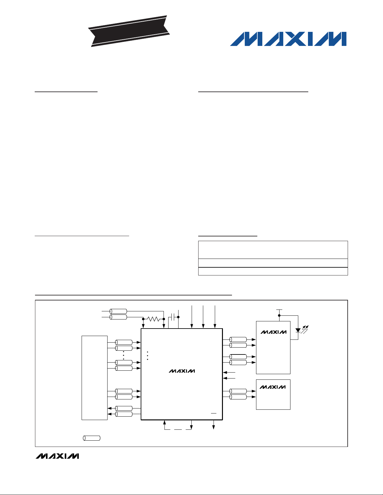
Typical Application Circuit
+
Denotes a lead-free package.
PART
MAX389 2EGH
MAX389 2ETH+
TEMP
RANGE
-40°C to +85° C
-40°C to +85° C
PINPACKAGE
PKG
CODE
44 QFN G4477-3
44 TQFN T4477-3
V
CC
MAX3273
LASER
DRIVER
MAX3882
1:4 DESERIALIZER
WITH CDR
RCLK+
RESET
= 50Ω.
O
C
FIL
VCCVCO
Z
VCCVCO
MAX3892
MODE
RATESET
SCLKO+
SCLKO-
SLBEN
SLBPD
SLBO+
SLBO-
CLKSET
FIFOERROR LOL
SDO+
SDO-
CML
CML
TTL
CML
OPTIONAL
FOR
SYSTEM
LOOPBACK
TEST
LVPECL
LVDS
SONET/SDH
FRAMER
LVDS
LVDS
THIS SYMBOL REPRESENTS A TRANSMISSION
LINE OF CHARACTERISTIC IMPEDANCE Z
100Ω
RCLK-
PDI0+
PDI0-
PDI3+
PDI3-
PCLKI+
PCLKI-
PCLKO+
PCLKO-
Page 2
MAX3892
+3.3V, 2.5Gbps/2.7Gbps, SDH/SONET 4:1
Serializer with Clock Synthesis
2 _______________________________________________________________________________________
ABSOLUTE MAXIMUM RATINGS
DC ELECTRICAL CHARACTERISTICS
(VCC= +3.0V to +3.6V, TA= -40°C to +85°C. Typical values are at VCC= +3.3V, differential LVDS load = 100Ω ±1%, TA= +25°C,
unless otherwise noted.) (Note 1)
Stresses beyond those listed under “Absolute Maximum Ratings” may cause permanent damage to the device. These are stress ratings only, and functional
operation of the device at these or any other conditions beyond those indicated in the operational sections of the specifications is not implied. Exposure to
absolute maximum rating conditions for extended periods may affect device reliability.
Supply Voltage VCC, VCCO, VCCVCO .....................-0.5V to +5V
All Inputs and FIL .......................................-0.5V to (V
CC
+ 0.5V)
LVDS Output Voltage (PCLKO±)................-0.5V to (V
CC
+ 0.5V)
CML Output Current (SDO±, SCLKO±, SLBO±) ................22mA
Continuous Power Dissipation (T
A
= +85°C)
44-Pin QFN (derate 25mW/°C above +85°C) ............1625mW
Operating Temperature Range ...........................-40°C to +85°C
Storage Temperature Range .............................-55°C to +150°C
Lead Temperature (soldering, 10s) .................................+300°C
Supply Current I
LVDS INPUT SPECIFICATIONS (PDI[3..0]±, PCLKI±)
Input Voltage Range V
Differential Input Voltage |VID| 100 mV
Input Common-Mode Current LVDS input VOS = 1.2V 61 µA
Threshold Hysteresis 45 mV
Differential Input Resistance R
LVPECL INPUT SPECIFICATIONS (RCLK±)
Input High Voltage V
Input Low Voltage V
Input Bias Voltage VCC - 1.3 V
Single-Ended Input Resistance >1.0 kΩ
Differential Input Voltage Swing 300 1900 mV
LVDS OUTPUT SPECIFICATIONS (PCLKO±)
Output High Voltage V
Output Low Voltage V
Differential Output Voltage |VOD| 250 400 mV
Change in Magnitude of
Differential Output Voltage for
Complementary States
Offset Output Voltage 1.125 1.275 V
Change in Magnitude of Output
Offset Voltage for Complementary
States
PARAMETER SYMBOL CONDITIONS MIN TYP MAX UNITS
CC
Δ|V
Δ|V
(Note 2) 138 190 mA
I
IN
IH
IL
OH
OL
| 25 mV
OD
| 25 mV
OS
0 2400 mV
83 100 117 Ω
VCC -
1.16
VCC -
1.81
0.925 V
VCC -
0.88
VCC -
1.48
1.475 V
V
V
P-P
Page 3
MAX3892
+3.3V, 2.5Gbps/2.7Gbps, SDH/SONET 4:1
Serializer with Clock Synthesis
_______________________________________________________________________________________ 3
AC ELECTRICAL CHARACTERISTICS
(VCC= +3.0V to +3.6V, TA= -40°C to +85°C. Typical values are at VCC= +3.3V, differential LVDS loads = 100Ω ±1%, CML loads =
50Ω ±1%, T
A
= +25°C, unless otherwise noted.) (Note 3)
DC ELECTRICAL CHARACTERISTICS (continued)
(VCC= +3.0V to +3.6V, TA= -40°C to +85°C. Typical values are at VCC= +3.3V, differential LVDS load = 100Ω ±1%, TA= +25°C,
unless otherwise noted.) (Note 1)
Differential Output Resistance 80 140 Ω
Output Current Shorted together 12 mA
Output Current Shorted to ground 40 mA
CML OUTPUT SPECIFICATIONS (SDO±, SCLKO±, SLBO±)
Differential Output RL = 100Ω differential 640 800 1000 mV
Differential Output Resistance 83 100 117 Ω
Output Common-Mode Voltage RL = 50Ω to V
LVTTL SPECIFICATIONS (RESET, RATESET, SLBEN, SLBPD FIFOERROR, LOL)
Input High Voltage V
Input Low Voltage V
Input High Current I
Input Low Current I
Output High Voltage V
Output Low Voltage V
PROGRAMMING INPUTS (CLKSET, MODE)
Input Current Input = 0 or V
PARAMETER SYMBOL CONDITIONS MIN TYP MAX UNITS
P-P
CC
IH
IL
IH
IL
IOH = 20µA 2.4 V
OH
IOL = 1mA 0.4 V
OL
CC
VCC - 0.2 V
2.0 V
0.8 V
-30 +10 µA
-50 +10 µA
CC
-500 +500 µA
V
PARALLEL INPUT SPECIFICATIONS (PDI±, PCLKI±)
Parallel Input Data Rate
Parallel Input Clock Rate
Parallel Input Setup Time t
Parallel Input Hold Time t
PARALLEL CLOCK OUTPUT SPECIFICATIONS (PCLKO±)
Parallel Clock Output Rise/Fall
Time
Parallel Clock Output Duty Cycle 46 54 %
SERIAL OUTPUT SPECIFICATIONS (SDO±, SCLKO±)
Serial Output Data Rate
Serial Data Output Rise/Fall Time tr, t
Serial Output Clock to Data Delay t
PARAMETER SYMBOL CONDITIONS MIN TYP MAX UNITS
SU
H
, t
t
r
CLK-Q
RATESET = GND 622
RATESET = V
MODE = OPEN or V
MODE = SHORT or 30kΩ to GND 311
(Note 4) -94 ps
(Note 4) 300 ps
20% to 80% 100 200 ps
f
RATESET = GND 2.488
RATESET = V
20% to 80% 80 ps
f
(Note 5) -25 25 ps
CC
CC
CC
666
622
2.666
Mbps
MHz
Gbps
Page 4
MAX3892
+3.3V, 2.5Gbps/2.7Gbps, SDH/SONET 4:1
Serializer with Clock Synthesis
4 _______________________________________________________________________________________
Note 1: Specifications at -40°C are guaranteed by design and characterization.
Note 2: Measured with SLBO/CLK622 and SCLK outputs disabled and CML outputs open.
Note 3: AC characteristics are guaranteed by design and characterization.
Note 4: In 622MHz clock mode, the parallel data is clocked in by the rising edge of the 622MHz/666MHz parallel clock input. In the
311MHz clock mode, the parallel data is clocked in on both the rising and falling edges of the clock. The parallel input
setup and hold time increases by 60ps if the duty cycle is between 48% to 52% in 311MHz mode (Figure 1).
Note 5: Relative to the falling edge of the SCLKO.
Note 6: Measurement bandwidth is BW = 12kHz to 20MHz.
Note 7: Measured with 00001111 pattern, RCLK to PCLKI/PDI[3:0] phase approximately 40ps. See the
Jitter Generation vs. RCLK to
PCLK/PDI[3:0] Phase
plot in the
Typical Operating Characteristics
section.
Note 8: Deterministic jitter includes pattern-dependent jitter and pulse-width distortion. Measured using a 2
7
- 1 PRBS pattern with
96 consecutive identical digits.
AC ELECTRICAL CHARACTERISTICS (continued)
(VCC= +3.0V to +3.6V, TA= -40°C to +85°C. Typical values are at VCC= +3.3V, differential LVDS loads = 100Ω ±1%, CML loads =
50Ω ±1%, T
A
= +25°C, unless otherwise noted.) (Note 3)
Serial Clock Output Jitter
Generation
Serial Data Output Random Jitter RJ (Note 7) 1.4 ps
Serial Data Output Deterministic
Jitter
REFERENCE CLOCK INPUT SPECIFICATIONS (RCLK)
Reference Clock Frequency
Tolerance
Reference Clock Input Duty Cycle 30 70 %
RESET INPUTS (RESET)
Minimum Pulse Width of FIFO
Reset
Tolerated Drift Between PCLKI
and PCLKO After Reset
PARAMETER SYMBOL CONDITIONS MIN TYP MAX UNITS
JG (Notes 6 and 7) 1.0 1.4 ps
DJ (Note 8) 19 ps
±100 ppm
UI is PCLKO period 4 UI
UI is PCLKO period ±1UI
RMS
RMS
P-P
Page 5

MAX3892
+3.3V, 2.5Gbps/2.7Gbps, SDH/SONET 4:1
Serializer with Clock Synthesis
_______________________________________________________________________________________
5
Typical Operating Characteristics
(VCC= +3.3V, CML loads AC-coupled to 50Ω ±1%, TA= +25°C, unless otherwise noted.)
Pin Description
SUPPLY CURRENT vs. TEMPERATURE
170
165
160
155
150
145
140
135
SUPPLY CURRENT (mA)
130
125
120
-40 -20 0 20 40 60 80 100
TEMPERATURE (°C)
JITTER GENERATION vs. POWER SUPPLY
NOISE AMPLITUDE (BW = 2MHz)
5.0
4.5
)
4.0
RMS
3.5
3.0
2.5
2.0
1.5
JITTER GENERATION (ps
1.0
0.5
0
0 10050 150 200 250
NOISE AMPLITUDE (V
P-P
MAX3892 toc01
1.4
1.2
MAX3892 toc04
)
RMS
1.0
0.8
0.6
0.4
JITTER GENERATION (ps
0.2
)
ELECTRICAL EYE DIAGRAM
PATTERN 213-1 PRBS
DATA RATE = 2.5Gbps
50ps/div
MAX3892 toc02
JITTER GENERATION
vs. RCLK to PCLKI/PDI[3:0] PHASE
PATTERN = 00001111
0
0 400
RCLK TO PCLKI/PDI[3:0] PHASE (ps)
35030025020015010050
MAX3892 toc05
POWER-SUPPLY JITTER GENERATION
vs. RIPPLE FREQUENCY
40
35
)
P-P
30
25
20
15
JITTER GENERATION (ps
10
5
0
10 1k 10k
100mV
P-P
50mV
P-P
100
RIPPLE FREQUENCY (kHz)
SERIAL-DATA OUTPUT JITTER
f
= 622MHz
RCLK
TOTAL WIDEBAND RMS JITTER = 1.3ps
PEAK-TO-PEAK JITTER = 15.8ps
5ps/div
MAX3892 toc03
MAX3892 toc06
PIN NAME FUNCTION
1, 16, 22, 27,
33, 44
2, 5, 8, 11 VCCO
GND Supply Ground
Supply Voltage for Outputs +3.3V. Add bypass capacitors near these pins before connecting to
the V
power plane.
CC
3 SCLKO- Negative Serial Clock Output, CML 2.488GHz or 2.666GHz
4 SCLKO+ Positive Serial Clock Output, CML 2.488GHz or 2.666GHz
6 SDO- Negative Serial Data Output, CML 2.488Gbps or 2.666Gbps
7 SDO+ Positive Serial Data Output, CML 2.488Gbps or 2.666Gbps
Page 6

MAX3892
+3.3V, 2.5Gbps/2.7Gbps, SDH/SONET 4:1
Serializer with Clock Synthesis
6 _______________________________________________________________________________________
Pin Description (continued)
PIN NAME FUNCTION
9 SLBO-
10 SLBO+
12 SLBPD
13 SLBEN
14 RESET
15 FIFOERROR
17, 28, 36, 43 V
18 LOL
19 MODE
20 PCLKI+
21 PCLKI- Negative Parallel Clock, LVDS Input (Figure 1).
23, 25, 29, 31
24, 26, 30, 32
34 PCLKO+ Positive Parallel Clock Output, LVDS. This clock may be 622.08MHz or 666MHz.
35 PCLKO- Negative Parallel Clock Output, LVDS. This clock may be 622.08MHz or 666MHz.
37 RCLK+ Positive Reference Clock Input, LVPECL
38 RCLK- Negative Reference Clock Input, LVPECL
39 CLKSET
40 RATESET Data Rate Select, TTL Input. RATESET = high for 2.666Gbps, RATESET = low for 2.488Gbps.
41 VCCVCO
42 FIL PLL Capacitor Pin. Connect a 0.1µF capacitor from this pin to VCCVCO.
EP
CC
PDI3+ to
PDI0+
PDI3- to
PDI0-
Exposed
Paddle
Negative System Loop-Back Output or 622MHz/666MHz Clock Output. Select CML data or clock
as shown in Table 1.
Positive System Loop-Back Output or 622MHz/666MHz Clock Output. Select CML data or clock as
shown in Table 1.
System Loopback Power Down, TTL Input. SLPD = high activates the system loopback output
driver; SLBPD = low powers down the loop-back output driver.
System Loop-Back Enable Input, TTL Input. SLBEN = high activates the system loop-back output;
SLBEN = low
FIFO Reset, TTL Input. An active-high reset recenters the FIFO to tolerate maximum skew between
PCLKI and PCLKO.
FIFO Error Indicator, TTL Output. Active high when the read/write clocks access the same FIFO
address. This signal may be used to control RESET.
Supply Voltage, +3.3V
Loss of Lock, TTL Output. An active low indicates that the VCO and reference frequency differ by
500ppm.
Clock Control Input:
Positive Parallel Clock, LVDS Input. Data is written to the input register on the clock rising edge in
622Mbps mode and on both rising and falling edges in 311Mbps mode (Figure 1).
Positive Data Inputs, LVDS (622Mbps or 666Mbps)
Negative Data Inputs, LVDS (622Mbps or 666Mbps)
Reference Clock Rate Programming Pin:
Supply Voltage for VCO +3.3V. Add bypass capacitors near this pin before connecting to the V
power plane.
The exposed paddle must be soldered to ground for proper thermal and electrical operation.
activates the 622MHz/666MHz reference clock output.
MODE = GND; f
MODE = 30kΩ to GND; f
MODE = OPEN (float); f
MODE = V
CLKSET = V
CLKSET = OPEN (float); RCLK = 155.52MHz/167MHz
CLKSET = 30kΩ to GND; RCLK = 77.76MHz/83.3MHz
CLKSET = GND; RCLK = 38.88MHz/41.6MHz
CC
; f
CC
= 311.04MHz/333MHz with SCLKO active
PCLKI
= 622.08MHz/666MHz with SCLKO active
PCLKI
; RCLK = 622.08MHz/666MHz
= 311.04MHz/333MHz with SCLKO off
PCLKI
= 622.08MHz/666MHz with SCLKO off
PCLKI
CC
Page 7

Detailed Description
The MAX3892 converts 4-bit-wide, 622Mbps/667Mbps
data to 2.5Gbps/2.7Gbps serial data (Figure 2). Data is
loaded into the 4:1 MUX through a 4
✕ 4-bit FIFO buffer
for wide tolerance to clock skew. Clock and data inputs
are LVDS levels while high-speed serial outputs are
CML. An internal PLL frequency synthesizer generates
a serial clock from a low-speed reference clock.
Low-Voltage Differential-Signal
Inputs and Outputs
The MAX3892 has LVDS inputs and outputs for interfacing with high-speed digital circuitry. The LVDS standard is based on the IEEE 1596.3 LVDS specification.
This technology uses differential low-voltage swings to
achieve fast transition times, minimized power dissipation, and noise immunity. For proper operation, the parallel clock LVDS outputs (PCLKO+, PCLKO-) require
100Ω differential DC termination between the positive
and negative outputs. Do not terminate these outputs to
ground. The parallel data and parallel clock LVDS
inputs (PDI+, PDI-, PCLKI+, PCLKI-) are internally terminated with 100Ω differential input resistance, and
therefore do not require external termination.
PECL Inputs
The reference clock (RCLK+, RCLK-) has PECL inputs
for interfacing to a crystal oscillator with AC or DC connections. The RCLK inputs are self-biasing to VCC-
1.3V for AC-coupled inputs. Only a 100Ω differential
termination resistance must be added when inputs are
AC-coupled.
Current-Mode Logic Outputs
The 2.5Gbps/2.7Gbps data, clock, and system loopback outputs (SDO+, SDO-, SCLKO+, SCLKO-,
SLBO+, SLBO-) of the MAX3892 are designed using
current-mode logic (CML). The configuration of the
MAX3892 CML output circuit includes internal 50Ω
back termination to VCC(Figure 3). These outputs are
intended to drive a 50Ω transmission line terminated
with a matched load impedance.
FIFO Buffer
Data is latched into the MAX3892 by the parallel input
clock PCLKI. The parallel input clock serves as the
FIFO write clock. The parallel output clock PCLKO acts
as the FIFO read clock that loads the 4:1 MUX. The
FIFO allows the read and write clocks to vary by up to
±1UI. Conditions that result in the read and write clock
accessing the same FIFO address are indicated by
MAX3892
+3.3V, 2.5Gbps/2.7Gbps, SDH/SONET 4:1
Serializer with Clock Synthesis
_______________________________________________________________________________________ 7
Figure 1. Timing Diagram
DATA
PCLKI+ - PCLKI-
DATA
OUT
SCLKO
1.608ns
IN
PDI_
622MHz
CLOCK
311MHz
CLOCK
T
SUTH
SDO
2.5GHz
CLOCK
NOTE: SIGNALS SHOWN ARE DIFFERENTIAL. FOR EXAMPLE, PCLK0 = (PCLK0+) - (PCLKO-).
*PDI3 = D3; PDI2 = D2...PDI0 = D0. PDI3 IS THE MSB AND IS TRANSMITTED FIRST.
THIS FIGURE IS NOT INTENDED TO SHOW A SPECIFIC TIMING RELATIONSHIP BETWEEN PARALLEL
INPUT DATA AND SERIAL OUTPUT DATA.
D3
TSUT
H
D2
D0
D1
t
CLK-Q
Page 8

MAX3892
latching high FIFOERROR. To clear this condition,
RESET must be asserted high for at least 4UI. FIFOERROR may be tied directly to the RESET input to recenter the FIFO. After reset, the full elastic range of the
FIFO is available again.
Frequency Synthesizer
The PLL synthesizes a 2.5Gbps/2.7Gbps clock (SCLKO) from
an external reference clock. The PLL reference clock (RCLK)
may be 622.08MHz/666.53MHz, 155.52MHz/166.6MHz,
77.76MHz/83.3MHz or 38.88MHz/41.65MHz as determined
by CLKSET and RATESET. See Table 2 for the reference frequency selection. The parallel output clock PCLKO is also
derived from the synthesizer to be SCLKO divided by 4. A
TTL-compatible loss-of-lock indicator, LOL, goes low when the
VCO is unable to lock to the reference frequency. Frequency
difference on RCLK with respect to the divided down SCLKO
greater than 500ppm is indicated by a low state on LOL.
When the frequency difference between the clocks is less
than 250ppm, LOL high indicates a lock condition.
System Loopback
The MAX3892 is designed to allow system loop-back
testing. The loop-back outputs (SLBO+, SLBO-) of the
MAX3892 may be directly connected to the loop-back
inputs of a deserializer (such as the MAX3882) for system diagnostics. Alternatively, the SLBO pins can be
programmed to provide a 622MHz reference clock.
This reference clock can provide a clock hold-over signal to a clock and data recovery (CDR) circuit in the
event of loss of signal (LOS).
Design Procedure
Clock Mode Selection
The frequencies of the MAX3892 can be set up using
CLKSET, RATESET, and MODE as shown in Tables 2
and 3.
Layout Techniques
For best performance, use good high-frequency layout
techniques. Filter voltage supplies and keep ground
connections short. Use multiple vias where possible.
Also, use controlled-impedance transmission lines to
interface with the MAX3892 clock and data inputs and
outputs.
Exposed-Pad Package
The EP 44-pin QFN incorporates features that provide a
very low thermal-resistance path for heat removal from
the IC to a PC board. The MAX3892’s EP must be soldered directly to a ground plane with good thermal
conductance.
+3.3V, 2.5Gbps/2.7Gbps, SDH/SONET 4:1
Serializer with Clock Synthesis
8 _______________________________________________________________________________________
Table 1. Loop-Back Operation Mode
Table 2. Setting the Reference Clock
Frequency
Table 3. Setting the Clock Mode
SLBPD SLBEN SLBO± OUTPUT
V
IL
V
IH
V
IH
X Power-Down SLBO Output
V
IL
V
IH
622MHz/667MHz Clock
Output
2.5Gbps/2.7Gbps System
Loop-Back Output
CLKSET RATESET RCLK± FREQUENCY (MHz)
V
V
CC
OPEN
30kΩ to GND
GND
CC
GND 622
V
CC
GND 155.52
V
CC
GND 77.76
V
CC
GND 38.88
666
166.5
83.25
41.63
PCLKI±
MODE RATESET
V
V
CC
OPEN
30kΩ
to
GND
GND
CC
GND 622Hz 2.488
V
CC
GND 622Hz Disabled
V
CC
GND 311Hz Disabled
V
CC
GND 311Hz 2.488
FREQUENCY
(MHz)
666Hz 2.666
666Hz Disabled
333Hz Disabled
333Hz 2.666
SCLKO±
FREQUENCY
(GHz)
Page 9

MAX3892
+3.3V, 2.5Gbps/2.7Gbps, SDH/SONET 4:1
Serializer with Clock Synthesis
_______________________________________________________________________________________ 9
Figure 2. Functional Diagram
50Ω 50Ω
50Ω 50Ω
OUTPUT CIRCUIT INPUT CIRCUIT
V
CC
V
CC
Figure 3. Current-Mode Logic
FIFOERROR
RESET
PDI[3..0]+
PDI[3..0]-
PCLKI+
PCLKI-
PCLKO+
PCLKO-
RCLK+
RCLK-
LVDS
LVDS
LVDS
LVPECL
4
CLKSET
D
4-BIT
REG
CLK
FREQUENCY
GENERATOR
RATESET
4 x 4
FIFO
WR/RD
LOL
4:1
MUX
LOGIC
MODE
MAX3892
SDO+
CML
SDO-
SLBO+
CML
SLBO-
SLBPD
SLBEN
SCLKO+
CML
SCLKO-
Page 10

MAX3892
+3.3V, 2.5Gbps/2.7Gbps, SDH/SONET 4:1
Serializer with Clock Synthesis
10 ______________________________________________________________________________________
Figure 4. Differential Output Levels
GND
PDI0-
PDI1PDI1+
PDI2-
PDI2+
PDI3PDI3+
V
CC
GND
PDI0+
SCLKO-
SCLKO+
VCCO
SDO-
SDO+
VCCO
SLBO-
SLBO+
VCCO
VCCO
GND
1
2
3
4
5
6
7
8
9
10
11
1213141516171819202122
4443424140393837363534
33
32
31
30
29
28
27
26
25
24
23
GND
V
CC
LOL
PCLKI+
GND
PCLKI-
FIFOERROR
RESET
SLBEN
SLBPD
V
CC
FIL
VCCVCO
RATESET
CLKSET
RCLK-
RCLK+
VCCPCLKO-
PCLKO+
GND
MAX3892
MODE
TOP VIEW
*THE EXPOSED PADDLE MUST BE SOLDERED TO SUPPLY
GROUND ON THE CIRCUIT BOARD.
*EP
QFN/TQFN
Pin Configuration
Chip Information
TRANSISTOR COUNT: 6210
Package Information
(For the latest package outline information, go to
www.maxim-ic.com/packages
.)
21-0144
PACKAGE TYPE DOCUMENT NO.
44 QFN
21-0092
44 TQFN
V
OD
V
OH
V
OS
V
OL
+V
OD
V
OD(
P-P)
-V
OD
SINGLE-ENDED OUTPUT
(VPD+) - (VPD-)
DIFFERENTIAL OUTPUT
0 (DIFF)
|VOD|
Page 11

Revision History
Rev 0; 11/01: Original data sheet release.
Rev 1; 5/03: Page 1: added package code; page 11: updated package drawing.
Rev 2; 3/06: Page 1: updated Typical Application Circuit; page 6: corrected pin numbers for V
CC
and VCCVCO;
page 10: corrected pin names.
Rev 3; 6/06: Page 4: updated AC table for JG conditions/typ, PJ conditions, DJ conditions, and added new
Note 7; page 5: added new TOC5.
Rev 4; 12/06: Page 1: removed future status from MAX3882 in Typical Application Circuit; page 5: updated
TOC3.
Rev 5; 2/07: Page 1: added lead-free package to Ordering Information table.
Rev 6; 10/07: Page 1: clarified that the MAX3892EHT+ is a TQFN package; page 10: added TQFN to the Pin
Configuration; pages 11–12: removed package drawings and replaced with package type table.
MAX3892
+3.3V, 2.5Gbps/2.7Gbps, SDH/SONET 4:1
Serializer with Clock Synthesis
Maxim cannot assume responsibility for use of any circuitry other than circuitry entirely embodied in a Maxim product. No circuit patent licenses are
implied. Maxim reserves the right to change the circuitry and specifications without notice at any time.
Maxim Integrated Products, 120 San Gabriel Drive, Sunnyvale, CA 94086 408-737-7600 ____________________
11
© 2007 Maxim Integrated Products is a registered trademark of Maxim Integrated Products, Inc.
 Loading...