

Page 1
General Description
The MAX3891 evaluation kit (EV kit) is an assembled
surface-mount demonstration board that provides easy
evaluation of the MAX3891 2.5Gbps, 16:1 serializer with
clock synthesis and single-ended, low-voltage PECL
inputs.
The MAX3891 EV kit is optimized for +3.3V operation.
Total current consumption at 3.3V is 570mA. The EV kit
provides PECL terminations and controlled 50Ω imped-
ances on all input and output data lines.
Features
♦ +3.3V Single Supply
♦ Selectable Reference Clock Frequencies
(155.52MHz, 51.84MHz, 77.76MHz, 38.88MHz)
♦ Fully Assembled and Tested Surface-Mount
Board
Evaluates: MAX3891
MAX3891 Evaluation Kit
________________________________________________________________ Maxim Integrated Products 1
19-1969; Rev 0; 2/01
Component List
Ordering Information
Component Suppliers
Note: Please indicate you are using the MAX3891 when contacting the suppliers.
*Exposed pad
For pricing, delivery, and ordering information, please contact Maxim/Dallas Direct! at
1-888-629-4642, or visit Maxim’s website at www.maxim-ic.com.
DESIGNATION QTY DESCRIPTION
C1–C6, C8–C11,
C13–C32,
C34–C37
C7 1
C12 1
J1–J6 6 SMA connectors (side mount)
J7–J24, J27, J28 20 SMB connectors (PC mount)
J25, J26 2 SMA connectors (PC mount)
JU1, JU3–JU9 8 2-pin headers (0.1in centers)
L1–L5 5
R1, R2 2 49.9Ω ±1% resistors (0402)
R3 1 10kΩ ±1% resistor (0402)
R4, R8, R12, R16,
R28, R29
R5, R9, R13, R17,
R24, R25
R6, R10, R14, R18,
R89, R93
0.1µF ±10%, 10V min ceramic
34
capacitors (0603)
0.33µF ±10%, 25V min ceramic
capacitor (0603)
33µF ±10%, 10V min tantalum
capacitor
Sprague 293D336X0010C2
56nH inductors
Coilcraft 0805CS-560XKBC
6 27.4Ω ±1% resistors (0402)
6 24.3Ω ±1% resistors (0402)
6 221Ω ±1% resistors (0402)
PART TEMP. RANGE IC PACKAGE
MAX3891EVKIT -40°C to +85°C 64 TQFP-EP*
DESIGNATION QTY DESCRIPTION
R7, R11, R15,
R19, R20, R26,
R30, R32, R33,
R34, R36, R38,
R42, R46, R50,
R54, R58, R62,
R66, R70, R74,
R78, R81, R85,
R91, R95
R21, R27, R31,
R35, R37, R39,
R40, R41, R43,
R47, R51, R55,
R59, R63, R67,
R71, R75, R79,
R83, R87
R22, R23 2 20kΩ ±1% resistors (0402)
U1 1 MAX3891ECB (64-pin TQFP-EP)
VCC, GND 2 Test points
None 8 Shunts
None 1 MAX3891 EV kit circuit board
None 1 MAX3891 data sheet
SUPPLIER PHONE FAX
Coilcraft 847-639-6400 847-639-1469
Sprague 207-324-4140 603-224-1430
26 130Ω ±1% resistors (0402)
20 82.5Ω ±1% resistors (0402)
Page 2
Evaluates: MAX3891
MAX3891 Evaluation Kit
2 _______________________________________________________________________________________
Detailed Description
The MAX3891 EV kit contains all components needed
to simplify the evaluation of the MAX3891 16:1 serializer. The completely assembled and factory-tested EV kit
operates from a single +3.3V supply and includes all
external components necessary to interface with standard 50Ω test equipment. On-board termination and
AC coupling is provided for the MAX3891’s singleended LV PECL parallel data inputs. The differential LV
PECL serial data outputs are also terminated on-board
with resistive networks optimized for forward and
reverse 50Ω termination. The evaluation kit also provides AC coupling and 50Ω terminations for the CML
system loopback outputs. Control functions and operating parameters are programmed with jumpers. The reference clock rate is programmed with JU3–JU5, the
PLL loop filter capacitor can be shorted by shorting
JU6, and the system loopback outputs can be selected
for diagnostic testing by setting JU1 appropriately.
Layout Considerations
All differential signal outputs are of equal length and
use coupled 50Ω transmission lines so that propagation
delay skew is minimized. The on-board impedance
matching resistive networks provided for the PECL outputs allow easy interface of the EV kit to standard test
equipment with 50Ω terminations to ground. These minimum loss pads are optimized for both forward and
reverse 50Ω impedance and attenuate the MAX3891’s
output signal by 0.46V/V (6dB). SMA connectors are
provided for all high-speed differential outputs (SDI±,
SLBI±, and SCLKO±) and for the differential reference
clock input (RCLK±). SMB connectors are provided for
the single-ended input data signals (PDI_) parallel input
clock (PCLKI±) and parallel output clock (PCLKO±)
Supply power is routed to the MAX3891 through five
separate, independently filtered voltage supplies:
VCCDIG, VCCO, VCCPLL, VCCVCO, and VCCPECL.
Care must be taken when designing power-supply filtering as the VCCVCO supply is most susceptible to
power-supply noise. Noise on the VCO supply causes
the VCO to generate phase noise, which could degrade
the MAX3891’s jitter performance. Inductive filtering is
recommended for the VCO supply. Noise on the VCCO
supply is effectively rejected; however, because of the
external PECL biasing, significant noise is coupled
back onto the VCCO supply pin. Ideally, this supply
should be isolated from all the others. At the least, isolate the VCCO supply from the VCCVCO supply. The
single-ended PECL inputs could be affected by noise
on the VCCPECL supply. Since PECL signal swings are
much larger than the expected supply noise, the PECL
inputs require relatively simple filtering. Decoupling
capacitors placed close to the IC should be adequate
in most cases. The VCCPLL and VCCDIG supplies
power the rest of the IC. These supplies have moderate
supply noise rejection and contribute moderately to
total supply-induced noise. In most cases, VCCPLL and
VCCDIG can also be decoupled with capacitors placed
close to the IC.
Jumpers and Test Points
The MAX3891 EV kit provides jumpers to allow easy
configuration of the MAX3891’s mode of operation.
Table 1 gives a brief description of the MAX3891’s
jumper functions. The SOS jumper, JU1, configures the
data output path. For normal operation, short pins 1
and 2 of JU1 to disable the SLBO outputs. For system
loopback diagnostic testing, remove the shunt from
JU1 to enable the system loopback outputs.
The MAX3891 has the ability to use multiple reference
clock frequencies. Use the CLKSET jumpers JU2, JU3,
and JU4 to program the MAX3891’s reference clock
input for 38.88MHz, 51.84MHz, 77.76MHz, or
155.52MHz (Table 2). For example, remove the shunts
from JU3 and JU5 and short pins 1 and 2 of JU4 for
operation using a 51.84MHz reference clock.
Table 1. Jumpers, Test Points,
and Connections
Table 2. CLKSET Jumper Functions
NAME TYPE DESCRIPTION
JU1
JU3,
JU4, JU5
JU6
Two-pin
header
Two-pin
header
Two-pin
header
U sed to enab l e/d i sab l e
the S LBO outp uts.
Used to program the
reference clock
frequency
Used to short the filter
(FIL ±) pins
NORMAL
POSITION
Shorted
See Table 2
Open
f
RCLK
(MHz)
155.52 Shorted (to VCC) Open Open
77.76 Open Open Open
51.84 Open
38.88 Open Open
JU3 JU4 JU5
S hor ted
( 20kΩ to g r ound )
Open
Shorted
(to ground)
Page 3

Quick Start
The MAX3891 allows the use of multiple reference
clock frequencies. Be sure to set the clockset jumpers
appropriately for your reference clock frequency. The
following procedure sets up the EV kit for a 155.52MHz
reference clock.
1) Verify that the shunts are in place on 2-pin headers
JU1 and JU3. JU1 will disable the SLBO outputs
and JU3 will select the input reference clock frequency of 155.52MHz.
2) Verify that the shunts are removed from 2-pin headers JU4, JU5, and JU6.
3) Connect the differential output of your reference
clock through 50Ω cables to the differential RCLK±
inputs.
4) Connect your single-ended signal source outputs
through 50Ω cables to the parallel data (PDI_)
inputs. If 16 separate 155.52MHz signal generators
are not available, tie the unused parallel data inputs
to either a PECL high or PECL low. To tie an input to
a PECL high, remove the 130Ω PECL biasing resistor. To tie an input to a PECL low, reverse positions
of the PECL input biasing resistors.
5) Connect the differential parallel input clock through
50Ω cables to the PCLKI± inputs.
6) Connect the serial data and clock outputs through
50Ω cables to a 50Ω oscilloscope (minimum 3GHz
bandwidth) or test equipment.
7) Power up the EV kit with a 3.3V supply and check
the signal at the output.
Exposed Pad Package
The exposed pad (EP) 64-pin TQFP incorporates features that provide a very low thermal-resistance path for
heat removal from the IC—either to a PC board or to an
external heat sink. The MAX3891’s EP must be soldered directly to a ground plane with good thermal
conductance.
Evaluates: MAX3891
MAX3891 Evaluation Kit
_______________________________________________________________________________________ 3
Page 4
Evaluates: MAX3891
MAX3891 Evaluation Kit
4 _______________________________________________________________________________________
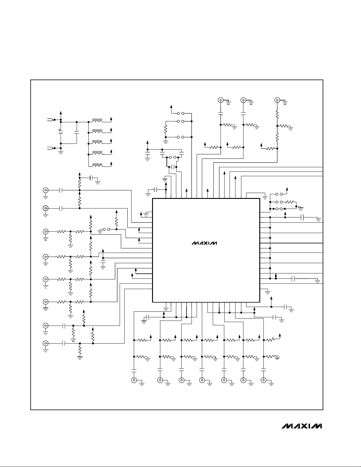
Figure1. MAX3891 EV Kit Schematic
3R3V
VCC
J46
C12
33µF
GND
J47
VCC
C1
R4
27.4Ω
R8
27.4Ω
R12
27.4Ω
R16
27.4Ω
0.1µF
C32
0.1µF
0.1µF
C2
0.1µF
C6
24.3Ω
R6
221Ω
24.3Ω
R10
221Ω
24.3Ω
R14
221Ω
24.3Ω
R18
221Ω
R32
130Ω
R5
R9
R13
R17
J1
SMA
J2
J2
SMA
SMA
J3
SMA
J4
SMA
J5
SMA
J6
SMA
J7
SMB
J8
SMB
C13
0.1µF
VCC
VCC
R1
49.9Ω
R2
49.9Ω
R40
82.5Ω
R33
130Ω
VCC
56nH
56nH
56nH
56nH
56nH
C15
0.1µF
R7
130Ω
VCC
R11
130Ω
VCC
R15
130Ω
VCC
R19
130Ω
VCC
R41
82.5Ω
L1
VCCDIG
L2
VCC0
L3
VCCPLL
L4
VCCVCO
L5
VCCPECL
GND
VCC
R3
10kΩ
JU1
VCCO
C3
0.1µF
C10
0.1µF
VCCO
VCCO
VCCDIG
C35
0.1µF
R27
82.5Ω
R26
130Ω
C16
0.1µF
VCCPLL
VCCO
VCCO
0.1µF
1
2
3
4
5
6
7
8
9
10
11
12
13
14
15
16
VCCPECL
VCC
R22
20kΩ
C9
VCCVCO
C11
0.1µF
GND
V
CC
SLBOSLBO+
V
CC
SOS
V
CC
SCLKOSCLKO+
V
CC
SDOSDO+
V
CC
V
CC
PLKI+
PLKI-
R31
82.5Ω
R30
130Ω
C17
0.1µF
VCCDIG
JU6
64
CC
V
GND
17
18
63
GND
PDI15
VCC
JU3
JU4
JU5
C7
0.33µF
62
FIL-
FIL+
VCCPDI14
19
20
0.1µF
C8
0.1µF
61
21
R35
82.5Ω
R34
130Ω
C18
VCCPLL
60
CC
V
CLKSET
CC
V
PDI13
22
VCC
VCC
58
59
RCLK-
RCLK+
U1
MAX3891
VCCPDI12
23
24
82.5Ω
130Ω
0.1µF
C19
R38
57
R39
0.1µF
R37
82.5Ω
VCCDIGV
56
CC
CC
V
J26
SMA
C5
55
PCLKO-
PDI11
26
VCC
R36
130Ω
VCC
VCCPECL
54
V
PCLKO+
VCCPDI10
272528
82.5Ω
130Ω
0.1µF
53
CC
29
R43
R42
C20
C4
0.1µF
R21
82.5Ω
VCCPECL
52
CC
V
PDI0
CC
V
30
VCC
51
J25
SMA
31
PDI1
0.1µF
R20
130Ω
50
GND
VCCVCCPDI9
32
R47
82.5Ω
R46
130Ω
C21
49
GND
PDI2
PDI3
PDI4
PDI5
PDI6
PDI7
PDI8
GND
VCC
V
CC
V
CC
V
CC
V
CC
V
CC
V
CC
V
CC
VCCPECL
VCC
J28
SMB
R29
27.4Ω
R93
221Ω
R25
24.3Ω
R95
130Ω
VCCDIG
GNDTEST
R23
JU7
20kΩ
JU8
48
JU9
VCCDIG
C34
0.1µF
VCC
VCCPECL
C36VCCPECL
C14
0.1µF
C37
0.1µF
0.1µF
47
46
45
44
43
42
41
40
39
38
37
36
35
34
33
R51
82.5Ω
R50
130Ω
C22
0.1µF
SMB
J9
J10
SMB
J11
SMB
J12
SMB
J13
SMB
J14
SMB
J15
SMB
Page 5
Evaluates: MAX3891
MAX3891 Evaluation Kit
_______________________________________________________________________________________ 5
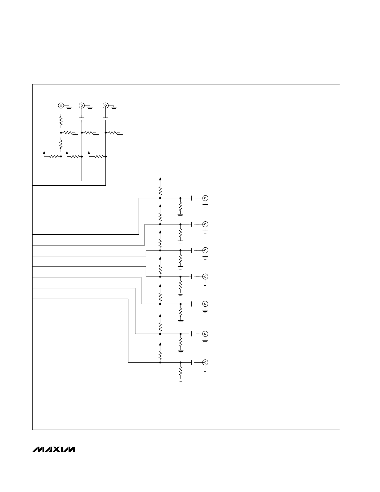
Figure1. MAX3891 EV Kit Schematic (continued)
VCC
R28
27.4Ω
R24
24.3Ω
R91
130Ω
J27
SMB
R89
221Ω
VCC
C31
0.1µF
R87
82.5Ω
J24
SMB
R85
130Ω
VCC
C30
0.1µF
R83
82.5Ω
J23
SMB
R81
130Ω
VCC
VCC
VCC
VCC
VCC
VCC
VCC
R79
82.5Ω
R75
82.5Ω
R71
82.5Ω
R67
82.5Ω
R63
82.5Ω
R59
82.5Ω
R55
82.5Ω
R78
130Ω
R74
130Ω
R70
130Ω
R66
130Ω
R62
130Ω
R58
130Ω
R54
130Ω
C29
0.1µF
C28
0.1µF
C27
0.1µF
C26
0.1µF
C25
0.1µF
C24
0.1µF
C23
0.1µF
J22
SMB
J21
SMB
J20
SMB
J19
SMB
J18
SMB
J17
SMB
J16
SMB
Page 6
Evaluates: MAX3891
MAX3891 Evaluation Kit
6 _______________________________________________________________________________________
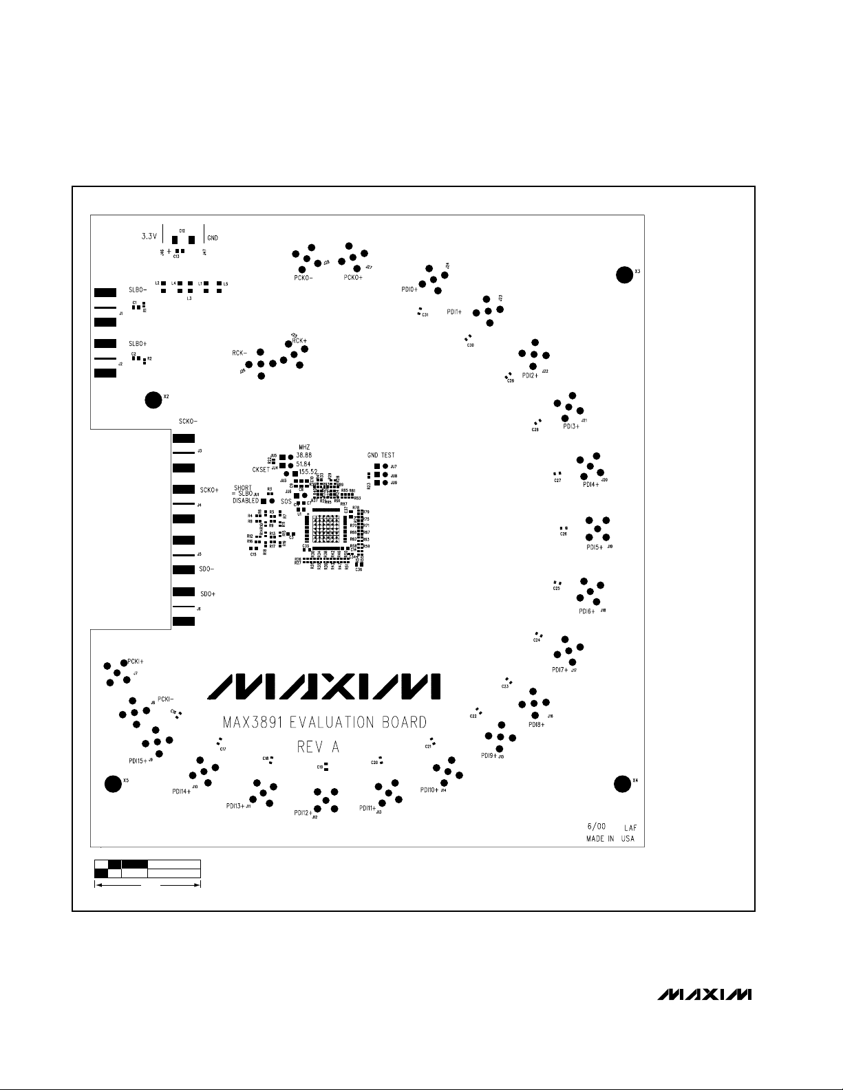
Figure 2. MAX3891 EV Kit Component Placement Guide
1.0"
Page 7
Evaluates: MAX3891
MAX3891 Evaluation Kit
_______________________________________________________________________________________ 7
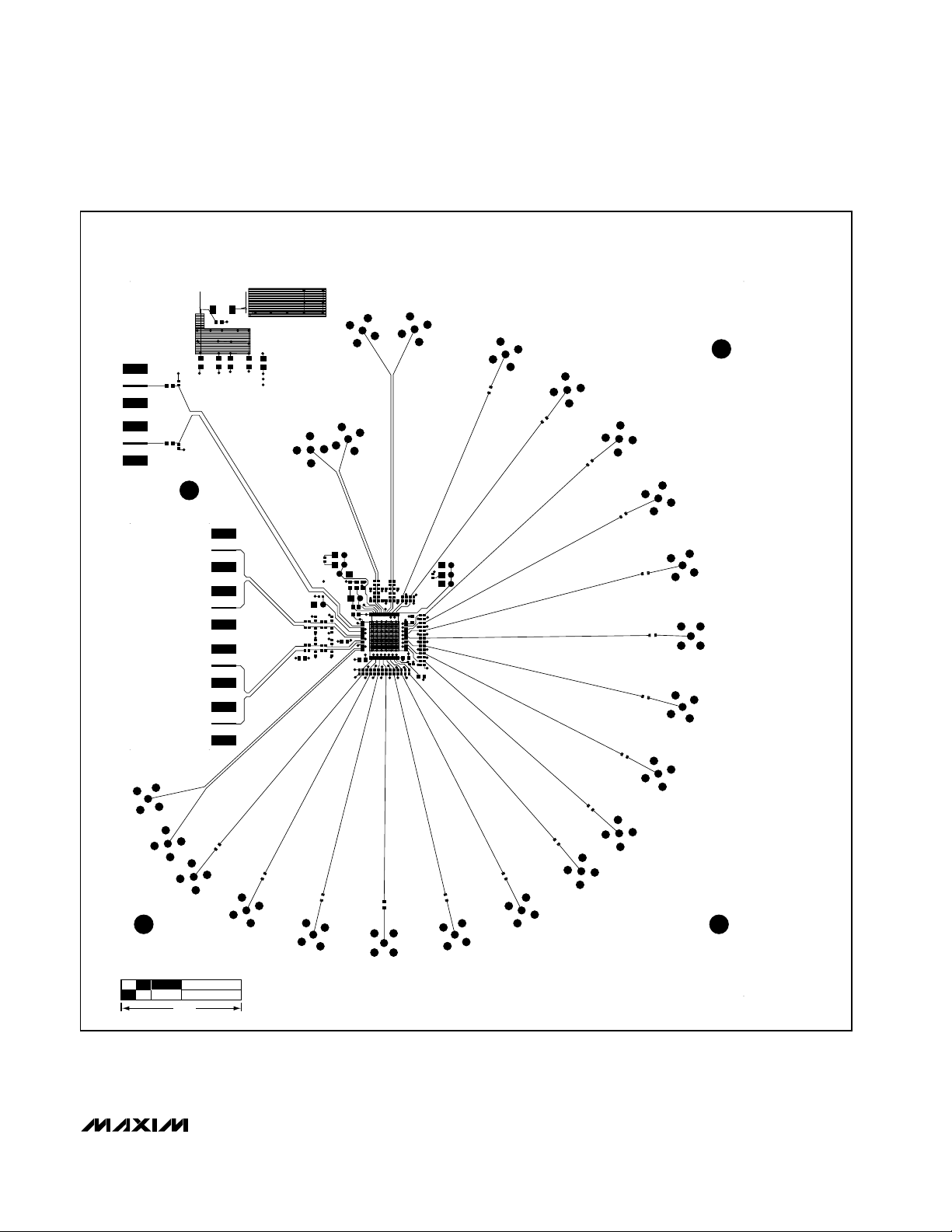
Figure 3. MAX3891 EV Kit PC Board Layout —Component Side
1.0"
Page 8

Evaluates: MAX3891
MAX3891 Evaluation Kit
8 _______________________________________________________________________________________
Figure 4. MAX3891 EV Kit PC Board Layout—Ground Plane
1.0"
Page 9

Evaluates: MAX3891
MAX3891 Evaluation Kit
Maxim cannot assume responsibility for use of any circuitry other than circuitry entirely embodied in a Maxim product. No circuit patent licenses are
implied. Maxim reserves the right to change the circuitry and specifications without notice at any time.
Maxim Integrated Products, 120 San Gabriel Drive, Sunnyvale, CA 94086 408-737-7600 _____________________ 9
© 2001 Maxim Integrated Products Printed USA is a registered trademark of Maxim Integrated Products.
Figure 5. MAX3891 EV Kit PC Board Layout—Power Plane
1.0"
 Loading...