

Page 1
For pricing, delivery, and ordering information, please contact Maxim Direct at 1-888-629-4642,
or visit Maxim’s website at www.maxim-ic.com.
General Description
The MAX3885 deserializer is ideal for converting
2.488Gbps serial data to 16-bit wide, 155Mbps parallel
data in SDH/SONET applications. Operating from a single +3.3V supply, this device accepts PECL serial
clock and data inputs, and delivers low-voltage differential-signal (LVDS) clock and data outputs for interfacing with high-speed digital circuitry. It also provides an
LVDS synchronization input that enables data realignment and reframing. The MAX3885 is available in the
extended temperature range (-40°C to +85°C) in a 64pin TQFP package.
Applications
2.488Gbps SDH/SONET Transmission Systems
Add/Drop Multiplexers
Digital Cross Connects
Features
♦♦
Single +3.3V Supply
♦♦
2.488Gbps Serial to 155Mbps Parallel Conversion
♦♦
660mW Operating Power
♦♦
LVDS Data Outputs and Synchronization Inputs
♦♦
Self-Biasing PECL Inputs Ease AC Coupling
♦♦
Synchronization Inputs for Data Realignment and
Reframing
MAX3885
+3.3V, 2.488Gbps, SDH/SONET
1:16 Deserializer with LVDS Outputs
________________________________________________________________
Maxim Integrated Products
1
19-4767; Rev 4; 12/07
Pin Configuration appears at end of data sheet.
Ordering Information
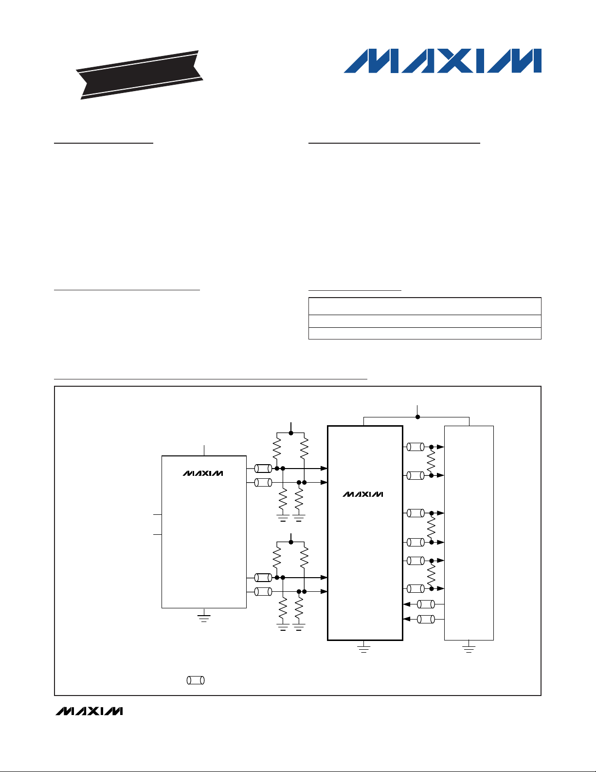
Typical Operating Circuit
+
Denotes a lead-free package.
EVALUATION KIT
AVAILABLE
VCC = +3.3V
SERIAL DATA
INPUTS
VCC = +3.3V
MAX3875
DATA
AND
CLOCK
RECOVERY
133Ω 133Ω
86.6Ω
VCC = +3.3V
133Ω 133Ω
86.6Ω
PART TEMP RANGE PIN-PACKAGE
MAX3885ECB -40°C to +85°C 64 TQFP
MAX3885ECB+ -40°C to +85°C 64 TQFP
VCC = +3.3V
V
CC
PD15+
PD15-
PD0+
PD0-
PCLK+
PCLK-
SYNC+
SYNC-
100Ω*
•
•
•
100Ω*
100Ω*
OVERHEAD
TERMINATION
86.6Ω
86.6Ω
SD+
SD-
MAX3885
SCLK+
SCLK-
GND
*REQUIRED ONLY IF OVERHEAD CIRCUIT DOES NOT INCLUDE INTERNAL INPUT TERMINATION.
THIS SYMBOL REPRESENTS A TRANSMISSION LINE OF CHARACTERISTIC IMPEDANCE Z0 = 50Ω.
Page 2
MAX3885
+3.3V, 2.488Gbps, SDH/SONET
1:16 Deserializer with LVDS Outputs
2 _______________________________________________________________________________________
ABSOLUTE MAXIMUM RATINGS
Stresses beyond those listed under “Absolute Maximum Ratings” may cause permanent damage to the device. These are stress ratings only, and functional
operation of the device at these or any other conditions beyond those indicated in the operational sections of the specifications is not implied. Exposure to
absolute maximum rating conditions for extended periods may affect device reliability.
Positive Supply Voltage (VCC)...............................-0.5V to +7.0V
Input Voltage Level (all inputs)...................-0.5V to (V
CC
+ 0.5V)
Output Current LVDS outputs .............................................10mA
Continuous Power Dissipation (T
A
= +85°C)
TQFP (derate 24mW/°C above +85°C).......................1000mW
Operating Temperature Range ...........................-40°C to +85°C
Storage Temperature Range .............................-60°C to +160°C
Lead Temperature (soldering, 10sec) .............................+300°C
DC ELECTRICAL CHARACTERISTICS
(VCC= +3.0V to +3.6V, differential loads = 100Ω ±1%, TA= -40°C to +85°C, unless otherwise noted. Typical values are at VCC= +3.3V,
T
A
= +25°C.)
Figure 1
Common-mode voltage = 50mV
Differential input voltage = 100mV
VIN= V
IH(MAX)
VIN= V
IL(MIN)
CONDITIONS
%±2.5 ±10ΔR
O
Change in Magnitude of SingleEnded Output Resistance for
Complementary Outputs
Ω40 95 140R
O
Single-Ended Output Resistance
mV±25ΔV
OS
Change in Magnitude of Output
Offset Voltage for Complementary
States
V1.125 1.275V
OS
Output Offset Voltage
mV±25Δ⎥V
OD
⎥
Change in Magnitude of Differential
Output Voltage for Complementary
States
mV250 400
⎥
V
OD⎥
Differential Output Voltage
V0.925V
OL
Output Low Voltage
V1.475V
OH
Output High Voltage
VVCC- 1.16 VCC- 0.88V
IH
Input High Voltage
mA200 280I
CC
Supply Current
Ω85 100 115R
IN
Differential Input Resistance
mV78V
HYST
Threshold Hysteresis
mV-100 100V
IDTH
Differential Input Threshold
V0 2.4V
I
Input Voltage Range
VVCC- 1.81 VCC- 1.48V
IL
Input Low Voltage
µA-900 900I
IH
Input High Current
µA-900 900I
IL
Input Low Current
UNITSMIN TYP MAXSYMBOLPARAMETER
PECL INPUTS (SD+/-, SCLK+/-)
LVDS INPUTS AND OUTPUTS (SYNC+/-, PCLK+/-, PD_+/-)
Note 1: AC Characteristics guaranteed by design and characterization.
AC ELECTRICAL CHARACTERISTICS
(V
CC
= +3.0V to +3.6V, differential loads = 100Ω ±1%, TA= -40°C to +85°C, unless otherwise noted. Typical values are at VCC= +3.3V,
T
A
= +25°C.) (Note 1, Figure 4)
CONDITIONS
ps100t
H
Serial Data Hold Time
ps100t
SU
GHz2.488f
SCLK
Maximum Serial Clock Frequency
Serial Data Setup Time
ps200 450 900t
CLK-Q
Parallel Clock-to-Data Output Delay
UNITSMIN TYP MAXSYMBOLPARAMETER
Page 3
MAX3885
+3.3V, 2.488Gbps, SDH/SONET
1:16 Deserializer with LVDS Outputs
_______________________________________________________________________________________
3
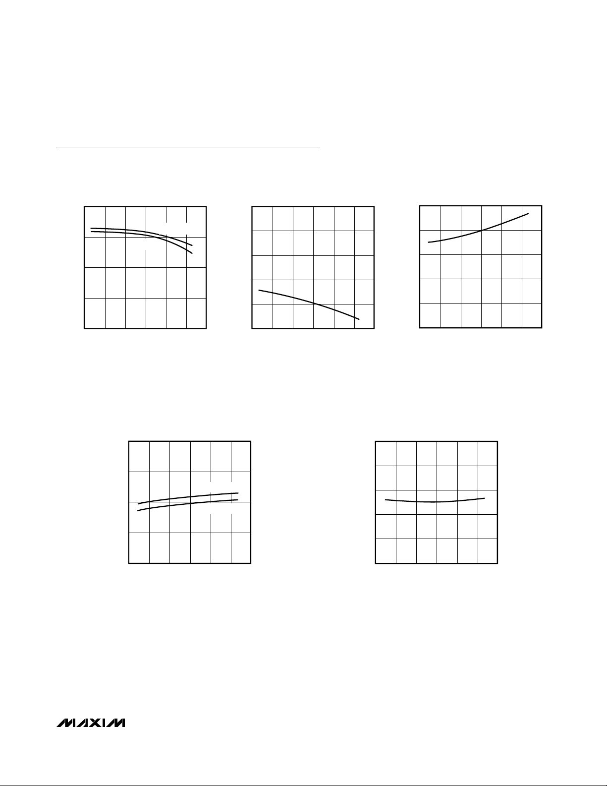
Typical Operating Characteristics
(VCC= +3.3V, TA = +25°C, unless otherwise noted.)
MAXIMUM SERIAL CLOCK FREQUENCY
vs. TEMPERATURE
4.4
4.3
4.2
4.1
MAX SERIAL CLOCK FREQUENCY (GHz)
4.0
-50 0-25 25 50 75 100
TEMPERATURE (°C)
VCC = 3.6V
VCC = 3V
100
MAX3885-01
SERIAL DATA-SETUP TIME (ps)
SUPPLY CURRENT vs. TEMPERATURE
300
SERIAL DATA-SETUP TIME
vs. TEMPERATURE
80
60
40
20
0
-50 0-25 25 50 75 100
TEMPERATURE (°C)
SERIAL DATA-HOLD TIME
vs. TEMPERATURE
0
MAX3885-02
-20
-40
-60
SERIAL DATA-HOLD TIME (ps)
-80
-100
-50 0-25 25 50 75 100
TEMPERATURE (°C)
PARALLEL CLOCK TO DATA OUTPUT
PROPAGATION DELAY vs. TEMPERATURE
700
MAX3885-03
250
VCC = 3.6V
200
SUPPLY CURRENT (mA)
150
100
-50 0-25 25 50 75 100
TEMPERATURE (°C)
VCC = 3V
MAX3885-04
600
500
400
300
PCLK TO DATA OUTPUT PROPAGATION DELAY (ps)
200
-50 0-25 25 50 75 100
TEMPERATURE (°C)
MAX3885-05
Page 4

MAX3885
+3.3V, 2.488Gbps, SDH/SONET
1:16 Deserializer with LVDS Outputs
4 _______________________________________________________________________________________
NAME FUNCTION
1, 2, 8, 16, 17,
24, 32, 33, 41,
48, 49, 57, 64
GND Ground
3, 5, 7, 9, 11,
13, 25, 34, 42,
47, 56
V
CC
+3.3V Supply Voltage
PIN
4 SD+
Serial Data Noninverting PECL Input. Data is clocked on the SCLK signal’s positive transition.
6 SD- Serial Data Inverting PECL Input. Data is clocked on the SCLK signal’s positive transition.
15 SYNC+
Synchronizing Pulse Noninverting LVDS Input. Pulse the SYNC signal high for at least four
SCLK periods to shift the data alignment by dropping one bit.
14 SYNC-
Synchronizing Pulse Inverting LVDS Input. Pulse the SYNC signal high for at least four SCLK
periods to shift the data alignment by dropping one bit.
12 SCLK- Serial Clock Inverting PECL Input
10 SCLK+ Serial Clock Noninverting PECL Input
21, 23, 27, 29,
31, 36, 38, 40,
44, 46, 51, 53,
55, 59, 61, 63
PD0+ to PD15+
Parallel Data Noninverting LVDS Outputs. Data is updated on the negative transition of the
PCLK signal.
20, 22, 26, 28,
30, 35, 37, 39,
43, 45, 50, 52,
54, 58, 60, 62
PD0- to PD15-
Parallel Data Inverting LVDS Outputs. Data is updated on the negative transition of the PCLK
signal.
19 PCLK+ Parallel Clock Noninverting LVDS Output
18 PCLK- Parallel Clock Inverting LVDS Output
Pin Description
Figure 1. Driver Output Levels
PD+
V
V
OD
+V
OD
0V
V
OD, P - P
-V
OD
V
PD-
SINGLE-ENDED OUTPUT
V
PD+
- V
V
PD+
PD-
DIFFERENTIAL OUTPUT
R
= 100Ω
D
PD-
0V (DIFF.)
L
V
|
OD|
V
OH
V
OS
V
OL
= V
- V
PD+
PD-
Page 5

MAX3885
Detailed Description
The MAX3885 deserializer uses a 16-bit shift register,
16-bit parallel output register, 4-bit counter, PECL input
buffers, and low-voltage differential-signal (LVDS)
input/output buffers to convert 2.488Gbps serial data to
16-bit wide, 155Mbps parallel data (Figure 2). The input
shift register continuously clocks incoming data on the
positive transition of the serial clock (SCLK) input signal. The 4-bit counter generates a parallel-output clock
(PCLK) by dividing the serial-clock frequency by 16.
The PCLK signal clocks the parallel-output register.
During normal operation, the counter divides the SCLK
frequency by 16, causing the output register to latch
every 16 bits of incoming serial data. The synchronization inputs (SYNC+, SYNC-) realign and reframe data.
When the SYNC signal is pulsed high for at least four
SCLK cycles, the parallel output data is delayed by one
SCLK cycle. This realignment is guaranteed to occur
within two complete PCLK cycles of the SYNC signal’s
positive transition. As a result, the first incoming bit of
data during that PCLK cycle is dropped, shifting the
alignment between PCLK and data by one bit. See
Figure 3 for the timing diagram and Figure 4 for the timing parameters diagram.
Low-Voltage Differential-Signal (LVDS)
Inputs and Outputs
The MAX3885 features LVDS inputs and outputs for
interfacing with high-speed digital circuitry. The LVDS
standard is based on the IEEE 1596.3 LVDS specification. This technology uses 500mVp-p to 800mVp-p differential low-voltage swings to achieve fast transition
times, minimize power dissipation, and improve noise
immunity. The parallel clock and data LVDS outputs
(PCLK+, PCLK-, PD_+, PD_-) require 100Ω differential
+3.3V, 2.488Gbps, SDH/SONET
1:16 Deserializer with LVDS Outputs
_______________________________________________________________________________________ 5
Figure 2. Functional Diagram
Figure 3. Timing Diagram
SD+
PECL
SD-
SCLK+
SCLK-
SYNC+
SYNC-
PECL
100Ω
LVDS
16-BIT
SHIFT
REGISTER
MAX3885
4-BIT
COUNTER
16-BIT
PARALLEL
OUTPUT
REGISTER
LVDS
LVDS
LVDS
LVDS
PD15+
PD15-
PD1+
PD1-
PD0+
PD0-
PCLK+
PCLK-
D15 D14 D13
SCLK
SYNC
PCLK
(LSB) PD0
PD1
PD15
TRANSMITTED FIRST
(MSB)
SD
D0
D1 D17 D33 D49 D66
•
•
•
D15
D16 D32 D48
ONE BIT HAS SLIPPED
IN THIS TIME SLICE
D31 D47 D64 D80
D65
Page 6

MAX3885
DC termination between the inverting and noninverting
outputs for proper operation. Do not terminate these
outputs to ground. The synchronization LVDS inputs
(SYNC+, SYNC-) are internally terminated with 100Ω
differential input resistance and, therefore, do not
require external termination.
PECL Inputs
Because of the self-biasing resistor networks, the serial
data and clock PECL inputs (SD+, SD-, SCLK+, SCLK-)
require 53Ω termination to VCC- 2V when interfacing
with a PECL source (see
Alternative PECL Input
Termination
). This results in an equivalent input resis-
tance of 50Ω.
Applications Information
Alternative PECL Input Termination
Figure 5 shows alternative PECL input-termination
methods. Use Thevenin-equivalent termination when a
VCC- 2V termination voltage is not available. When
interfacing with an ECL-output device, the MAX3885’s
internal self-biasing allows easy ECL AC-coupling termination.
Layout Techniques
For best performance, use good high-frequency layout
techniques. Filter voltage supplies and keep ground
connections short. Use multiple vias where possible.
Also, use controlled impedance transmission lines to
interface with the MAX3885 high-speed inputs and outputs.
+3.3V, 2.488Gbps, SDH/SONET
1:16 Deserializer with LVDS Outputs
6 _______________________________________________________________________________________
Figure 5. Alternative PECL Input Termination
Figure 4. Timing Parameters
t
= 1 / f
SCLK
SCLK
SCLK
SD
PCLK
PD0–PD15
NOTE: SIGNALS SHOWN ARE DIFFERENTIAL. FOR EXAMPLE, SCLK = (SCLK+) - (SCLK-).
t
CLK-Q
t
SU
THEVENIN-EQUIVALENT TERMINATION
+3.3V
133Ω
= 50Ω
Z
O
ZO = 50Ω
86.6Ω
t
H
133Ω
MAX3885
PECL
INPUTS
86.6Ω
ECL AC-COUPLING TERMINATION
ZO = 50Ω
Z
= 50Ω
O
53Ω
-2V
53Ω
-2V
MAX3885
PECL
INPUTS
Page 7

MAX3885
+3.3V, 2.488Gbps, SDH/SONET
1:16 Deserializer with LVDS Outputs
_______________________________________________________________________________________ 7
___________________Chip Information
TRANSISTOR COUNT: 2820
4243444546 3839404147
22
23
24
25
26
27
28
29
30
31
3637
33
3435
17
18
19
20
21
32
48
7654311109821312 1615141
59
58
57
56
55
54
53
52
51
50
64
63
62
61
60
49
MAX3885
PD13+
PD13-
GND
V
CC
PD12+
PD12-
GND
PD15+
PD15-
PD14+
PD14-
PD11+
PD11-
PD10+
PD10-
GND
V
CC
SCLK+
V
CC
GND
V
CC
SD-
GND
SYNC+
SYNC-
V
CC
SCLK-
V
CC
SD+
V
CC
GND
GND
PD4+
PD4-
PD3+
PD3-
PD2+
PD2-
V
CC
GND
PD1+
PD1-
PD0+
PD0-
PCLK+
PCLK-
GND
GND
V
CC
TOP VIEW
PD9+
PD9-
PD8+
PD8-
VCCGND
PD7+
PD7-
PD6+
PD6-
PD5+
PD5-
VCCGND
GND
TQFP
Pin Configuration
Package Information
(For the latest package outline information, go to
www.maxim-ic.com/packages
.)
PACKAGE TYPE DOCUMENT NO.
64 TQFP
21-0054
Page 8

MAX3885
+3.3V, 2.488Gbps, SDH/SONET
1:16 Deserializer with LVDS Outputs
Maxim cannot assume responsibility for use of any circuitry other than circuitry entirely embodied in a Maxim product. No circuit patent licenses are
implied. Maxim reserves the right to change the circuitry and specifications without notice at any time.
8
_____________________Maxim Integrated Products, 120 San Gabriel Drive, Sunnyvale, CA 94086 408-737-7600
© 2007 Maxim Integrated Products is a registered trademark of Maxim Integrated Products.
Revision History
REVISIO N
NUMBER
0 9/98 Initial release. —
REVISIO N
DATE
DESCRIPTION
PAGES
CHANGED
1 9/98
2 1/99 Corrected Figure 3. 5
3 2/07 Added lead-free package to Ordering Information table. 1
4 12/07 Replaced package drawing with table. 8
Updated Typical Operating Circuit 1
Updated Figure 3. 5
 Loading...