

Page 1
MAX3882A
2.488Gbps 1:4 Demultiplexer with Clock and
Data Recovery and Limiting Amplifier
________________________________________________________________
Maxim Integrated Products
1
For pricing, delivery, and ordering information, please contact Maxim Direct at 1-888-629-4642,
or visit Maxim’s website at www.maxim-ic.com.
General Description
The MAX3882A is a deserializer combined with clock
and data recovery and limiting amplifier ideal for converting 2.488Gbps serial data to 4-bit-wide, 622Mbps
parallel data for SDH/SONET applications. The device
accepts serial NRZ input data as low as 10mV
P-P
of
2.488Gbps and generates four parallel LVDS data outputs at 622Mbps. Included is an additional high-speed
serial data input for system loopback diagnostic testing. For data acquisition, the MAX3882A does not
require an external reference clock. However, if needed, the loopback input can be connected to an external
reference clock of 155MHz or 622MHz to maintain a
valid clock output in the absence of input data transitions. Additionally, a TTL-compatible loss-of-lock output
is provided. The device provides a vertical threshold
adjustment to compensate for optical noise generated
by EDFAs in WDM transmission systems. The
MAX3882A operates from a single +3.3V supply and
consumes 610mW.
The MAX3882A’s jitter performance exceeds all SDH/
SONET specifications. The device is available in a 6mm
✕ 6mm, 36-pin TQFN package.
Applications
SDH/SONET Receivers and Regenerators
Add/Drop Multiplexers
Digital Cross-Connects
SDH/SONET Test Equipment
DWDM Transmission Systems
Features
♦ No Reference Clock Required for Data Acquisition
♦ Serial Input Rate: 2.488Gbps
♦ Fully Integrated Clock and Data Recovery with
Limiting Amplifier and 1:4 Demultiplexer
♦ Parallel Output Rate: 622Mbps
♦ Differential Input Range: 10mV
P-P
to 1.6V
P-P
without Threshold Adjust
♦ Differential Input Range: 50mV
P-P
to 600mV
P-P
with Threshold Adjust
♦ 0.65UI High-Frequency Jitter Tolerance
♦ Loss-of-Lock (LOL) Indicator
♦ Wide Input Threshold Adjust Range: ±170mV
♦ Maintain Valid Clock Output in Absence of Data
Transitions
♦ System Loopback Input Available for System
Diagnostic Testing
♦ Operating Temperature Range -40°C to +85°C
♦ Low Power Dissipation: 610mW at +3.3V
19-2718; Rev 2; 4/09
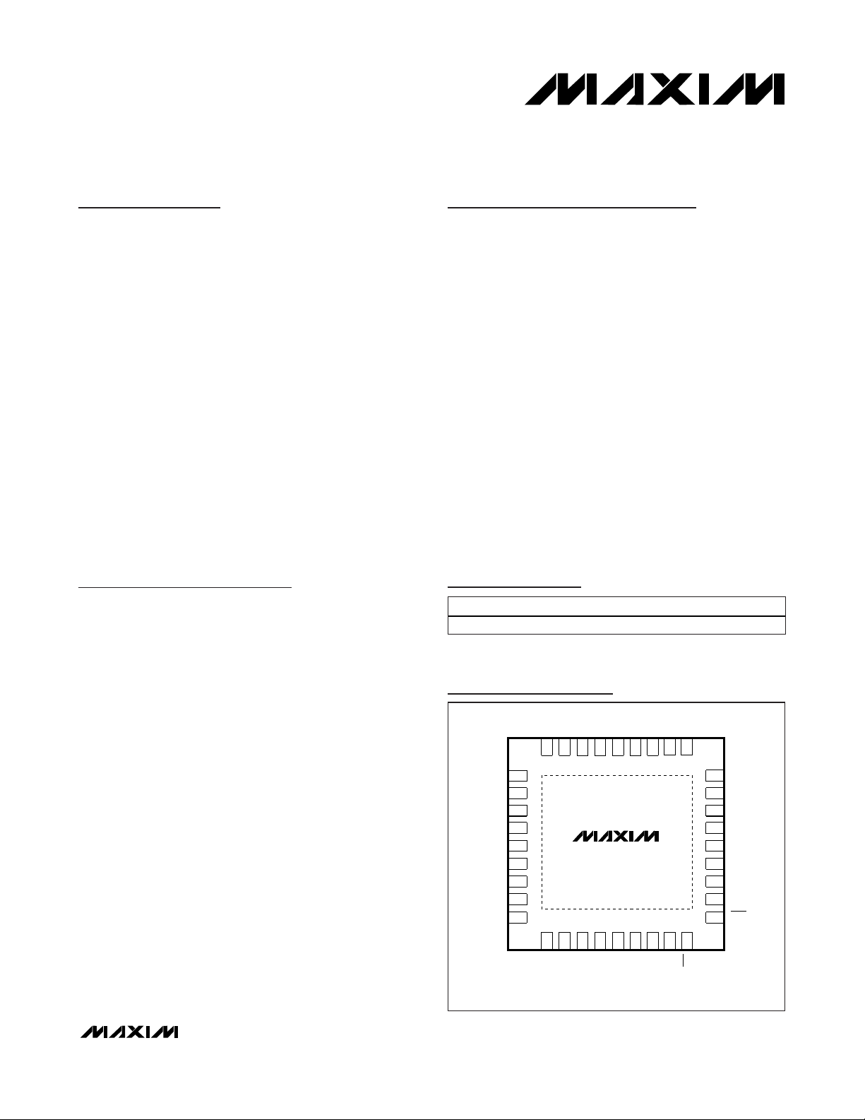
Pin Configuration
+
Denotes a lead(Pb)-free/RoHS-compliant package.
*
EP = Exposed pad.
Ordering Information
Typical Application Circuits appear at end of data sheet.
PART TEMP RANGE PIN-PACKAGE
MAX3882AETX+ -40°C to +85°C 36 TQFN-EP*
TOP VIEW
GND
PD2-
PD2+
PD3-
PD3+
27 26 25 24 23 22 21 20 19
PD1+
PD1-
PD0+
PD0-
18 PCLK+
17
PCLK-
16
GND
15
_OUT
V
CC
14
V
_VCO
CC
13
FIL
V
12
_VCO
CC
GND
11
*EP
10 LREF
SIS
LOL
VCC_OUT
GND
FREFSET
V
CC
V
CC
CAZ+
CAZ-
V
REF
V
CTRL
*EXPOSED PAD.
28
29
30
31
32
33
34
35
36
+
123456789
GND
CC
V
MAX3882A
SDI-
SDI+
TQFN
CC
V
SLBI+
SLBI-
Page 2
MAX3882A
2.488Gbps 1:4 Demultiplexer with Clock and
Data Recovery and Limiting Amplifier
2 _______________________________________________________________________________________
ABSOLUTE MAXIMUM RATINGS
Stresses beyond those listed under “Absolute Maximum Ratings” may cause permanent damage to the device. These are stress ratings only, and functional
operation of the device at these or any other conditions beyond those indicated in the operational sections of the specifications is not implied. Exposure to
absolute maximum rating conditions for extended periods may affect device reliability.
Supply Voltage, VCC................................................-0.5 to +5.0V
Input Voltage Levels
(SDI+, SDI-, SLBI+, SLBI-) ...........(V
CC
- 1.0V) to (V
CC
+ 0.5V)
Input Current Levels (SDI+, SDI-, SLBI+, SLBI-)..............±20mA
LVDS Output Voltage Levels
(PCLK±, PD_±).......................................-0.5V to (V
CC
+ 0.5V)
Voltage at LOL, SIS, LREF, V
REF
, FIL, CAZ+,
CAZ-, V
CTRL
, FREFSET ..........................-0.5V to (V
CC
+ 0.5V)
Continuous Power Dissipation (T
A
= +70°C)
36-Pin TQFN (derate 35.7mW/°C above +70°C) ......2856mW
Operating Temperature Range ...........................-40°C to +85°C
Storage Temperature Range .............................-55°C to +150°C
Lead Temperature (soldering, 10s) .................................+300°C
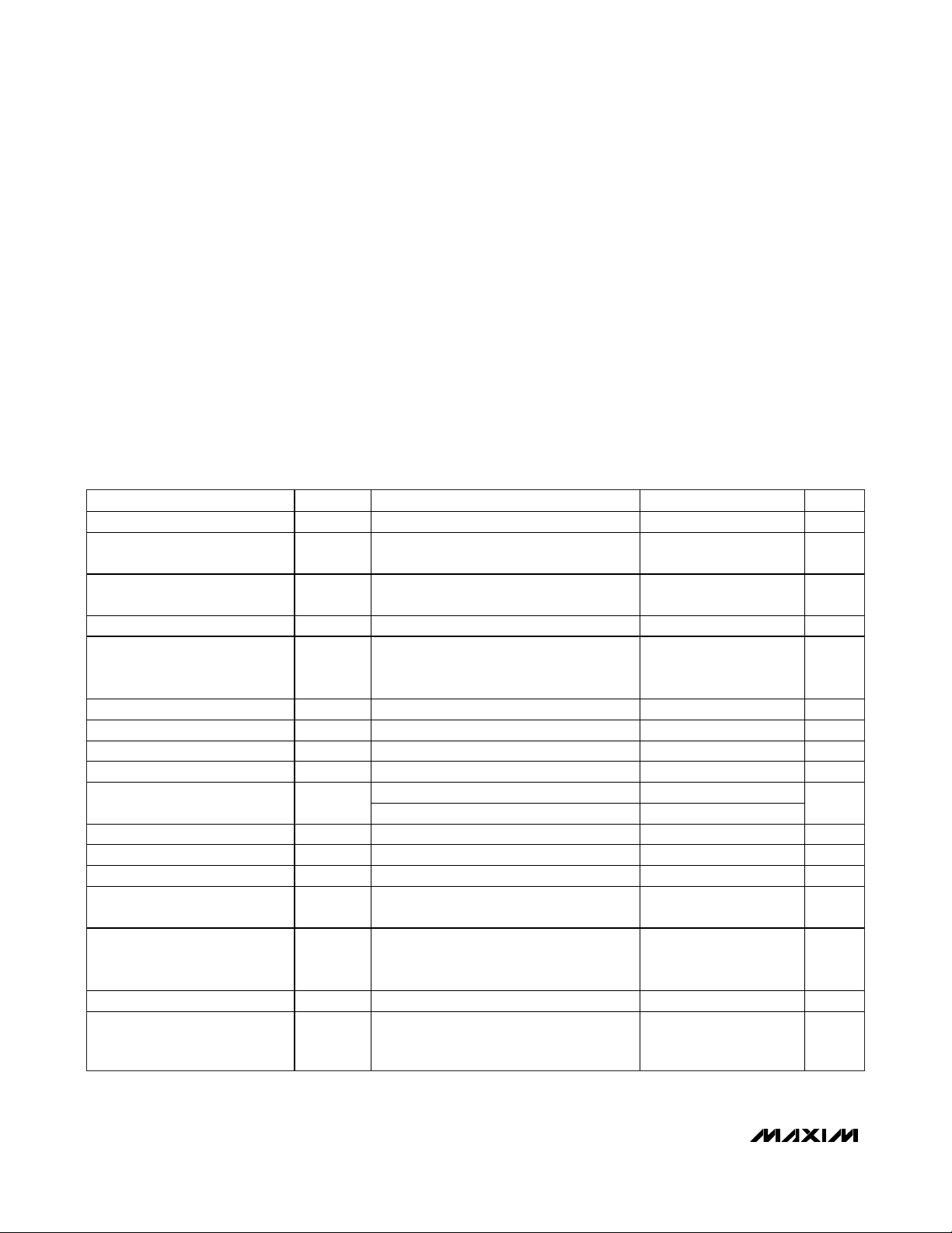
DC ELECTRICAL CHARACTERISTICS
(VCC= +3.0 to +3.6V, TA= -40°C to +85°C. Typical values are at +3.3V and at TA= +25°C, unless otherwise noted.) (Note 1)
Supply Current ICC 185 230 mA
Single-Ended Input Voltage
Range
Input Common-Mode Voltage
Range
Input Termination to VCC R
Differential Input Voltage Range
with Threshold Adjust Enabled
SDI+, SDI-
Threshold Adju stment Range VTH Figure 2 -170 +170 mV
Threshold-Control Voltage V
Threshold-Control Linearity ±5 %
Threshold Setting Accuracy Figure 2 -18 +18 mV
Threshold Setting Stability
V
REF
LVDS Output High Voltage VOH 1.475 V
LVDS Output Low Voltage V
PARAMETER SYMBOL CONDITIONS MIN TYP MAX UNITS
V
CTRL
Voltage Output RL = 50k 2.14 2.2 2.24 V
OL
Figure 1
IS
Figure 1
42.5 50 57.5
IN
Figure 2 100 600 mV
(Note 2) 0.302 2.097 V
15mV |VTH| 80mV -6 +6
80mV < |V
0.925 V
TH
| 170mV -12 +12
V
0.8
V
0.4
CC
CC
-
-
V
CC
0.4
V
CC
+
V
V
P-P
mV
LVDS Differentia l Output Voltage |VOD| 250 400 mV
LVDS Change in Magnitude of
Differential Output Voltage for
Complementary States
LVDS Offset Output Voltage 1.125 1.275 V
LVDS Change in Magnitude of
Output Offset Voltage for
Complementary States
|V
| 25 mV
OD
|V
| 25 mV
OS
Page 3
MAX3882A
2.488Gbps 1:4 Demultiplexer with Clock and
Data Recovery and Limiting Amplifier
_______________________________________________________________________________________ 3
DC ELECTRICAL CHARACTERISTICS (continued)
(VCC= +3.0 to +3.6V, TA= -40°C to +85°C. Typical values are at +3.3V and at TA= +25°C, unless otherwise noted.) (Note 1)
Note 1: At -40°C, DC characteristics are guaranteed by design and characterization.
Note 2: Voltage applied to V
CTRL
pin is from 0.302V to 2.097V when input threshold is adjusted from +170mV to -170mV.
AC ELECTRICAL CHARACTERISTICS
(VCC= +3.0 to +3.6V, TA= -40°C to +85°C. Typical values are at +3.3V and at TA= +25°C, unless otherwise noted.) (Note 3)
LVDS Differentia l Output
Impedance
LVDS Output Current Short together or short to GND 12 mA
LVTTL Input High Voltage VIH 2.0 V
LVTTL Input Low Voltage VIL 0.8 V
LVTTL Input Current -10 +10 μA
LVTTL Output High Voltage VOH IOH = +20μA 2.4 V
LVTTL Output Low Voltage VOL IOL = -1mA 0.4 V
PARAMETER SYMBOL CONDITIONS MIN TYP MAX UNITS
80 120
Serial Input Data Rate 2.488 Gbps
Differential Input Voltage
Threshold Adjust Disabled
SDI+, SDI-
PARAMETER SYMBOL CONDITIONS MIN TYP MAX UNITS
V
(Note 4) Figure 1 10 1600 mV
ID
P-P
Differential Input Voltage SLBI+,
SLBI-
Jitter Peaking JP f 2MHz 0.1 dB
Jitter Transfer Bandwidth JBW 1.7 2.0 MHz
Sinusoidal Jitter Tolerance
Sinusoidal Jitter To lerance with
Threshold Adjust Enabled
(Note 5)
Jitter Generation J
Differential Input Return Loss 20 log|S11|
Tolerated Consecutive Identical
Digits
Acquisition Time (Note 7)
Figure 4
LOL As sert Time Figure 4 2.3 100.0 μs
Low-Frequency Cutoff for
DC Offset Cancellation Loop
50 800 mV
f = 100kHz 3.1 4.1
f = 1MHz 0.62 1.0
f = 10MH z 0.44 0.6
f = 100kHz 4.1
f = 1MHz 0.75
f = 10MH z 0.41
(Note 6) 2.7 ps
GEN
100kHz to 2.5GHz 17
2.5GHz to 4.0GHz 15
BER = 10
0011 pattern 0.6
PRBS 2
CAZ = 0.1μF 4 kHz
-10
2000 Bits
23
- 1 pattern 0.62 1.5
UI
UI
P-P
P-P
P-P
RMS
dB
ms
Page 4
MAX3882A
2.488Gbps 1:4 Demultiplexer with Clock and
Data Recovery and Limiting Amplifier
4 _______________________________________________________________________________________
AC ELECTRICAL CHARACTERISTICS (continued)
(VCC= +3.0 to +3.6V, TA= -40°C to +85°C. Typical values are at +3.3V and at TA= +25°C, unless otherwise noted.) (Note 3)
Note 3: AC characteristics are guaranteed by design and characterization.
Note 4: Jitter tolerance is guaranteed (BER ≤ 10
-10
) within this input voltage range. Input threshold adjust is disabled when V
CTRL
is
connected to V
CC
.
Note 5: Measured with the input amplitude set at 100mV
P-P
differential swing with a 20mV offset and an input edge speed of 145ps
(4th-order Bessel filter with f
3dB
= 1.8GHz).
Note 6: Measured with 10mV
P-P
OC-48 differential input with PRBS 223- 1 and BW = 12kHz to 20MHz.
Note 7: Measured at OC-48 data rate using a 0.068µF loop-filter capacitor.
Note 8: Under LOL condition, the CDR clock output is set by the external reference clock.
Note 9: Relative to the falling edge of PCLK+. See Figure 3.
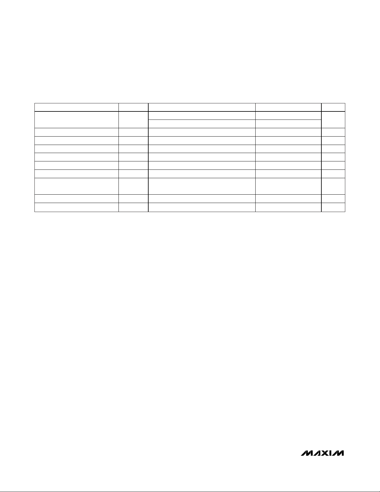
Reference Cloc k Frequenc y
Reference Clock Accuracy ±100 ppm
VCO Frequency Drift (Note 8) 400 ppm
Data Output Rate 622 Mbps
Cloc k Output Frequenc y 622 MHz
Output Cloc k-to-Data Dela y t
Cloc k Output Duty Cycle 45 50 55 %
Clock and Data Output Rise/Fall
Time
LVDS Differentia l Skew t
LVDS Channel-to-Channel Skew t
PARAMETER SYMBOL CONDITIONS MIN TYP MAX UNITS
FREFSET = VCC 155
FREFSET = GND 622
(Note 9) -80 +80 ps
CK-Q
, t
t
R
SKEW1
SKEW2
20% to 80% 100 250 ps
F
Any differential pair 50 ps
PD_± 100 ps
MHz
Page 5

MAX3882A
2.488Gbps 1:4 Demultiplexer with Clock and
Data Recovery and Limiting Amplifier
_______________________________________________________________________________________
5
Typical Operating Characteristics
(TA = +25°C, unless otherwise noted.)
500ps/div
RECOVERED CLOCK AND DATA
(INPUT = 2.488Gbps, 2
23
- 1
PATTERN, V
IN
= 10mV
P-P
)
200mV/div
MAX3882A toc01
SUPPLY CURRENT vs. TEMPERATURE
MAX3882A toc02
TEMPERATURE (°C)
SUPPLY CURRENT (mA)
7550250-25
170
180
190
200
210
220
230
240
250
260
160
-50 100
JITTER TOLERANCE
(2.48832Gbps, 2
23
- 1 PATTERN,
V
IN
= 16mV
P-P
WITH ADDITIONAL
0.15UI DETERMINISTIC JITTER)
MAX3882A toc03
JITTER FREQUENCY (Hz)
JITTER TOLERANCE (UI
P-P
)
100 1k
1
10
100
0.1
10 10k
BELLCORE
MASK
JITTER TOLERANCE vs. INPUT AMPLITUDE
(2.48832Gbps, 2
23
- 1 PATTERN, WITH
ADDITIONAL 0.15UI DETERMINISTIC JITTER)
MAX3882A toc04
INPUT AMPLITUDE (mV
P-P
)
JITTER TOLERANCE (UI
P-P
)
100010010
0.1
0.2
0.3
0.4
0.5
0.6
0
1 10,000
JITTER FREQUENCY = 10MHz
JITTER TRANSFER
MAX3882A toc05
JITTER FREQUENCY (kHz)
TRANSFER (dB)
100010010
-35
-30
-25
-20
-15
-10
-5
0
5
-40
1 10,000
BELLCORE
MASK
20ps/div
PARALLEL CLOCK OUTPUT JITTER
MAX3882A toc06
f
CLK
= 622.08MHz
TOTAL WIDEBAND
RMS JITTER = 2.720ps
PEAK-TO-PEAK
JITTER = 20.80ps
BIT-ERROR RATE vs. INPUT AMPLITUDE
MAX3882A toc07
INPUT VOLTAGE (mV
P-P
)
BIT-ERROR RATIO
432
1.00E-10
1.00E-09
1.00E-08
1.00E-07
1.00E-06
1.00E-05
1.00E-04
1.00E-11
15
PULLIN RANGE
MAX3882A toc08
AMBIENT TEMPERATURE (°C)
FREQUENCY (GHz)
603510-15
2.1
2.2
2.3
2.4
2.5
2.6
2.7
2.8
2.9
3.0
2.0
-40 85
S11
MAX3882A toc09
FREQUENCY (MHz)
dB
350030002500200015001000500
-30
-20
-10
0
10
20
-40
0 4000
Page 6

MAX3882A
2.488Gbps 1:4 Demultiplexer with Clock and
Data Recovery and Limiting Amplifier
6 _______________________________________________________________________________________
Pin Description
PIN NAM E FUNCTION
1, 11, 16, 23, 29 GND Supply Ground
2, 5, 31, 32 VCC +3.3V Supply Voltage
3 SDI+ Positive Data Input. 2.488Gbps serial data stream, CML.
4 SDI- Negative Data Input. 2.488Gbps serial data stream, CML.
6 SLBI+ Posit ive System Loopback Input or Positive Reference C lock Input, CML
7 SLBI- Negative System Loopback Input or Negative Reference Clock Input, CML
8 SIS Signal Input Selection, LVTTL. Low for normal data, high for sy stem loopback.
9 LOL Loss-of-Lock Output, LVTTL, Active Low
10 LREF
12, 14 VCC_VCO Supply Voltage for the VCO
13 FIL
15, 28 VCC_OUT Supply Voltage for LVDS Output Buffer s
17 PCLK- Negative Cloc k Output, LVDS
18 PCLK+ Positive C lock Output, LVDS
19 PD0- Negative Data Output, LVDS
20 PD0+ Positive Data Output, LVDS
21 PD1- Negative Data Output, LVDS
22 PD1+ Positive Data Output, LVDS
24 PD2- Negative Data Output, LVDS
25 PD2+ Positive Data Output, LVDS
26 PD3- Negative Data Output, LVDS, MSB
27 PD3+ Positive Data Output, LVDS, MSB
30 FREFSET
33 CAZ+
34 CAZ-
35 V
36 V
— EP
2.2V Bandgap Reference Voltage Output. Optional ly used for threshold ad justment.
REF
CTRL
TTL Control Input for PLL Clock Holdover. Low for PLL lock to reference cloc k, high for PLL
loc k to input data.
PLL Loop-Fi lter Capacitor Input. Connect a 0.068μF loop-filter capac itor between FIL and
V
VCO.
CC_
Sets Reference Frequency. LVTTL low for 622MHz/667MHz reference, h igh for
155MHz/167MHz reference.
Positive Capacitor Input for DC Offset-Cancellation Loop. Connect a 0.1μF capacitor
between CAZ+ and CAZ-.
Negative Capacitor Input for DC Offset-Cance llation Loop. Connect a 0.1μF capac itor
between CAZ+ and CAZ-.
Analog Control Input for Threshold Adju stment. Connect to VCC to disable threshold adjust.
Exposed Pad. The exposed pad must be soldered to the circuit board ground for proper
thermal and electrical performance.
Page 7

Detailed Description
The MAX3882A deserializer with clock and data recovery and limiting amplifier converts 2.488Gbps serial
data to clean 4-bit-wide, 622Mbps LVDS parallel data.
The device combines a limiting amplifier with a fully integrated phase-locked loop (PLL), data retiming block, 4bit demultiplexer, clock divider, and LVDS output buffer
(Figure 5). The PLL consists of a phase/frequency
detector (PFD), loop filter, and voltage- controlled oscillator (VCO). The MAX3882A is designed to deliver the
best combination of jitter performance and power dissi-
pation by using a fully differential signal architecture
and low-noise design techniques.
The input signal to the device (SDI) passes through a
DC offset control block, which balances the input signal
to a zero crossing at 50%. The PLL recovers the serial
clock from the serial input data stream and produces
the properly aligned data and the buffered recovered
clock. The frequency of the recovered clock is divided
by four and converted to differential LVDS parallel output PCLK. The demultiplexer generates 4-bit-wide
622Mbps parallel data.
MAX3882A
2.488Gbps 1:4 Demultiplexer with Clock and
Data Recovery and Limiting Amplifier
_______________________________________________________________________________________ 7
Figure 1. Definition of Input Voltage Swing
Figure 2. Relationship Between Control Voltage and Threshold
Voltage
Figure 3. Definition of Clock-to-Q Delay
Figure 4. LOL Assert Time and PLL Acquisition Time
Measurement
V
+ 0.4V
CC
5mV
5mV
V
VCC - 0.4V
V
VCC - 0.4V
V
- 0.8V
CC
800mV
CC
(a) AC-COUPLED SINGLE-ENDED INPUT
CC
800mV
(b) DC-COUPLED SINGLE-ENDED INPUT
(mV)
V
TH
+188
+170
+152
-152
-170
-188
0.3
1.1
THRESHOLD-SETTING ACCURACY
(PART-TO-PART VARIATION OVER PROCESS)
1.3
2.1
THRESHOLD-SETTING STABILITY
(OVER TEMPERATURE AND POWER SUPPLY)
V
CTRL
(V)
t
CK
PCLK+
t
CK-Q
(PD+) - (PD-)
2.488Gbps PRBS 2
INPUT DATA
LOL ASSERT TIME
LOL OUTPUT
23
- 1 2.488Gbps PRBS 223 - 1
ACQUISITION TIME
Page 8

MAX3882A
Input Amplifier
The SDI inputs of the MAX3882A accept serial NRZ
data at 2.488Gbps with 10mV
P-P
to 1600mV
P-P
ampli-
tude. The input sensitivity is 10mV
P-P
, at which the jitter
tolerance is met for a BER of 10
-10
when the threshold
adjust is not used. The input sensitivity is as low as
4mV
P-P
for a BER of 10
-10
. The MAX3882A is designed
to directly interface with a transimpedance amplifier
(MAX3277).
For applications when vertical threshold adjustment is
needed, the MAX3882A can be connected to the output of an AGC amplifier (MAX3861). Here, the input
voltage range is 50mV
P-P
to 600mV
P-P
. See the
Design
Procedure
section for decision threshold adjust.
Phase Detector
The phase detector in the MAX3882A produces a voltage proportional to the phase difference between the
incoming data and the internal clock. Because of its
feedback nature, the PLL drives the error voltage to
zero, aligning the recovered clock to the center of the
incoming data eye for retiming.
Frequency Detector
The digital frequency detector (FD) acquires frequency
lock without using an external reference clock. The frequency difference between the received data and the
VCO clock is derived by sampling the in-phase and
quadrature VCO outputs on both edges of the data
input signal. Depending on the polarity of the frequency
difference, the FD drives the VCO until the frequency
difference is reduced to zero. Once frequency acquisition is complete, the FD returns to a neutral state. False
locking is eliminated by this digital frequency detector.
Loop Filter and VCO
The fully integrated PLL has a second-order transfer
function, with a loop bandwidth (fL) fixed at 1.7MHz. An
external capacitor between V
CC_
VCO and FIL sets the
damping of the PLL. All jitter specifications are based
on the C
FIL
capacitor being 0.068µF. Note that the PLL
jitter transfer bandwidth does not change as the external capacitor changes, but the jitter peaking, acquisition time, and loop stability are affected.
For an overdamped system (f
Z/fL
) < 0.25, the jitter
peaking (J
P
) of a second-order system can be approxi-
mated by:
J
P
= 20log(1 + fZ/fL)
The PLL zero frequency (f
Z
) is a function of the external
capacitor (CFIL) and can be approximated according to:
fZ= 1/2π(650)C
FIL
Figures 6 and 7 show the open-loop and closed-loop
transfer functions. The PLL acquisition time is also
directly proportional to the external capacitor C
FIL
.
Loss-of-Lock Monitor
The LOL output indicates a PLL lock failure, either due
to excessive jitter present at data input or due to loss of
input data. In the case of loss of input data, the LOL
indicates a loss-of-signal condition. The LOL output is
asserted low when the PLL loses lock.
Output LVDS Interface: PD, PCLK
The MAX3882A’s clock and data outputs are LVDS
compatible to minimize power dissipation, speed transition time, and improve noise immunity. These outputs
comply with the IEEE LVDS specification. The differential output signal magnitude is 250mV to 400mV.
Design Procedure
The MAX3882A provides a differential output clock
(PCLK). Table 1 shows the pin configuration for choosing the type of operation mode.
Decision Threshold Adjust
Decision threshold adjust is available for WDM applications where optical amplifiers are used, generating
spontaneous optical noise at data logic high. The decision threshold adjust range is ±170mV. Use the provided 2.2V bandgap reference V
REF
pin or an outside
source, such as an output from a DAC to control the
2.488Gbps 1:4 Demultiplexer with Clock and
Data Recovery and Limiting Amplifier
8 _______________________________________________________________________________________
Table 1. Operation Modes
FREF SET LREF SIS OPERATION MODE DESCRIPTION
X 1 0 Normal operation: PLL locked to data input at 2.488Gbps
X 1 1 System loopback: PLL lock frequency at 2.488Gbps
1 0 X Cloc k holdover: PLL loc ked to reference frequenc y at 155MHz
0 0 X Cloc k holdover: PLL loc ked to reference frequenc y at 622MHz
Page 9

threshold voltage. The +170mV to -170mV threshold
offset can be accomplished by varying the V
CTRL
voltage from 0.3V to 2.1V, respectively. See Figure 2.
When using the V
REF
to generate voltage for threshold
setting, see Figure 8. Connect V
CTRL
directly to VCCto
disable threshold adjust.
DC-Offset Cancellation Loop Filter
A DC-offset cancellation loop is implemented to remove
the DC offset of the limiting amplifier. To minimize the
low-frequency pattern-dependent jitter associated with
this DC-cancellation loop, the low-frequency cutoff is
10kHz typical with CAZ = 0.1µF, connected across
CAZ+ and CAZ-.
MAX3882A
2.488Gbps 1:4 Demultiplexer with Clock and
Data Recovery and Limiting Amplifier
_______________________________________________________________________________________ 9
Figure 5. Functional Diagram
Figure 6. Open-Loop Transfer Function
Figure 7. Closed-Loop Transfer Function
V
REF
SDI+
SDI-
V
CTRL
SLBI+
SLBI-
LREF
SIS
FREFSET
BANDGAP
REFERENCE
AMP
LOGIC
AMP
CAZ
CAZ+ CAZ-
DC OFFSET
CANCELLATION
PFD
FIL
LOL
LPF
V
PDO+
LVDS
MAX3882A
0
DCKQ
1
VCO
PLL
CC
4-BIT
DEMULTIPLEXER
DIV/4
LVDS
LVDS
LVDS
LVDS
PDO-
PD1+
PD1-
PD2+
PD2-
PD3+
PD3-
PCLK+
PCLK-
HO(j2πf) (dB)
C
= 0.01μF
C
= 0.068μF
FIL
OPEN-LOOP GAIN
= 3.6kHz
f
Z
1
FIL
= 2.45kHz
f
Z
10 100 1000
f = (kHz)
= 0.01μF
C
(j2πf) (dB)
H
O
0
-3
CLOSED-LOOP GAIN
1
C
FIL
10 100 1000
FIL
= 0.068μF
f = (kHz)
Page 10

MAX3882A
Applications Information
Clock Holdover Capability
Clock holdover is required in some applications where
a valid clock needs to be provided to the upstream
device in the absence of data transitions. To provide
this function, an external reference clock rate of
155MHz or 622MHz must be applied to the SLBI input.
Control input FREFSET selects which reference clock
rate to use. The control LREF selects whether the PLL
locks to the input data stream (SDI) or the reference
clock (SLBI). When LREF is low, the input is switched
to the reference clock input. This LREF input can be
driven by connecting the LOL output pin directly or
connecting to any other power monitor signal from the
system.
System Loopback
The MAX3882A is designed to allow system loopback
testing. The user can connect the serializer output
(MAX3892) directly to the SLBI± inputs of the
MAX3882A for system diagnostics. See Table 1 for
selecting the system loopback operation mode. During
system loopback, LOL cannot be connected to LREF.
Interfacing the MAX3882A
To correctly interface with the MAX3882A’s CML input
and LVDS outputs, refer to Application Note 291:
HFAN-1.0: Introduction to LVDS, PECL, and CML
.
Layout Techniques
For best performance, use good high-frequency layout
techniques. Filter voltage supplies, keep ground connections short, and use multiple vias where possible.
Use controlled-impedance transmission lines to interface with the MAX3882A high-speed inputs and outputs. Power-supply decoupling should be placed as
close to the VCCas possible. To reduce feedthrough,
isolate input signals from output signals.
Exposed-Paddle Package
The exposed pad, 36-pin TQFN incorporates features
that provide a very low thermal-resistance path for heat
removal from the IC. The pad is electrical ground on
the MAX3882A and should be soldered to the circuit
board for proper thermal and electrical performance.
2.488Gbps 1:4 Demultiplexer with Clock and
Data Recovery and Limiting Amplifier
10 ______________________________________________________________________________________
Page 11

MAX3882A
2.488Gbps 1:4 Demultiplexer with Clock and
Data Recovery and Limiting Amplifier
______________________________________________________________________________________ 11
Figure 8. Connecting the MAX3882A with Threshold Adjust and Clock Holdover Enabled
+3.3V
0.068μF
+3.3V
AGCTIA OUTPUT
MAX3861
R2
155MHz
CLOCK
0.1μF
0.1μF
R1
R1 + R2 ≥ 50kΩ
SLBI+
SLBI-
SDI+
SDI-
V
CTRL
V
REF
FILSIS
V
MAX3882A
CAZ+FREFSET
CAZ-
CC
LOLLREF
PD3+
PD3-
PD2+
PD2-
PD1+
PD1-
PD0+
PD0-
PCLK+
PCLK-
100Ω*
100Ω*
100Ω*
100Ω*
100Ω*
V
CC
OVERHEAD
TERMINATION
+3.3V
*REQUIRED ONLY IF OVERHEAD CIRCUIT DOES NOT INCLUDE INTERNAL INPUT TERMINATION.
THIS SYMBOL REPRESENTS A TRANSMISSION LINE OF CHARACTERISTIC IMPEDANCE Z
0.1μF
0
= 50Ω.
Page 12

MAX3882A
2.488Gbps 1:4 Demultiplexer with Clock and
Data Recovery and Limiting Amplifier
12 ______________________________________________________________________________________
Typical Application Circuit
PACKAGE TYPE PACKAGE CODE DOCUMENT NO.
36 TQFN-EP T3666-2
21-0141
Package Information
For the latest package outline information and land patterns, go to www.maxim-ic.com/packages.
+3.3V
0.068μF
SYSTEM
+3.3V
TIA
MAX3277
0.01μF
LOOPBACK
0.1μF
0.1μF
+3.3V
SLBI+
SLBI-
SDI+
SDI-
V
CTRL
V
REF
V
FILSIS
MAX3882A
CAZ+FREFSET
CAZ-
CC
LOLLREF
PD3+
PD3-
PD2+
PD2-
PD1+
PD1-
PD0+
PD0-
PCLK+
PCLK-
100Ω*
100Ω*
100Ω*
100Ω*
100Ω*
V
CC
OVERHEAD
TERMINATION
0.1μF
*REQUIRED ONLY IF OVERHEAD CIRCUIT DOES NOT INCLUDE INTERNAL INPUT TERMINATION.
THIS SYMBOL REPRESENTS A TRANSMISSION LINE OF CHARACTERISTIC IMPEDANCE Z
= 50Ω.
0
Page 13

MAX3882A
2.488Gbps 1:4 Demultiplexer with Clock and
Data Recovery and Limiting Amplifier
Maxim cannot assume responsibility for use of any circuitry other than circuitry entirely embodied in a Maxim product. No circuit patent licenses are
implied. Maxim reserves the right to change the circuitry and specifications without notice at any time.
Maxim Integrated Products, 120 San Gabriel Drive, Sunnyvale, CA 94086 408-737-7600 ____________________
13
© 2009 Maxim Integrated Products Maxim is a registered trademark of Maxim Integrated Products, Inc.
Revision History
REVISION
NUMBER
0 1/03 Initia l release (MAX3882 only). —
1 11/05 Added the MAX3882A. All
2 4/09 Removed the MAX3882. All
REVISION
DATE
DESCRIPTION
PAGES
CHANGED
 Loading...