

Page 1
General Description
The MAX3880 deserializer with clock recovery is ideal
for converting 2.488Gbps serial data to 16-bit-wide,
155Mbps parallel data for SDH/SONET applications.
Operating from a single +3.3V supply, this device
accepts high-speed serial-data inputs and delivers lowvoltage differential-signal (LVDS) parallel clock and
data outputs for interfacing with digital circuitry.
The MAX3880 includes a low-power clock recovery and
data retiming function for 2.488Gbps applications. The
fully integrated phase-locked loop (PLL) recovers a
synchronous clock signal from the serial NRZ data
input; the signal is then retimed by the recovered clock.
The MAX3880’s jitter performance exceeds all
SDH/SONET specifications. An additional 2.488Gbps
serial input is available for system loopback diagnostic
testing. The device also includes a TTL-compatible
loss-of-lock (LOL) monitor and LVDS synchronization
inputs that enable data realignment and reframing.
The MAX3880 is available in the extended temperature
range (-40°C to +85°C) in a 64-pin TQFP-EP (exposed
pad) package.
Applications
2.488Gbps SDH/SONET Transmission Systems
Add/Drop Multiplexers
Digital Cross-Connects
Features
♦ Single +3.3V Supply
♦ 910mW Operating Power
♦ Fully Integrated Clock Recovery and Data
Retiming
♦ Exceeds ANSI, ITU, and Bellcore Specifications
♦ Additional High-Speed Input Facilitates System
Loopback Diagnostic Testing
♦ 2.488Gbps Serial to 155Mbps Parallel Conversion
♦ LVDS Data Outputs and Synchronization Inputs
♦ Tolerates >2000 Consecutive Identical Digits
♦ Loss-of-Lock Indicator
MAX3880
+3.3V, 2.488Gbps, SDH/SONET
1:16 Deserializer with Clock Recovery
________________________________________________________________ Maxim Integrated Products 1
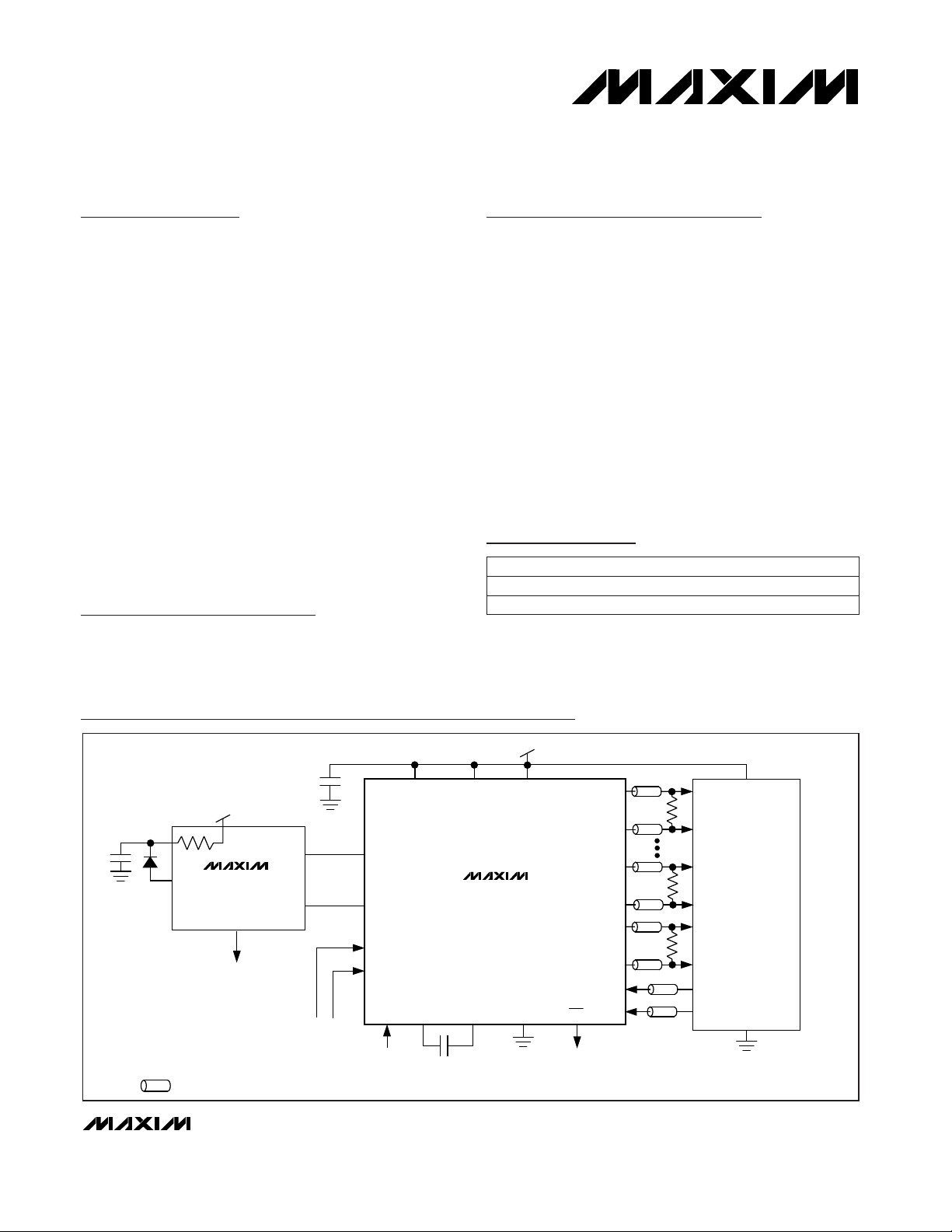
MAX3866
MAX3880
PRE/POSTAMPLIFIER
OVERHEAD
TERMINATION
100Ω*
*REQUIRED ONLY IF OVERHEAD CIRCUIT DOES NOT INCLUDE INTERNAL INPUT TERMINATION.
THIS SYMBOL REPRESENTS A TRANSMISSION LINE OF CHARACTERISTIC IMPEDANCE Z
0
= 50Ω.
V
CC
+3.3V
PHADJ-
V
CC
LOL
GNDFIL-
FIL+
SIS
TTL TTL
SDI+
OUT+
V
CC
IN+
FIL
OUT-
LOP
TTL
SDI-
SLBI-
SLBI+
SYSTEM
LOOPBACK
SYNC+
SYNC-
PD15+
PD15-
100Ω*
PD0+
PD0-
100Ω*
PCLK+
PCLK-
PHADJ+
0.01µF
+3.3V
C
F
1µF
Typical Application Circuit
19-1467; Rev 2; 12/05
PART
MAX3880ECB -40°C to +85°C
TEMP. RANGE PIN-PACKAGE
64 TQFP-EP*
Ordering Information
*Exposed pad
+Denotes lead-free package.
Pin Configuration appears at end of data sheet.
For free samples and the latest literature, visit www.maxim-ic.com or phone 1-800-998-8800.
For small orders, phone 1-800-835-8769.
MAX3880ECB+ -40°C to +85°C 64 TQFP-EP*
Page 2
MAX3880
+3.3V, 2.488Gbps, SDH/SONET
1:16 Deserializer with Clock Recovery
2 _______________________________________________________________________________________
ABSOLUTE MAXIMUM RATINGS
DC ELECTRICAL CHARACTERISTICS
(VCC= +3.0V to +3.6V, differential loads = 100Ω ±1%, TA= -40°C to +85°C, unless otherwise noted. Typical values are at
V
CC
= +3.3V, TA= +25°C.)
Stresses beyond those listed under “Absolute Maximum Ratings” may cause permanent damage to the device. These are stress ratings only, and functional
operation of the device at these or any other conditions beyond those indicated in the operational sections of the specifications is not implied. Exposure to
absolute maximum rating conditions for extended periods may affect device reliability.
Positive Supply Voltage (VCC)...............................-0.5V to +7.0V
Input Voltage Level (SDI+, SDI-, SLBI+, SLBI-,
SYNC+, SYNC-)........................... (V
CC
- 0.5V) to (VCC+ 0.5V)
Input Current Level (SDI+, SDI-, SLBI+, SLBI-)................±10mA
Voltage at LOL, SIS, PHADJ+, PHADJ-,
FIL+, FIL- .................................................-0.5V to (V
CC
+ 0.5V)
Output Current LVDS Outputs ............................................10mA
Continuous Power Dissipation (T
A
= +85°C)
TQFP (derate 33.3mW/°C above +85°C).......................1.44W
Operating Temperature Range ...........................-40°C to +85°C
Storage Temperature Range .............................-55°C to +150°C
Lead Temperature (soldering, 10s) .................................+300°C
Figure 1
Common-mode voltage = 50mV
Figure 2
Differential input voltage = 100mV
CONDITIONS
%±2.5 ±10
∆R
O
Change in Magnitude of SingleEnded Output Resistance for
Complementary Outputs
Ω40 95 140R
O
Single-Ended Output
Resistance
mV±25
∆V
OS
Change in Magnitude of Output
Offset Voltage for
Complementary States
V1.125 1.275V
OS
Output Offset Voltage
mV±25
∆|VOD|
Change in Magnitude of
Differential Output Voltage for
Complementary States
mV250 400
|
V
OD
|
Differential Output Voltage
V0.925V
OL
Output Low Voltage
mVp-p50 800V
ID
Differential Input Voltage
mA275 380I
CC
Supply Current
V1.475V
OH
Output High Voltage
Ω85 100 115R
IN
Differential Input Resistance
mV78V
HYST
Threshold Hysteresis
mV-100 100V
IDTH
Differential Input Threshold
VVCC- 0.4 VCC+ 0.2V
IS
Single-Ended Input Voltage
Ω50R
IN
Input Termination to Vcc
V0 2.4V
I
Input Voltage Range
UNITSMIN TYP MAXSYMBOLPARAMETER
V0.8V
IL
Input Low Voltage
V2.0V
IH
Input High Voltage
V2.4 V
CC
V
OH
Output High Voltage
µA-10 +10Input Current
V0.4V
OL
Output Low Voltage
SERIAL DATA INPUTS (SDI±, SLBI±)
LVDS INPUTS AND OUTPUTS (SYNC±, PCLK±, PD_±)
TTL INPUTS AND OUTPUTS (SIS, LOL)
Page 3
MAX3880
+3.3V, 2.488Gbps, SDH/SONET
1:16 Deserializer with Clock Recovery
_______________________________________________________________________________________ 3
AC ELECTRICAL CHARACTERISTICS
(VCC= +3.0V to +3.6V, differential loads = 100Ω ±1%, TA= -40°C to +85°C, unless otherwise noted. Typical values are at
V
CC
= +3.3V, TA= +25°C.) (Note 1)
Note 1: AC characteristics are guaranteed by design and characterization.
Note 2: At jitter frequencies <70kHz, the jitter tolerance characteristics exceed the ITU/Bellcore specifications. The low-frequency
jitter tolerance outperforms the instrument’s measurement capability.
Figure 5
100kHz to 2.5GHz
f = 10MHz
f = 70kHz (Note 2)
f = 100kHz
f = 1MHz
2.5GHz to 4.0GHz
CONDITIONS
dB
-11
Input Return Loss (SDI±, SLBI±)
ps200 450 900t
CLK-Q
Parallel Clock-to-Data Output
Delay
Mbps155.52
Gbps2.488SDISerial Data Rate
Parallel Output Data Rate
-18
Bits>2,000
Tolerated Consecutive Identical
Digits
UIp-p
0.28 0.46
Jitter Tolerance
2.31 3.3
1.74 2.41
0.38 0.57
UNITSMIN TYP MAXSYMBOLPARAMETER
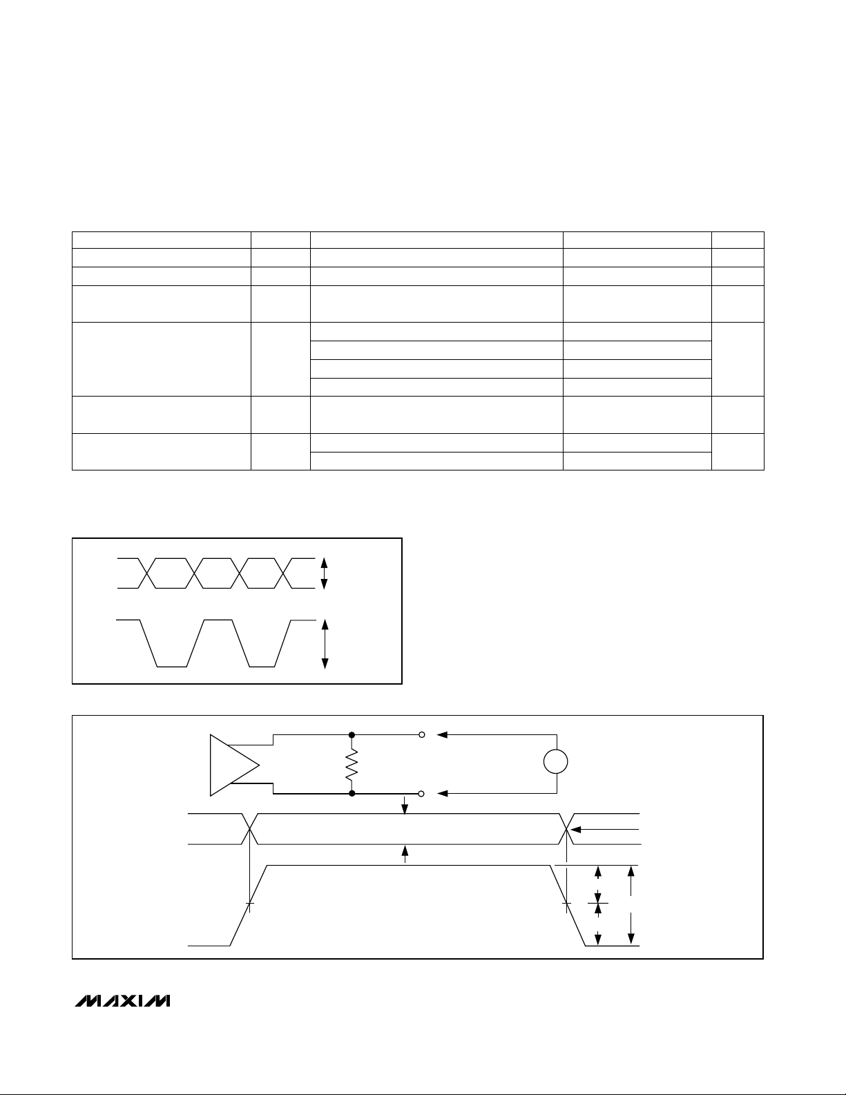
Figure 1. Input Amplitude
Figure 2. Driver Output Levels
SDI+
SDI-
25mV MIN
400mV MAX
(SDI+) - (SDI-)
V
PD-
SINGLE-ENDED OUTPUT
V
PD+
- V
V
PD+
PD-
DIFFERENTIAL OUTPUT
50mVp-p MIN
V
ID
800mVp-p MAX
PD+
V
= 100Ω
R
D
PD-
0V (DIFF)
L
V
|
OD|
V
OD
V
OH
V
OS
V
OL
+V
OD
0V
V
= V
PD+
- V
PD-
OD, p-p
-V
OD
Page 4
MAX3880
+3.3V, 2.488Gbps, SDH/SONET
1:16 Deserializer with Clock Recovery
4 _______________________________________________________________________________________
0
10 1,000100
JITTER TOLERANCE vs. INPUT VOLTAGE
0.3
0.1
0.6
0.4
0.8
0.2
0.7
0.5
MAX3880-04
INPUT VOLTAGE (mVp-p)
JITTER TOLERANCE (UIp-p)
JITTER FREQUENCY = 1MHz
JITTER FREQUENCY
= 5MHz
SONET SPEC
10
-10
10
-8
10
-9
10
-6
10
-7
10
-4
10
-5
10
-3
6.0 7.06.5 7.5 8.0 8.5 9.0 9.5 10.0
BIT ERROR RATE vs. INPUT VOLTAGE
MAX3880-05
INPUT VOLTAGE (mVp-p)
BIT ERROR RATE
200
300
400
600
500
700
-50 0-25 25 50 75 100
PARALLEL CLOCK TO DATA OUTPUT
PROPAGATION DELAY vs. TEMPERATURE
MAX3880-06
TEMPERATURE (°C)
PCLK TO DATA OUTPUT PROPAGATION DELAY (ps)
Typical Operating Characteristics
(VCC= +3.3V, TA = +25°C, unless otherwise noted.)
1.64ns/div
DATA
CLOCK
RECOVERED DATA AND CLOCK
(DIFFERENTIAL OUTPUT)
MAX3880-01
2
23
- 1 PATTERN
240
250
260
270
280
290
300
-50 -25 0 25 50 75 100
SUPPLY CURRENT vs. TEMPERATURE
MAX3880-02
TEMPERATURE (°C)
SUPPLY CURRENT (mA)
VCC = 3.6V
VCC = 3.0V
10
0.1
10 1,000 10,000
JITTER TOLERANCE
1
MAX3880-03
JITTER FREQUENCY (kHz)
INPUT JITTER (UIPp-p)
100
Page 5

MAX3880
+3.3V, 2.488Gbps, SDH/SONET
1:16 Deserializer with Clock Recovery
_______________________________________________________________________________________ 5
NAME FUNCTION
1, 17, 25, 33,
41, 49, 56,
62, 64
GND Ground
PIN
Pin Description
2 FIL+ Positive Filter Input. PLL loop filter connection. Connect a 1.0µF capacitor between FIL+ and FIL-.
3 FIL- Negative Filter Input. PLL loop filter connection. Connect a 1.0µF capacitor between FIL+ and FIL-.
4, 7, 10, 13,
24, 32, 40,
48, 57
V
CC
+3.3V Supply Voltage
5 PHADJ+
Positive Phase-Adjust Input. Used to optimally align internal PLL phase. Connect to VCCif not
used.
6 PHADJ-
Negative Phase-Adjust Input. Used to optimally align internal PLL phase. Connect to VCCif not
used.
8 SDI+ Positive Serial Data Input. 2.488Gbps data stream.
9 SDI- Negative Serial Data Input. 2.488Gbps data stream.
11 SLBI+ Positive System Loopback Input. 2.488Gbps data stream.
12 SLBI- Negative System Loopback Input. 2.488Gbps data stream.
14 SIS
Signal Input Selection. TTL low for normal data input (SDI). TTL high for system loopback input
(SLBI).
15 SYNC-
Negative Synchronizing Pulse LVDS Input. Pulse the SYNC signal high for at least four serial-data
bit periods (1.6ns) to shift the data alignment by dropping 1 bit.
16 SYNC+
Positive Synchronizing Pulse LVDS Input. Pulse the SYNC signal high for at least four serial-data
bit periods (1.6ns) to shift the data alignment by dropping 1 bit.
18 PCLK- Negative Parallel Clock LVDS Output
19 PCLK+ Positive Parallel Clock LVDS Output
20, 22, 26,
28, 30, 34,
36, 38, 42,
44, 46, 50,
52, 54, 58, 60
PD0- to
PD15-
Negative Parallel Data LVDS Outputs. Data is updated on the negative transition of the PCLK
signal (Figure 5).
21, 23, 27,
29, 31, 35,
37, 39, 43,
45, 47, 51,
53, 55, 59, 61
PD0+ to
PD15+
Positive Parallel Data LVDS Outputs. Data is updated on the negative transition of the PCLK
signal (Figure 5).
63
LOL
Loss-of-Lock Output. PLL loss-of-lock monitor, TTL active low (internal 10kΩ pull-up resistor). The
LOL monitor is valid only when a data stream is present on the inputs to the MAX3880.
EP Exposed Pad
Ground. This must be soldered to a circuit board for proper thermal performance (see Package
Information).
Page 6

MAX3880
+3.3V, 2.488Gbps, SDH/SONET
1:16 Deserializer with Clock Recovery
6 _______________________________________________________________________________________
MAX3880
SDI+
AMP
LVDS
PD15+
PD15-
LVDS
LVDS
LVDS
LVDS
LOL
TTL
100Ω
50Ω
50Ω
MUX
PHASE &
FREQUENCY
DETECTOR
SDI-
SLBI+
AMP
SLBI-
SIS
V
CC
V
CC
SYNC-
SYNC+
LOOP
FILTER
VCO
16-BIT
DEMULTIPLEXER
D
Q
CK
PHADJ+ PHADJ- FIL+ FIL-
CLOCK
DIVIDER
PD1+
PD1-
PD0+
PD0-
PCLK+
PCLK-
Figure 3. MAX3880 Functional Diagram
Detailed Description
The MAX3880 deserializer with clock recovery converts
2.488Gbps serial data to 16-bit-wide, 155Mbps parallel
data. The device combines a fully integrated phaselocked loop (PLL), input amplifier, data retiming block,
16-bit demultiplexer, clock divider, and LVDS output
buffer (Figure 3). The PLL consists of a phase/frequency detector (PFD), a loop filter, and a voltage-controlled
oscillator (VCO). The MAX3880 is designed to deliver
the best combination of jitter performance and power
dissipation by using a fully differential signal architecture and low-noise design techniques. The PLL recovers the serial clock from the serial input data stream.
The demultiplexer generates a 16-bit-wide 155Mbps
parallel data output.
The synchronization inputs (SYNC+, SYNC-) realign the
output data word. Realignment is guaranteed to occur
within two complete PCLK cycles of the SYNC signal’s
positive transition. During synchronization, the first
incoming bit of data during that PCLK cycle is
Page 7

MAX3880
+3.3V, 2.488Gbps, SDH/SONET
1:16 Deserializer with Clock Recovery
_______________________________________________________________________________________ 7
dropped, shifting the alignment between PCLK and
data by 1 bit. The SYNC signal must be at least four
serial bit periods wide (4 x 402ps). See Figure 4 for the
timing diagram and Figure 5 for the timing parameters
diagram.
Input Amplifier
The input amplifiers on both the main data and system
loopback accept a differential input amplitude from
50mVp-p to 800mVp-p. The bit error rate (BER) is better than 1 x 10
-10
for input signals as small as 9.5mVpp, although the jitter tolerance performance will be
degraded. For interfacing with PECL signal levels, see
Applications Information.
Phase Detector
The phase detector in the MAX3880 produces a voltage proportional to the phase difference between the
incoming data and the internal clock. Because of its
feedback nature, the PLL drives the error voltage to
zero, aligning the recovered clock to the center of the
incoming data eye for retiming. The external phase
adjust pins (PHADJ+, PHADJ-) allow the user to vary
the internal phase alignment.
Frequency Detector
The digital frequency detector (FD) aids frequency
acquisition during start-up conditions. The frequency
difference between the received data and the VCO
clock is derived by sampling the in-phase and quadrature VCO outputs on both edges of the data input signal. Depending on the polarity of the frequency
difference, the FD drives the VCO until the frequency
difference is reduced to zero. Once frequency acquisition is complete, the FD returns to a neutral state. False
locking is completely eliminated by this digital frequency detector.
Loop Filter and VCO
The phase detector and frequency detector outputs are
summed into the loop filter. A 1.0µF capacitor, CF, is
required to set the PLL damping ratio.
The loop filter output controls the on-chip LC VCO running at 2.488GHz. The VCO provides low phase noise
and is trimmed to the correct frequency.
Loss-of-Lock Monitor
A loss-of-lock (LOL) monitor is included in the
MAX3880 frequency detector. A loss-of-lock condition
is signaled immediately with a TTL low. When the PLL is
frequency-locked, LOL switches to TTL high in approximately 800ns.
Note that the LOL monitor is only valid when a data
stream is present on the inputs to the MAX3880. As a
result, LOL does not detect a loss-of-power condition
resulting from a loss of the incoming signal.
SDI
SYNC
PCLK
D0
D15 D14 D13
D16 D32 D48
1 BIT HAS SLIPPED
IN THIS TIME SLICE
D65
(LSB) PD0
D1 D17 D33 D49 D66
PD1
D15
(MSB)
TRANSMITTED FIRST
D31 D47 D64 D80
PD15
•
•
•
Figure 4. Timing Diagram
Page 8

MAX3880
+3.3V, 2.488Gbps, SDH/SONET
1:16 Deserializer with Clock Recovery
8 _______________________________________________________________________________________
Low-Voltage Differential-Signal (LVDS)
Inputs and Outputs
The MAX3880 features LVDS inputs and outputs for
interfacing with high-speed digital circuitry. The LVDS
standard is based on the IEEE 1596.3 LVDS specification. This technology uses 500mVp-p to 800mVp-p differential low-voltage swings to achieve fast transition
times, minimize power dissipation, and improve noise
immunity. For proper operation, the parallel clock and
data LVDS outputs (PCLK+, PCLK-, PD_+, PD_-)
require 100Ω differential DC termination between the
positive and negative outputs. Do not terminate these
outputs to ground. The synchronization LVDS inputs
(SYNC+, SYNC-) are internally terminated with 100Ω
differential input resistance and therefore do not require
external termination.
Design Procedure
Jitter Tolerance and Input
Sensitivity Trade-Offs
When the received data amplitude is higher than
50mVp-p, the MAX3880 provides a typical jitter tolerance of 0.46 UI at jitter frequencies greater than
10MHz. The SDH/SONET jitter tolerance specification is
0.15UI, leaving a jitter allowance of 0.31UI for receiver
preamplifier and postamplifier design.
The BER is better than 1 x 10
-10
for input signals
greater than 9.5mVp-p. At 25mVp-p, jitter tolerance will
be degraded, but will still be above the SDH/SONET
requirement. Trade-offs can be made between jitter tolerance and input sensitivity according to the specific
application. See the Typical Operating Characteristics
for Jitter Tolerance and BER vs. Input Voltage graphs.
Applications Information
Consecutive Identical Digits (CIDs)
The MAX3880 has a low phase and frequency drift in
the absence of data transitions. As a result, long runs of
consecutive zeros and ones can be tolerated while
maintaining a BER of 1 x 10
-10
. The CID tolerance is
tested using a 2
13
- 1 pseudorandom bit stream
(PRBS), substituting a long run of zeros to simulate the
worst case. A CID tolerance of greater than 2,000 bits
is typical.
Phase Adjust
The internal clock is aligned to the center of the data
eye. For specific applications, this sampling position
can be shifted using the PHADJ inputs to optimize BER
performance. The PHADJ inputs operate with differential input voltages up to ±1.5V. A simple resistor-divider
with a bypass capacitor is sufficient to set these levels
(Figure 6). When the PHADJ inputs are not used, they
should be tied directly to VCC.
System Loopback
The MAX3880 is designed to allow system loopback
testing. The user can connect a serializer output
(MAX3890) in a transceiver directly to the SLBI+ and
SLBI- inputs of the MAX3880 for system diagnostics. To
select the SLBI± inputs, apply a TTL logic high to the
SIS pin.
PCLK
PD0–PD15
NOTE: SIGNALS SHOWN ARE DIFFERENTIAL. FOR EXAMPLE, PCLK = (PCLK+) - (PCLK-).
t
CLK-Q
Figure 5. Timing Parameters
MAX3880
PHADJ+ (PIN 5)
PHADJ- (PIN 6)
3.3V
Figure 6. Phase-Adjust Resistor-Divider
Page 9

MAX3880
+3.3V, 2.488Gbps, SDH/SONET
1:16 Deserializer with Clock Recovery
_______________________________________________________________________________________ 9
Interfacing with PECL Input Levels
When interfacing with differential PECL input levels, it is
important to attenuate the signal while still maintaining
50Ω termination (Figure 7). AC-coupling is also
required to maintain the input common-mode level.
Layout Techniques
For best performance, use good high-frequency layout
techniques. Filter voltage supplies, keep ground connections short, and use multiple vias where possible.
Use controlled impedance transmission lines to interface with the MAX3880 high-speed inputs and outputs.
Power-supply decoupling should be placed as close to
VCCas possible. To reduce feedthrough, take care to
isolate the input signals from the output signals.
MAX3880
50Ω
50Ω
V
CC
100Ω
PECL
LEVELS
SDI+
25Ω
25Ω
0.1µF
0.1µF
SDI-
Figure 7. Interfacing with PECL Input Levels
Chip Information
TRANSISTOR COUNT: 4102
Page 10

MAX3880
+3.3V, 2.488Gbps, SDH/SONET
1:16 Deserializer with Clock Recovery
10 ______________________________________________________________________________________
Pin Configuration
PD13-
PD13+
GND
VCCPD14-
PD14+
GND
PD11-
PD11+
PD12-
PD12+
PD15-
PD15+
GND
LOL
GND
SLBI+
V
CC
SDI-
SDI+
V
CC
PHADJ-
SYNC+
SYNC-
SIS
V
CC
SLBI-
PHADJ+
V
CC
FIL-
FIL+
GND
PCLK-
PCLK+
PD0-
PD0+
PD1-
PD1+
V
CC
GND
PD2-
PD2+
PD3-
PD3+
PD4-
PD4+
V
CC
GND
PD10+
TOP VIEW
PD10-
PD9+
PD9-
PD8+
PD8-
GND
V
CC
PD7+
PD7-
PD6+
PD6-
PD5+
PD5-
GND
V
CC
TQFP-EP
5859606162 5455565763
38
39
40
41
42
43
44
45
46
47
5253
49
5051
33
34
35
36
37
48
64
2322212019 2726252418 2928 32313017
11
10
9
8
7
6
5
4
3
2
16
15
14
13
12
1
MAX3880
Page 11

MAX3880
+3.3V, 2.488Gbps, SDH/SONET
1:16 Deserializer with Clock Recovery
______________________________________________________________________________________ 11
64L, TQFP.EPS
C
1
2
21-0084
PACKAGE OUTLINE,
64L TQFP, 10x10x1.0mm EP OPTION
Package Information
(The package drawing(s) in this data sheet may not reflect the most current specifications. For the latest package outline information
go to www.maxim-ic.com/packages
.)
Page 12

MAX3880
+3.3V, 2.488Gbps, SDH/SONET
1:16 Deserializer with Clock Recovery
Maxim cannot assume responsibility for use of any circuitry other than circuitry entirely embodied in a Maxim product. No circuit patent licenses are
implied. Maxim reserves the right to change the circuitry and specifications without notice at any time.
12 ____________________Maxim Integrated Products, 120 San Gabriel Drive, Sunnyvale, CA 94086 408-737-7600
© 2005 Maxim Integrated Products Printed USA is a registered trademark of Maxim Integrated Products, Inc.
C
2
2
21-0084
PACKAGE OUTLINE,
64L TQFP, 10x10x1.0mm EP OPTION
Package Information (continued)
(The package drawing(s) in this data sheet may not reflect the most current specifications. For the latest package outline information
go to www.maxim-ic.com/packages
.)
 Loading...