

General Description
The MAX3867 is a complete, single +3.3V laser driver
for SDH/SONET applications up to 2.5Gbps. The
device accepts differential PECL data and clock inputs
and provides bias and modulation currents for driving a
laser. The synchronizing input latch can be bypassed if
a clock signal is not available.
An automatic power control (APC) feedback loop is
incorporated to maintain a constant average optical
power over temperature and lifetime. The wide modulation current range of 5mA to 60mA and bias current of
1mA to 100mA are easy to program, making this product ideal for use in various SDH/SONET applications.
The MAX3867 also provides enable control, a programmable slow-start circuit to set the laser turn-on delay,
and a failure-monitor output to indicate when the APC
loop is unable to maintain the average optical power.
The MAX3867 is available in a small 48-pin TQFP package as well as dice.
Applications
SONET/SDH Transmission Systems
Add/Drop Multiplexers
Digital Cross-Connects
Section Regenerators
2.5Gbps Optical Transmitters
Features
♦ Single +3.3V or +5V Power Supply
♦ 62mA Supply Current at +3.3V
♦ Programmable Modulation Current from
5mA to 60mA
♦ Programmable Bias Current from 1mA to 100mA
♦ Rise/Fall Time < 90ps
♦ Automatic Average Power Control with Failure
Monitor
♦ Complies with ANSI, ITU, and Bellcore
SDH/SONET Specifications
♦ Enable Control
*
Dice are designed to operate over this range, but are tested and
guaranteed at TA= +25°C only. Contact factory for availability.
Ordering Information
MAX3867
+3.3V, 2.5Gbps SDH/SONET Laser Driver
with Automatic Power Control
________________________________________________________________
Maxim Integrated Products
1
EVALUATION KIT
AVAILABLE
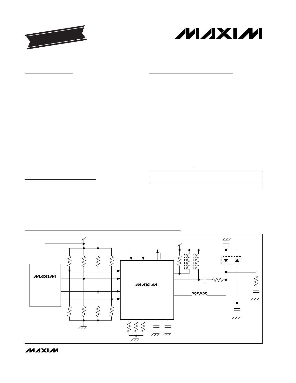
124Ω 124Ω
SERIALIZER
WITH
CLOCK GEN.
124Ω
20Ω
LD
25Ω
+3.3V
+3.3V
0.056µF
1000pF
BIASMAX
LATCH
ENABLE
FAIL
MODSET
APCSET
APCFILT
CLK-
CLK+
DATA-
DATA+
*FERRITE
BEAD
OUT+
BIAS
MD
OUT-
CAPC
124Ω
84.5Ω 84.5Ω 84.5Ω84.5Ω
MAX3867
MAX3890
Typical Operating Circuit
19-4769; Rev 0a; 9/98
Pin Configuration appears at end of data sheet.
PART
MAX3867ECM
MAX3867E/D -40°C to +85°C
-40°C to +85°C
TEMP. RANGE PIN-PACKAGE
48 TQFP
Dice*
For free samples & the latest literature: http://www.maxim-ic.com, or phone 1-800-998-8800.
For small orders, phone 1-800-835-8769.
MAX3867
+3.3V, 2.5Gbps SDH/SONET Laser Driver
with Automatic Power Control
2 _______________________________________________________________________________________
IMD= 1mA
IMD= 18µA
90
ENABLE = low (Note 4)
APC open loop, I
BIAS
= 1mA
(Note 3)
900
(Note 2)
(Note 5)
Sourcing 50µA
(Note 6)
APC open loop, I
BIAS
= 100mA
APC open loop
Figure 1
PECL compatible
Sinking 100µA
CONDITIONS
%
-15 15
Monitor-Diode Bias Absolute
Accuracy
ppm/°C
-480 50 480
Monitor-Diode Bias Setpoint
Stability
µA
18 1000
I
MD
Monitor-Diode DC Current
Range
V
1.5
Monitor-Diode Reverse Bias
Voltage
V
0.1 0.44
TTL Output Low Voltage FAIL
µA
100
I
BIAS-OFF
Bias Off Current
mA
1 100
I
BIAS
mA
62 105
I
CC
Supply Current
Bias Current Range
V
2.4 VCC- 0.3 V
CC
TTL Output High Voltage FAIL
V
0.8
TTL Input Low Voltage
(ENABLE, LATCH)
V
2.0
TTL Input High Voltage
(ENABLE, LATCH)
µA
-1 10
I
IN
Clock and Data Input Current
ppm/°C
230
Bias-Current Stability
%
-15 15
(Note 5)Bias-Current Absolute Accuracy
mVp-p
200 1600
V
ID
Differential Input Voltage
V
VCC- VCC- VCC-
1.49 1.32 V
ID
/4
V
ICM
Common-Mode Input Voltage
UNITSMIN TYP MAXSYMBOLPARAMETER
DC ELECTRICAL CHARACTERISTICS
(VCC= +3.14V to +5.5V, TA= -40°C to +85°C. Typical values are at VCC= +3.3V, I
MOD
= 30mA, I
BIAS
= 60mA, and TA= +25°C,
unless otherwise noted.) (Note 1)
Stresses beyond those listed under “Absolute Maximum Ratings” may cause permanent damage to the device. These are stress ratings only, and functional
operation of the device at these or any other conditions beyond those indicated in the operational sections of the specifications is not implied. Exposure to
absolute maximum rating conditions for extended periods may affect device reliability.
Note 1: Characteristics at -40°C guaranteed by design and characterization. Dice are tested at TA= +25°C only.
Note 2: Tested at R
MODSET
= 2.49kΩ, R
BIASMAX
= 1.69kΩ, excluding I
BIAS
and I
MOD
.
Note 3: Voltage on BIAS pin is (V
CC
- 1.6V).
Note 4: Both the bias and modulation currents will be switched off if any of the current set pins are grounded.
Note 5: Accuracy refers to part-to-part variation.
Note 6: Assuming that the laser to monitor-diode transfer function does not change with temperature.
Supply Voltage, V
CC
............................................. -0.5V to +7.0V
Current into BIAS ...........................................-20mA to +150mA
Current into OUT+, OUT-................................-20mA to +100mA
Current into MD.....................................................-5mA to +5mA
Voltage at DATA+, DATA-, CLK+, CLK-,
ENABLE, LATCH, FAIL, SLWSTRT.........-0.5V to (V
CC
+ 0.5V)
Voltage at APCFILT, CAPC, MODSET,
BIASMAX, APCSET ...........................................-0.5V to +3.0V
Voltage at OUT+, OUT-.............................+1.5V to (V
CC
+ 1.5V)
Voltage at BIAS.........................................+1.0V to (V
CC
+ 0.5V)
Current into FAIL ...............................................-10mA to +30mA
Continuous Power Dissipation (T
A
= +85°C)
TQFP (derate 20.8mW/°C above +85°C)...................1354mW
Storage Temperature Range.............................-65°C to +165°C
Operating Junction Temperature Range...........-55°C to +150°C
Processing Temperature (die).........................................+400°C
Lead Temperature (soldering, 10sec).............................+300°C
ABSOLUTE MAXIMUM RATINGS
MAX3867
+3.3V, 2.5Gbps SDH/SONET Laser Driver
with Automatic Power Control
_______________________________________________________________________________________ 3
AC ELECTRICAL CHARACTERISTICS
(V
CC
= +3.14V to +5.5V, load as shown in Figure 2, TA= -40°C to +85°C. Typical values are at VCC= +3.3V, I
MOD
= 30mA, and TA=
+25°C.) (Note 7)
Note 7: AC characteristics are guaranteed by design and characterization.
Note 8: Measured with 622Mbps 0-1 pattern, LATCH = high.
Note 9: PWD = (wider pulse - narrower pulse) / 2.
Note 10: See
Typical Operating Characteristics
for worst-case distribution.
I
MOD
= 5mA
250
79
LATCH = high, Figure 3
LATCH = high, Figure 3
20% to 80% (Note 8)
ps
69
(Note 8)
20% to 80% (Note 8)
ENABLE = low (Note 4)
I
MOD
= 60mA
(Note 6)
Jitter BW = 12kHz to 20MHz, 0-1 pattern
(Notes 8, 9)
CONDITIONS
t
R
Output Rise Time ps
ps
p-p
720
Jitter Generation
ps
950
PWDPulse-Width Distortion
mA
560
I
MOD
Modulation-Current Range
ps
100
t
H
ps
100
t
SU
Input Latch Setup Time
Input Latch Hold Time
bits
80
Maximum Consecutive Identical
Digits
ns
250
Enable/Start-Up Delay
%
±15
Output Aberrations
79
t
F
Output Fall Time
µA
200
I
MOD-OFF
Modulation-Off Current
ppm/°C
-480 -50 480
Modulation-Current Stability
%
-15 15
Modulation-Current Absolute
Accuracy
88 (Note 10)
UNITSMIN TYP MAXSYMBOLPARAMETER
MAX3867ECM
MAX3867C/D
MAX3867ECM
MAX3867C/D
MAX3867
+3.3V, 2.5Gbps SDH/SONET Laser Driver
with Automatic Power Control
4 _______________________________________________________________________________________
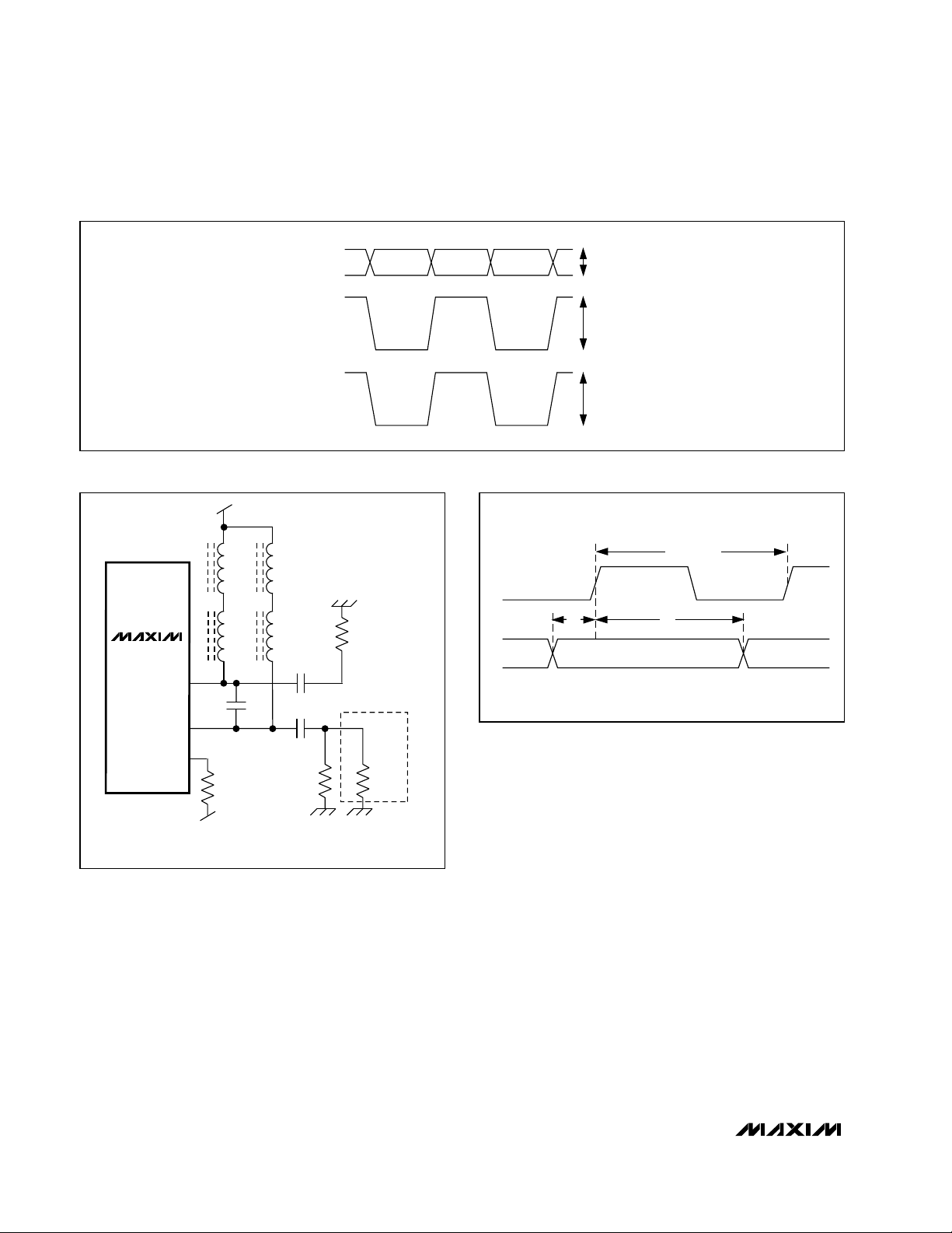
DATA+
DATA-
(DATA+) - (DATA-)
I
OUT
+
100mV MIN
800mV MAX
200mVp-p MIN
1600mVp-p MAX
I
MOD
Figure 1. Required Input Signal and Output Polarity
CLK
DATA
t
CLK
= 402ps
t
SU
t
H
Figure 3. Setup/Hold Time Definition
0.056µF
0.5pF
*
* TO COMPENSATE PACKAGE LEADS, NOT USED FOR DIE.
OUT+
BIAS
OUT-
A
B
A
A, B ARE SMD FERRITE BEADS
B = BLM11A601S MURATA ELECTRONICS
A = BLM21A102S MURATA ELECTRONICS
B
V
CC
50Ω
15Ω
OSCILLOSCOPE
50Ω
25Ω
0.056µF
V
CC
MAX3867
Figure 2. Output Termination for Characterization
MAX3867
+3.3V, 2.5Gbps SDH/SONET Laser Driver
with Automatic Power Control
_______________________________________________________________________________________
5
26mV
/div
50ps/div
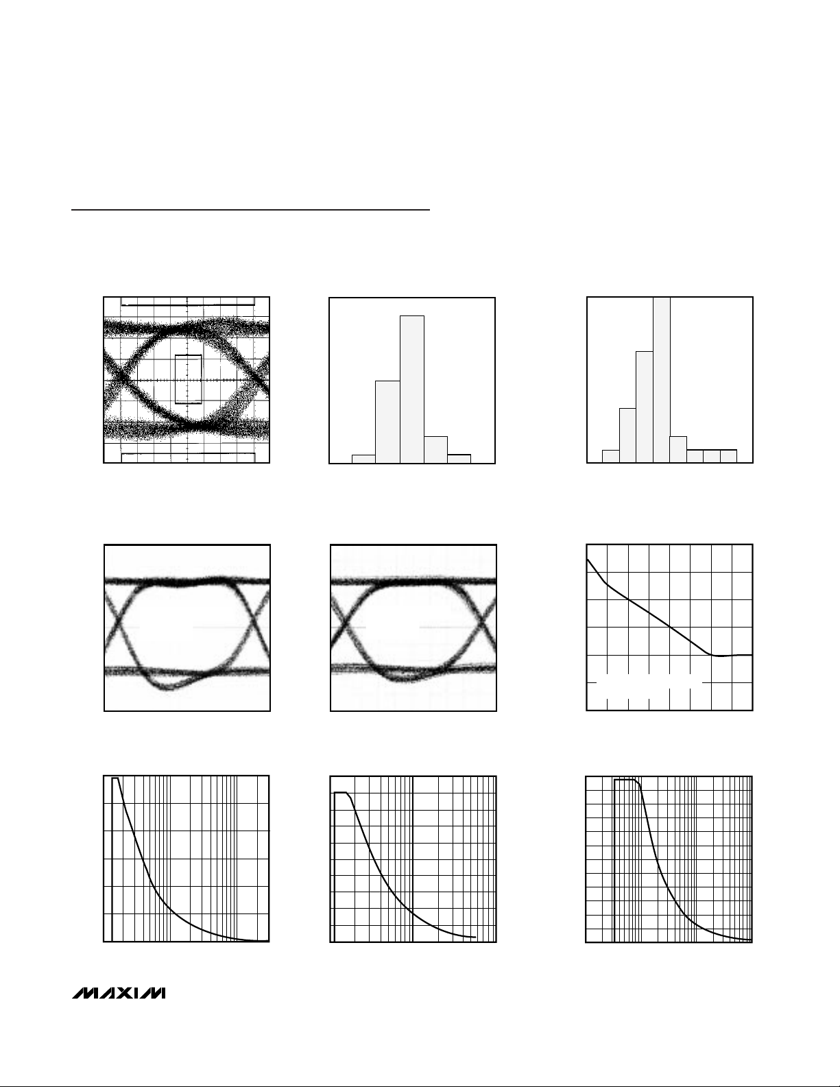
ELECTRICAL EYE DIAGRAM
MAX3867-04a
PATTERN = 213 - 1 + 80 CID
I
MOD
= 30mA
48-TQFP
0.010
0.012
0.014
0.016
0.018
0.020
0.022
41811 25 32 39 46 53 60
RANDOM JITTER vs. I
MOD
MAX3867 toc05
I
(mA)
RANDOM JITTER (UIp-p)
JITTER BW = 12kHz to 20MHz
1-0 PATTERN
55mV
/div
50ps/div
ELECTRICAL EYE DIAGRAM
MAX3867-05a
PATTERN = 213 - 1 + 80 CID
I
MOD
= 60mA
48-TQFP
120
0
110
100
300
I
BIASMAX
vs. R
BIASMAX
MAX3867-06
R
BIASMAX
(kΩ)
I
BIASMAX
(mA)
40
80
100
20
60
100
0
1 10 100
I
MOD
vs. R
MODSET
20
10
MAX3867-07
R
MODSET
(kΩ)
I
MOD
(mA)
40
30
60
70
50
80
90
1.2
0
0.1 1 10 100
IMD vs. R
APCSET
0.4
MAX3867-08
R
APCSET
(kΩ)
I
MD
(mA)
0.6
0.8
1.0
1.1
0.3
0.2
0.1
0.5
0.7
0.9
Typical Operating Characteristics
(V
CC
= +3.3V, load as shown in Figure 2, TA= +25°C, unless otherwise noted.)
EYE DIAGRAM
(2.488Gbps, 1300nm FP LASER,
1.87GHz FILTER, 48-TQFP)
MAX3867-01
50ps/div
0
20
10
40
30
50
60
80 88
48-TQFP
I
MOD
= 30mA
MEAN = 88ps
σ = 3.0ps
92 9684100
TYPICAL DISTRIBUTION OF FALL TIME
MAX3867-02a
FALL TIME (ps)
PERCENT IN UNITS (%)
0
20
15
10
5
30
25
40
35
106 108 112
48-TQFP
I
MOD
= 30mA
VCC = +3.14V
T
A
= +85°C
MEAN = 111.6ps
σ = 2.9ps
114 116 118
110
120 122
DISTRIBUTION OF FALL TIME
(WORST-CASE CONDITIONS)
MAX3867-03a
FALL TIME (ps)
PERCENT IN UNITS (%)
MAX3867
+3.3V, 2.5Gbps SDH/SONET Laser Driver
with Automatic Power Control
6 _______________________________________________________________________________________
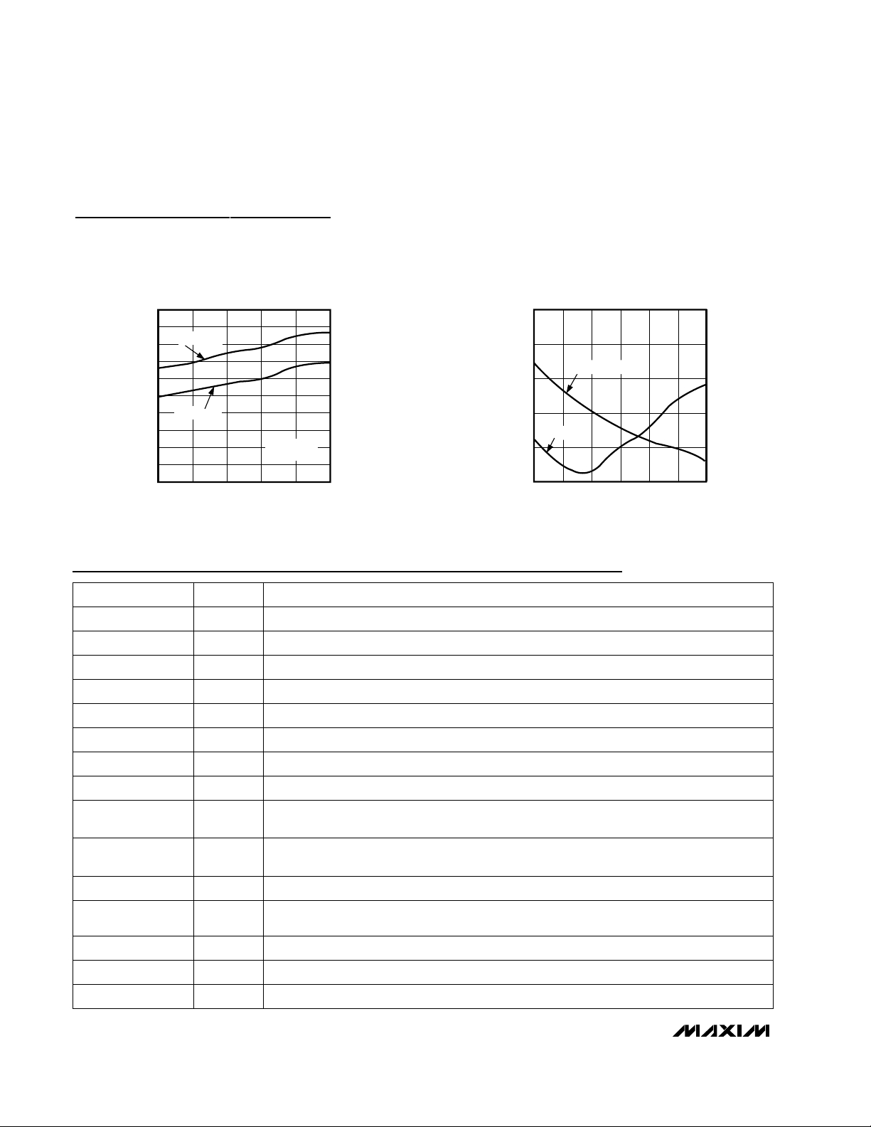
0
30
20
10
40
50
60
70
80
90
100
-40 10-15 35 60 85
SUPPLY CURRENT vs. TEMPERATURE
(EXCLUDE I
BIAS
, I
MOD
, 25Ω LOAD)
MAX3867-09
TEMPERATURE (°C)
I
CC
(mA)
VCC = +5V
VCC = +3.3V
I
MOD
= 30mA
I
BIAS
= 45mA
0.
5
15
10
20
25
52010 30 40 50 60
PULSE-WIDTH DISTORTION
vs. I
MOD
MAX3867-10
I
MOD
(mA)
PWD (ps)
V
CC
= +5V
VCC = +3.3V
Pin Description
Typical Operating Characteristics (continued)
(V
CC
= +3.3V, load as shown in Figure 2, TA= +25°C, unless otherwise noted.)
NAME FUNCTION
1, 42, 45 GND2 Ground for internal reference
2, 7, 12, 15, 16, GND1 Ground for digital circuits
PIN
3, 6, 8, 11, 18 VCC1 Power supply for digital circuits
4 DATA+ Positive PECL Data Input
13 LATCH TTL/CMOS Latch Input. High for latched data, low for direct data.
10 CLK- Negative PECL Clock Input. Leave unconnected if latch function is not used.
9 CLK+ Positive PECL Clock Input. Connect to VCCif latch function is not used.
5 DATA- Negative PECL Data Input
22 APCFILT Connect a capacitor (C
APCFILT
= 0.1µF) from this pad to ground to filter the APC noise.
21, 26, 28, 31, 39,
41, 43
N.C. No Connection. Leave unconnected.
19
FAIL
TTL/CMOS output. Indicates APC failure when low.
17 SLWSTRT
A capacitor from this pad to ground delays the turn-on time of laser bias and modulation
currents.
14 ENABLE
TTL/CMOS Enable Input. High for normal operation, low to disable laser bias and modulation
currents.
20, 23, 33 GND4 Ground for output circuitry
24, 27, 32 VCC4 Power Supply for output circuitry
_______________Detailed Description
The MAX3867 laser driver consists of two main parts: a
high-speed modulation driver and a laser-biasing block
with Automatic Power Control (APC). The circuit design
is optimized for both high-speed and low-voltage
(+3.3V) operation. To minimize the pattern-dependent
jitter of the input signal at speeds as high as 2.5Gbps,
the device accepts a differential PECL clock signal for
data retiming. When LATCH is high, the input data is
synchronized by the clock signal. When LATCH is low,
the input data is directly applied to the output stage.
The output stage is composed of a high-speed differential
pair and a programmable modulation current source.
Since the modulation output drives a maximum current
of 60mA into the laser with an edge speed of 100ps,
large transient voltage spikes can be generated due to
the parasitic inductance. These transients and the laser
forward voltage leave insufficient headroom for the
proper operation of the laser driver if the modulation
output is DC-coupled to the laser diode. To solve this
problem, the MAX3867’s modulation output is designed
to be AC-coupled to the cathode of a laser diode. An
external pull-up inductor is necessary to DC-bias the
modulation output at VCC. Such a configuration isolates
laser forward voltage from the output circuitry and
allows the output at OUT+ to swing above and below
the supply voltage VCC. A simplified functional diagram
is shown in Figure 4.
The MAX3867 modulation output is optimized for driving a 25Ω load; the minimum required voltage at OUT+
is 2.0V. Modulation current swings of 80mA are possible, but due to minimum power supply and jitter
requirements at 2.5Gbps, the specified maximum modulation current is limited to 60mA. To interface with the
laser diode, a damping resistor (RD) is required for
impedance matching. An RC shunt network is also necessary to compensate for the laser-diode parasitic
inductance, thereby improving the optical output aberrations and duty-cycle distortion.
At the data rate of 2.5Gbps, any capacitive load at the
cathode of a laser diode will degrade the optical output
performance. Since the BIAS output is directly connected
to the laser cathode, minimize the parasitic capacitance
associated with this pin by using an inductor to isolate the
BIAS pin from the laser cathode.
Automatic Power Control
To maintain constant average optical power, the
MAX3867 incorporates an APC loop to compensate for
the changes in laser threshold current over temperature
and lifetime. A back-facet photodiode mounted in the
MAX3867
+3.3V, 2.5Gbps SDH/SONET Laser Driver
with Automatic Power Control
_______________________________________________________________________________________ 7
NAME FUNCTIONPIN
25 BIAS Laser Bias Current Output
29 OUT+ Positive Modulation-Current Output. I
MOD
flows through this pad when input data is high.
37 VCC3 Power Supply for APC
34, 36, 40 GND3 Ground for APC
35 MD
Monitor Diode Input. Connect this pad to a monitor photodiode anode. A capacitor to ground
is required to filter high-speed AC monitor photocurrent.
30 OUT- Negative Modulation-Current Output. I
MOD
flows through this pad when input data is low.
48 VCC2 Power Supply for internal reference
47 BIASMAX
A resistor connected from this pad to ground sets the maximum bias current. The APC
function can subtract from this maximum value, but can not add to it.
46 MODSET A resistor connected from this pad to ground sets the desired modulation current.
44 APCSET
A resistor connected from this pad to ground sets the desired average optical power.
Connect 100kΩ from this pad to ground if APC is not used.
38 CAPC
A capacitor connected from this pad to ground controls the dominant pole of the APC feedback loop. (C
APC
= 0.1µF)
Pin Description (continued)

MAX3867
laser package is used to convert the optical power into
a photocurrent. The APC loop adjusts the laser bias
current so that the monitor current is matched to a reference current set by R
APCSET
. The time constant of
the APC loop is determined by an external capacitor
(C
APC
). To eliminate the pattern-dependent jitter associated with the APC loop-time constant, and to guarantee loop stability, the recommended value for C
APC
is
0.1µF.
When the APC loop is functioning, the maximum allow-
able bias current is set by an external resistor, R
BIASMAX
.
An APC failure flag (FAIL) is set low when the bias current
can no longer be adjusted to achieve the desired aver-
age optical power. To filter out the APC loop noise, use
an external capacitor at APCFILT with a recommended
value of 0.1µF.
APC closed-loop operation requires the user to set three
currents with external resistors connected between
ground and BIASMAX, MODSET, and APCSET. Detailed
guidelines for these resistor settings are described in
the
Design Procedure
section.
Open-Loop Operation
If necessary, the MAX3867 is fully operational without
APC. In this case, the laser current is directly set by two
external resistors connected from ground to BIASMAX
+3.3V, 2.5Gbps SDH/SONET Laser Driver
with Automatic Power Control
8 _______________________________________________________________________________________
LATCH
C
D
C
F
R
F
V
CC
1000pF
I
MD
R
APCSET
R
BIASMAX
R
MODSET
APCSET
CAPC
C
APC
BIASMAX
MD
MODSET
FAIL
BIAS
R
D
25Ω
I
MOD
I
BIAS
L
P
L
P
V
CC
MUX
DATA
CLK
0
1
ENABLE
OUT+
OUT-
DQ
172X
FAILURE
DETECTOR
40X
5X
MAX3867
Figure 4. Functional Diagram

and MODSET. See the
Design Procedure
section for
more details on open-loop operation.
Optional Data Input Latch
To minimize input data pattern-dependent jitter, the differential clock signal should be connected to the data
input latch, which is selected by an external LATCH
control. If LATCH is high, the input data is retimed by
the rising edge of CLK+. If LATCH is low, the input data
is directly connected to the output stage. When this
latch function is not used, connect CLK+ to VCCand
leave CLK- unconnected.
Enable Control
The MAX3867 incorporates a laser driver enable function. When ENABLE is low, both the bias and modulation
currents are off. The typical laser enable time is 250ns
and the typical disable time is 25ns.
Slow-Start
For laser safety reasons, the MAX3867 incorporates a
slow-start circuit which provides a programmable delay
time for enabling a laser diode. An external capacitor
(C
SLWSTRT
) connected from this pad to ground pro-
grams the delay by the equation:
t
ENABLE
≅ 100kΩ · (C
SLWSTRT
+ 2.5pF)
APC Failure Monitor
The MAX3867 provides an APC failure monitor
(TTL/CMOS) to indicate an APC loop tracking failure.
FAIL is set low when the APC loop can no longer adjust
the bias current to maintain the desired monitor current.
Short-Circuit Protection
The MAX3867 provides short-circuit protection for the
modulation, bias and monitor current sources. If either
BIASMAX, MODSET, or APCSET is shorted to ground,
the bias and modulation output will be turned off.
Design Procedure
When designing a laser transmitter, the optical output is
usually expressed in terms of average power and extinction ratio. Table 1 gives the relationships that are helpful
in converting between the optical average power and the
modulation current. These relationships are valid if the
average duty cycle of optical waveform is 50%
Programming the Modulation Current
For a given laser power P
AVE
, slope efficiency η, and
extinction ration re, the modulation current can be calculated by Table 1. Refer to the I
MOD
vs. R
MODSET
graph
in the
Typical Operating Characteristics
and select the
value of R
MODSET
that corresponds to the required cur-
rent at +25°C.
Programming the Bias Current
When using the MAX3867 in open-loop operation, the
bias current is determined by the R
BIASMAX
resistor. To
select this resistor, determine the required bias current
at +25°C. Refer to the I
BIASMAX
vs. R
BIASMAX
graph in
the
Typical Operating Characteristics
and select the
value of R
BIASMAX
that corresponds to the required
current at +25°C.
When using the MAX3867 in closed-loop operation, the
R
BIASMAX
resistor sets the maximum bias current available to the laser diode over temperature and life. The
APC loop can subtract from this maximum value but
cannot add to it. Refer to the I
BIASMAX
vs. R
BIASMAX
graph in the
Typical Operating Characteristics
and
select the value of R
BIASMAX
that corresponds to the
end-of-life bias current at +85°C.
Programming the APC Loop
When the MAX3867’s APC feature is used, program the
average optical power by adjusting the APCSET resistor.
To select this resistor, determine the desired monitor current to be maintained over temperature and life. Refer to
the IMDvs. R
APCSET
graph in the
Typical Operating
Characteristics
and select the value of R
APCSET
that cor-
responds to the required current.
Interfacing with the Laser Diode
To minimize optical output aberrations due to the laser
parasitic inductance, an RC shunt network is required
(Figure 4). If RLrepresents the laser diode resistance,
the recommended total resistance for RD+ RLis 25Ω.
Starting values for coaxial lasers are RF= 75Ω and
CF= 3.3pF. RFand CFshould be experimentally
adjusted until the optical output waveform is optimized.
A bypass capacitor should also be placed as close to
the laser anode as possible, for the best performance.
Pattern-Dependent Jitter (PDJ)
When transmitting NRZ data with long strings of consecutive identical digits (CID), LF droop can occur and
contribute to pattern-dependent jitter. To minimize this
MAX3867
+3.3V, 2.5Gbps SDH/SONET Laser Driver
with Automatic Power Control
_______________________________________________________________________________________ 9
PARAMETER SYMBOL RELATION
Average Power P
AVE
P
AVE
= (P0+ P1) / 2
Extinction Ratio r
e
re= P1/ P
0
Optical Power High P
1
P1= 2P
AVE
· re/ (re+ 1)
Optical Power Low P
0
P0= 2P
AVE
/ (re+ 1)
Optical Amplitude Pp-p Pp-p = 2P
AVE(re
- 1) / (re+ 1)
Laser Slope
Efficiency
η
η = Pp-p / I
MOD
Modulation Current I
MOD
I
MOD
= Pp-p /η
Table 1. Optical Power Definition

MAX3867
pattern-dependent jitter, three external components
must be properly chosen: capacitor C
APC
, which dominates the APC loop time constant; pull-up inductor LP;
and AC-coupling capacitor CD.
To filter out noise effects and guarantee loop stability,
the recommended value for C
APC
is 0.1µF. This results
in an APC loop bandwidth of 10kHz or a time constant
of 16µs. As a result, the pattern-dependent jitter associated with an APC loop time constant can be ignored.
The time constant associated with the output pull-up
inductor (LP), and the AC-coupling capacitor (CD), will
also impact the pattern-dependent jitter. For such a
second-order network, the PDJ due to the low frequency cutoff will be dominated by LP. For a data rate of
2.5Gbps, the recommended value for CDis 0.056µF.
During the maximum CID period t,it is recommended
to limit the peak voltage droop to less than 12% of the
average (6% of the amplitude). The time constant can
be estimated by:
12% = 1 - e
-t
/
τ
L
P
τ
LP
= 7.8t
If τLP= LP/25Ω, and t = 100UI = 40ns, then LP= 7.8µH.
To reduce the physical size of this element (LP), use of
SMD ferrite beads is recommended (Figure 2).
Input Termination Requirement
The MAX3867 data and clock inputs are PECL-compatible. However, it is not necessary to drive the MAX3867
with a standard PECL signal. As long as the specified
common-mode voltage and the differential voltage
swings are met, the MAX3867 will operate properly.
Calculate Power Consumption
The junction temperature of the MAX3867 dice must be
kept below +150°C at all times. The total power dissipation of the MAX3867 can be estimated by the following:
P = V
CC
· V
CC
+ (VCC- Vf) · I
BIAS
+ I
MOD(VCC
- 25Ω · I
MOD
/ 2)
where I
BIAS
is the maximum bias current set by R
BIAS-
MAX
, I
MOD
is the modulation current, and Vfis the typi-
cal laser forward voltage.
Junction temperature = P(W) · 48 (°C/W)
Applications Information
The following is an example of how to set up the
MAX3867.
Select Laser
A communication-grade laser should be selected for
2.488Gbps applications. Assume the laser output average power is P
AVE
= 0dBm, minimum extinction ratio is
re= 6.6 (8.2dB), the operating temperature is -40°C to
+85°C, and the laser diode has the following characteristics:
Wavelength: λ = 1.3µm
Threshold Current: ΙTH= 22mA at +25°C
Threshold Temperature
Coefficient: βTH= 1.3%/°C
Laser to Monitor Transfer: ρ
MON
= 0.2A/W
Laser Slope Efficiency: η = 0.05mW/mA
at +25°C
Determine R
APCSET
The desired monitor diode current is estimated by
IMD= P
AVE
·
ρ
MON
= 200µA. The IMDvs. R
APCSET
graph in the
Typical Operating Characteristics
shows
that R
APCSET
should be 6.0kΩ.
Determine R
MODSET
To achieve a minimum extinction ratio (re) of 6.6dB over
temperature and lifetime, calculate the required extinction ratio at 25°C. Assuming re= 20, the peak-to-peak
optical power P
p-p
= 1.81mW according to Table 1. The
required modulation current is 1.81(mW) / 0.05(mW/mA)
= 36.2mA. The I
MOD
vs. R
MODSET
graph in the
Typical
Operating Characteristics
shows that R
MODSET
should
be 4.8kΩ.
Determine R
BIASMAX
Calculate the maximum threshold current (I
TH(MAX)
) at
TA= +85°C and end of life. Assuming I
TH(MAX)
=
50mA, the maximum bias current should be:
I
BIASMAX
= I
TH(MAX)
+ I
MOD
/2
In this example, I
BIASMAX
= 68.1mA. The I
BIASMAX
vs.
R
BIASMAX
graph in the
Typical Operating Characteristics
shows that R
BIASMAX
should be 3.2kΩ.
+3.3V, 2.5Gbps SDH/SONET Laser Driver
with Automatic Power Control
10 ______________________________________________________________________________________
Modulation Current More than 60mA
At +5V power supply, the headroom voltage for the
MAX3867 is significantly improved. In this case, it is
possible to achieve a modulation current of more than
60mA with AC-coupling, if the junction temperature is
kept below 150°C. The MAX3867 can also be DC-coupled to a laser diode when operating at +5V supply; the
voltage at OUT+ should be ≥2.0V for proper operation.
Wire Bonding Die
For high current density and reliable operation, the
MAX3867 uses gold metalization. Make connections to
the die with gold wire only, using ball-bonding techniques. Wedge bonding is not recommended. Die-pad
size is 4 mils (100µm) square, and die thickness is 12
mils (300µm) mils.
Layout Considerations
To minimize inductance, keep the connections between
the MAX3867 output pins and LD as close as possible.
Optimize the laser diode performance by placing a
bypass capacitor as close as possible to the laser
anode. Use good high-frequency layout techniques
and multilayer boards with uninterrupted ground planes
to minimize EMI and crosstalk.
Laser Safety and IEC 825
Using the MAX3867 laser driver alone does not ensure
that a transmitter design is compliant with IEC 825. The
entire transmitter circuit and component selections must
be considered. Each customer must determine the level
of fault tolerance required by their application, recognizing that Maxim products are not designed or authorized
for use as components in systems intended for surgical
implant into the body, for applications intended to support or sustain life, or for any other application where the
failure of a Maxim product could create a situation
where personal injury or death may occur.
MAX3867
+3.3V, 2.5Gbps SDH/SONET Laser Driver
with Automatic Power Control
______________________________________________________________________________________ 11
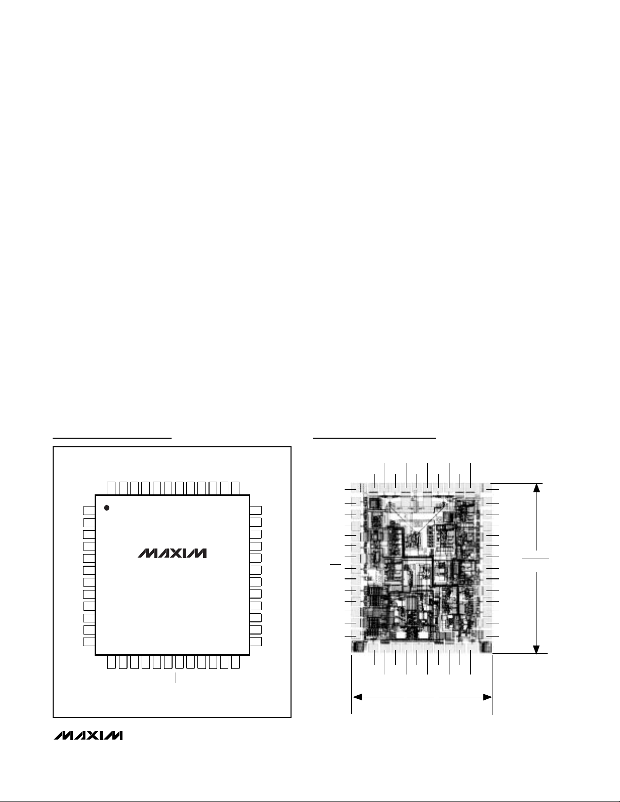
Pin Configuration Chip Topography
4243444546 383940
41
47
16
19
21
20
22
23
17 1814
15
2
3
4
5
6
7
8
9
10
11
26
27
28
29
30
31
32
33
34
35
VCC1
GND1
BIASMAX
MAX3867
TQFP
TOP VIEW
MODSET
GND2
APCSET
N.C.
GND2
N.C.
GND3
N.C.
CAPC37VCC3
ENABLE
SLWSTRT
GND1
FAIL
VCC1
N.C.
GND4
GND4
APCFILT
24
VCC4
MD
GND3
GND4
VCC4
N.C.
OUTOUT+
N.C.
VCC4
N.C.
25
BIAS
12
GND1
CLK-
CLK+
VCC1
GND1
VCC1
DATA-
DATA+
VCC1
GND1
1
36
GND3
GND2
48
13
VCC2
LATCH
LATCH
GND1
VCC1 CLK+ GND1 DATA- VCC1
CLK- VCC1 VCC1 DATA+ GND1
ENABLE
GND1
GND1
SLWSTRT
VCC1
FAIL
GND4
N.C.
APCFILT
GND4
VCC4
MDGND4N.C.OUT+VCC4
OUT-N.C. N.C. GND3VCCA
BIAS
VCC2
GND2
BIASMAX
MODSET
GND2
APCSET
N.C.
GND2
N.C.
GND3
N.C.
CAPC
VCC3
GND3
0.083"
(2.108mm)
0.070"
(1.778mm)

MAX3867
+3.3V, 2.5Gbps SDH/SONET Laser Driver
with Automatic Power Control
Maxim makes no warranty, representation or guarantee regarding the suitability of its products for any particular purpose, nor does Maxim assume any liability arising out of the application or use of any product or circuit and specifically disclaims any and all liability, including without limitation consequential or
incidental damages. “Typical” parameters can and do vary in different applications. All operating parameters, including “typicals” must be validated for
each customer application by customer’s technical experts. Maxim products are not designed, intended or authorized for use as components in systems
intended for surgical implant into the body, or other applications intended to support or sustain life, or for any other application in which the failure of the
Maxim product could create a situation where personal injury or death may occur.
12
____________________Maxim Integrated Products, 120 San Gabriel Drive, Sunnyvale, CA 94086 408-737-7600
© 1998 Maxim Integrated Products Printed USA is a registered trademark of Maxim Integrated Products.
Package Information
TQFPPO.EPS
 Loading...