For free samples & the latest literature: http://www.maxim-ic.com, or phone 1-800-998-8800.
For small orders, phone 1-800-835-8769.
General Description
The MAX3866 combined transimpedance preamplifier
and limiting postamplifier is intended for application in
SDH/SONET systems operating at 2.488Gbps. It operates from a single +3.3V or +5V supply and provides a
differential output signal. The differential outputs are
each 50Ω reverse terminated (100Ω differential termination) for low-noise and high-speed signal performance.
The small-signal bandwidth and noise performance is
specified for a source capacitance of 0.5pF. When the
MAX3866 is used with the PIN photodetector, sensitivities better than -22dBm can be achieved. The
MAX3866 is equipped with a programmable TTL lossof-power (LOP) output.
Applications
SDH/SONET Transmission Systems
PIN/Preamplifier Receivers
2.488Gbps ATM Receivers
Regenerators for SDH/SONET
Features
♦ Input Sensitivities Better than -22dBm (7.8µAp-p)
♦ Overdrive Capability Better than +1.4dBm
(2.5mAp-p)
♦ Single +3.3V or +5V Supply
♦ 165mW Power Dissipation (at 3.3V)
♦ 1.8GHz Analog Input Bandwidth
♦ Programmable Loss-of-Power Indicator
♦ 100Ω Differential Output
MAX3866
2.5Gbps, +3.3V Combined
Transimpedance/Limiting Amplifier
________________________________________________________________
Maxim Integrated Products
1
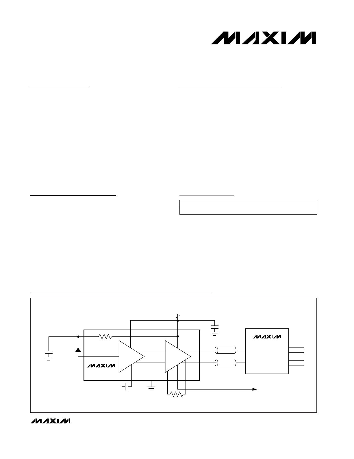
Zo = 50Ω
Zo = 50Ω
+3.3V
PHOTODIODE
CHF+ PDCCHF- INV
C
HF
R
PD
FIL
IN+
MAX3866
LIMITING
POSTAMP
PREAMP
LOP
OUT+
VCCS
VCCD
OUT-
CLOCK AND DATA
RECOVERY
MAX3875
200Ω
Typical Application Circuit
19-1433; Rev 1; 3/99
PART
MAX3866E/D (see Note)
TEMP. RANGE PIN-PACKAGE
Dice
Note: Dice are designed to operate over a -40°C to +120°C
junction temperature (T
j
) range, but are tested and guaranteed
at TA= +25°C.
Pad Configuration appears at end of data sheet.
Ordering Information

MAX3866
2.5Gbps, +3.3V Combined
Transimpedance/Limiting Amplifier
2 _______________________________________________________________________________________
ABSOLUTE MAXIMUM RATINGS
DC ELECTRICAL CHARACTERISTICS
(VCCD = VCCS = +3.3V ±5% or VCCD = +5.0V ±10%, VCCS = open, Tj= -40°C to +120°C, unless otherwise noted. Typical values
are at +3.3V and T
j
= +25°C.)
Stresses beyond those listed under “Absolute Maximum Ratings” may cause permanent damage to the device. These are stress ratings only, and functional
operation of the device at these or any other conditions beyond those indicated in the operational sections of the specifications is not implied. Exposure to
absolute maximum rating conditions for extended periods may affect device reliability.
Note 1: CIN= total capacitance on IN.
Note 2: AC parameters are guaranteed by design and characterization.
Note 3: See
Typical Operating Characteristics
for worst-case distribution.
Note 4: Hysteresis = 20 log (V
DEASSERT
/ V
ASSERT
).
Note 5: I
IN
= 2.5mA.
Note 6: PWD = [(2 · Pulse Width) - Period] / 2.
Note 7: External load not required for normal operation.
VCCD Voltage .......................................................-0.5V to +7.0V
VCCS Voltage...............0 ≤ VCCS ≤ VCCD and if VCCD ≥ 3.13V
then 3.13V ≤ VCCS ≤ VCCD
CHF+, CHF-, FIL, INV, LOP Voltage.......-0.5V to (VCCD + 0.5V)
IN-, IN+ Voltage.....................................................-0.5V to +1.0V
CPD+, CPD- Voltage................(VCCD - 1.6V) to (VCCD + 0.5V)
OUT+, OUT- Voltage................(VCCD - 1.1V) to (VCCD + 0.5V)
IN Current.......................................................................0 to 3mA
PDC Current..................................................................-1mA to 0
Operating Junction Temperature Range (T
j
).....-55°C to +125°C
Storage Temperature Range.............................-60°C to +160°C
Processing Temperature (Die).........................................+400°C
Load = 4.7kΩ to V
CCD
(Note 7)
Load = 4.7kΩ to V
CCD
(Note 7)
RL= 100Ω (differential), IIN≥ 7µAp-p
RL= 100Ω (differential)
CONDITIONS
Ω90 105 120Z
OUT
Differential Output Impedance
V0.84 0.95V
IN
mA50 73I
VCC
Supply Current
Input Bias Voltage
VV
CCD
- 0.1 V
CCD
V
OH
LOP Output High Voltage
V0.4V
OL
LOP Output Low Voltage
mVp-p100 145V
OD
Differential Output Voltage Swing
VV
CCD
- 0.12V
CM
Output Common-Mode Voltage
UNITSMIN TYP MAXSYMBOLPARAMETER
(Notes 5, 6)
20% to 80% (Note 5)
RPD= 510Ω
RPD= 510Ω
CIN= 0.5pF, Tj= +120°C
2.5Gbps, 223- 1 PRBS, BER ≤ 10
-10
,
CIN= 0.5pF, Tj= +120°C
Electrical (Note 4), low LOP assert,
RPD= 510Ω
f ≤ 2MHz, 100mVp-p
CONDITIONS
ps21 80PWDPulse-Width Distortion
ps50 70tr, t
f
Output Edge Speed
µA8.0LOP Deassert Level
µA0.9LOP Assert Level
dB3LOP Hysteresis
dB25 30PSRRPower-Supply Rejection Ratio
kHz100f
L
Low-Frequency Cutoff
nA433 566N
IN
Input-Referred RMS Noise
µAp-p7.8 (Note 3)I
IN
Input Sensitivity
GHz1.8BWSmall-Signal Bandwidth
UNITSMIN TYP MAXSYMBOLPARAMETER
AC ELECTRICAL CHARACTERISTICS
(VCCD = VCCS = +3.3V ±5% or VCCD = +5.0V ±10%, VCCS = open, Tj= -40°C to +120°C, unless otherwise noted. Typical values
are at +3.3V and T
j
= +25°C.) (Notes 1, 2)

MAX3866
2.5Gbps, +3.3V Combined
Transimpedance/Limiting Amplifier
_______________________________________________________________________________________
3
90
0
10 100
LOP ASSERT/DEASSERT
vs. R
PD
50
40
30
20
10
MAX3866 TOC01
RPD (Ω)
ASSERT/DEASSERT (µA)
60
70
80
ASSERT
DEASSERT
0
4
2
8
6
10
12
14
16
-60 -20 0-40 20 40 60 80 100
PULSE-WIDTH DISTORTION
vs. TEMPERATURE
MAX3866 TOC02
TEMPERATURE (¡C)
PWD (ps)
IN+ = 100µA
3.00
3.35
3.30
3.25
3.20
3.15
3.10
3.05
3.45
3.40
3.50
-50 -20 0-30 20 40 60 80 100
OUTPUT COMMON-MODE VOLTAGE
vs. TEMPERATURE
MAX3866 toc03
TEMPERATURE (°C)
COMMON-MODE VOLTAGE (V)
OUT+
OUT-
100
105
115
110
125
120
130
135
145
140
150
-60 -40 -20 0 20 40 60 80 100
DIFFERENTIAL OUTPUT VOLTAGE
vs. TEMPERATURE
MAX3866 TOC04
TEMPERATURE (°C)
DIFFERENTIAL OUTPUT VOLTAGE (mVp-p)
1k 10k
-20
-15
-10
-5
0
10
5
15
20
1 10 100
PULSE-WIDTH DISTORTION
vs. INPUT CURRENT
MAX3866 TOC07
INPUT CURRENT (µA)
PWD (ps)
30
40
60
50
70
80
90
100
-50 -10 10-30 30 50 70 90
SUPPLY CURRENT
vs. TEMPERATURE
MAX3866 TOC05
TEMPERATURE (°C)
SUPPLY CURRENT (mA)
3.14V
3.47V
1k 10k
100
105
110
115
120
130
125
135
140
1 10 100
OUTPUT VOLTAGE vs. INPUT CURRENT
MAX3866 TOC06
INPUT CURRENT (µA)
OUTPUT VOLTAGE (mVp-p)
ELECTRICAL EYE DIAGRAM
MAX3866 TOC08
50ps
INPUT = 8µAp-p, 2.5Gbps,
2
23
-1PRBS
R
L
= 100Ω DIFFERENTIAL
20mV/
div
ELECTRICAL EYE DIAGRAM
MAX3866 TOC09
50ps
20mV/
div
INPUT = 2.5mAp-p, 2.5Gbps,
2
23
-1PRBS
R
L
= 100Ω DIFFERENTIAL
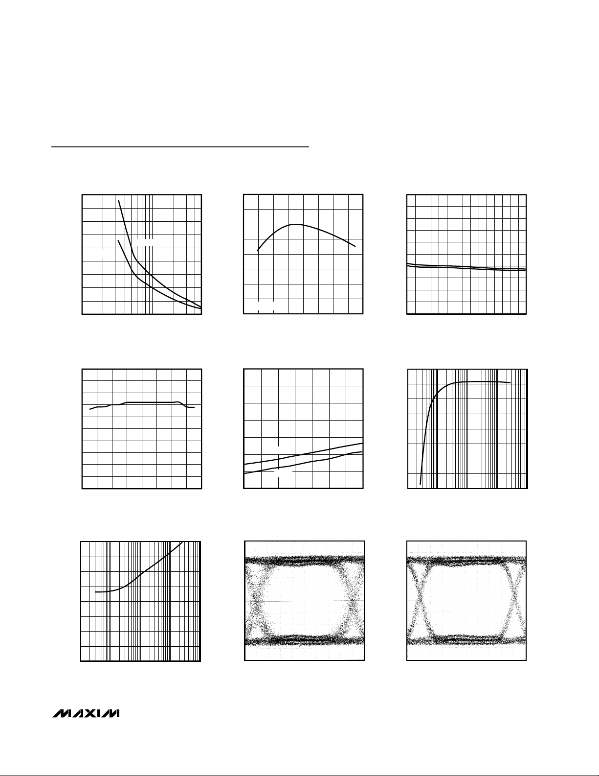
Typical Operating Characteristics
(V
CCD
= V
CCS
= +3.3V, TA = +25°C, unless otherwise noted.)

MAX3866
2.5Gbps, +3.3V Combined
Transimpedance/Limiting Amplifier
4 _______________________________________________________________________________________
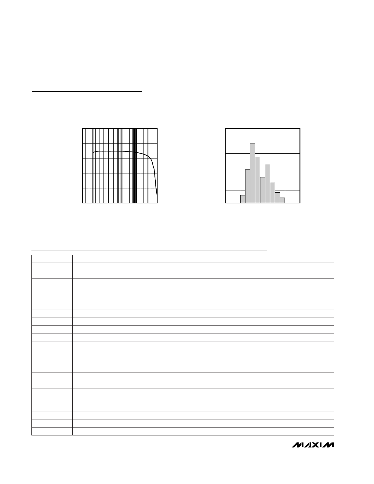
Typical Operating Characteristics (continued)
(V
CCD
= V
CCS
= +3.3V, TA = +25°C, unless otherwise noted.)
99
98
97
89
0.01 1 10
100
0.1
1000
SMALL-SIGNAL IMPEDANCE
vs. FREQUENCY
91
90
MAX3866 toc10
FREQUENCY (MHz)
TRANSIMPEDANCE
(20log (V
OUT
p-p/IN+))
93
96
95
94
92
0
10
5
20
15
25
30
7.717.28 8.14 8.57
DISTRIBUTION OF ELECTRICAL
SENSITIVITY (WORST CASE)
MAX3866 toc11
ELECTRICAL SENSITIVITY (µAp-p)
PERCENT OF UNITS (%)
VCC = +3.14V TO +5.5V
T
j
= +120°C
FUNCTION
VCCS
Positive Supply Voltage of Input Stage. Apply +3.3V if VCCD = +3.3V. If VCCD > +3.47V, disconnect from supply and decouple to GND.
CHF+
External Filter Capacitor. A capacitor connected between CHF+ and CHF- is used for setting the low-frequency
cutoff.
PAD NAME
CHF-
External Filter Capacitor. A capacitor connected between CHF+ and CHF- is used for setting the low-frequency
cutoff.
FIL On-Chip Resistor for Filtering Photodiode Supply Voltage (connected to VCCD on chip)
PDC
The voltage at this node programs the gain of the power detector. Connect a resistor between PDC and INV to
adjust the LOP threshold.
IN- No Connect
IN+ Signal Input
GND Electrical Ground
OUT+ Noninverted Data-Signal Output
OUT- Inverted Data-Signal Output
CPD+
Filter Node for Power Detector. A capacitor connected between CPD+ and CPD- will provide additional filtering
to the rectifier output within the power detector.
CPD-
Filter Node for Power Detector. A capacitor connected between CPD+ and CPD- will provide additional filtering
to the rectifier output within the power detector.
INV
Used for programming the gain of the power detector. Connect a resistor between PDC and INV to adjust the
LOP threshold.
Pad Description
VCCD Power-Supply Voltage
LOP TTL Output, Loss-of-Power, active high
 Loading...