

Page 1
General Description
The MAX3845 is a TMDS®2-to-4 fanout switch and
cable driver for multimonitor distribution of DVI™ or
HDMI™ signaling up to 1.65Gbps. Both inputs and outputs are standard TMDS signaling as per DVI and HDMI
standards. Because TMDS links are “point-to-point,”
buffering is required for fanout applications.
Four DVI/HDMI TMDS outputs are provided for fanout
distribution. Each TMDS output can be independently
sourced from either input or can be turned off. Each
TMDS input or output is composed of four differential
channels that can be arbitrarily assigned to the three
data signals and the 1/10th-rate clock. The data rate
depends on resolution, but it can vary from 250Mbps
(VGA) to 1.65Gbps (UXGA or 1080p/60).
Typical applications include multiroom display of the
same video source or industrial/commercial signage
applications such as airport monitors or trading room
floor displays. The MAX3845 includes selectable output
preemphasis that extends output cable reach up to an
additional 7m.
For DDC switching, use the companion MAX4814E 2:4
low-resistance CMOS crosspoint switch. DDC switching
is not required for applications that connect DDC to one
reference monitor only.
The MAX3845 can be configured to create a 2 x 8 or
4 x 4 switch (see the
Typical Operating Circuit
diagrams).
The MAX3845 is available in a 14mm × 14mm, 100-pin
TQFP-EP package and operates over the -10°C to
+85°C temperature range.
Applications
Digital Signage and Industrial Display
PC Monitor Distribution
Home A/V Receivers
DVI/HDMI Distribution Amplifiers
DVI/HDMI Crosspoint Switches
Features
o Two DVI/HDMI TMDS-Compatible Inputs and Four
DVI/HDMI TMDS-Compatible Outputs
o Save Power by Turning Off Unused Outputs
o Each Output Independently Selects Input 1 or
Input 2
o Three Preemphasis Settings Extend Cable Reach
Up to 7m
o Operation Up to 1.65Gbps
o 14mm x 14mm, 100-Pin TQFP Package with
Exposed Paddle for Heat Sinking
o 3.3V Power Supply
o TMDS Data (x3) and Clock (x1) Can Be Arbitrarily
Assigned to the Four Identical Switched Paths (A,
B, C, and D)
MAX3845
DVI/HDMI 2:4 TMDS Fanout Switch and
Cable Driver
________________________________________________________________
Maxim Integrated Products
1
Ordering Information
19-0798; Rev 0; 4/07
For pricing, delivery, and ordering information, please contact Maxim Direct at 1-888-629-4642,
or visit Maxim’s website at www.maxim-ic.com.
+
Denotes a lead-free package.
EP = Exposed pad.
Typical Operating Circuits continued at end of data sheet.
TMDS is a registered trademark of Silicon Image, Inc.
DVI is a trademark of Digital Display Working Group.
HDMI is a trademark of HDMI Licensing, LLC.
EVALUATION KIT
AVAILABLE
Pin Configuration appears at end of data sheet.
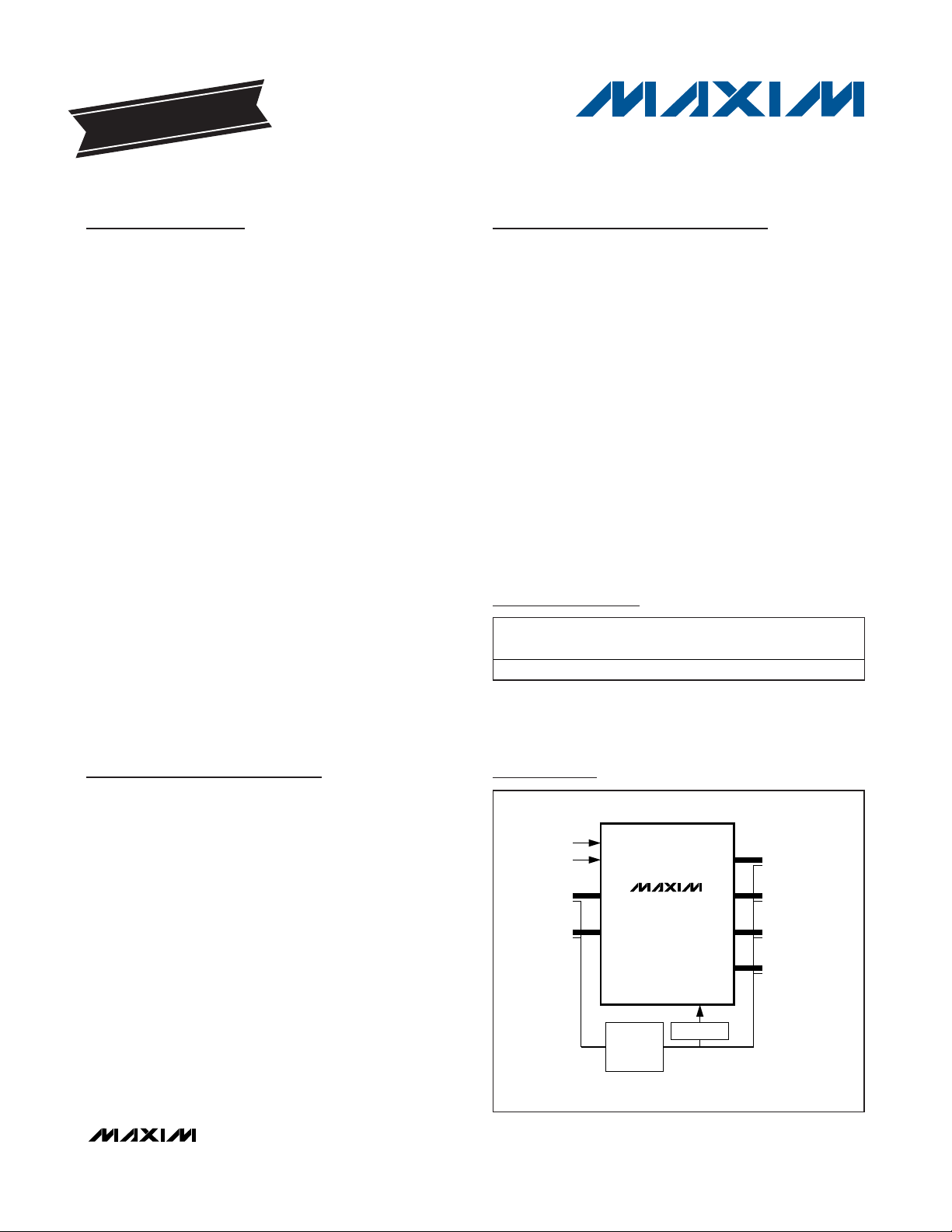
Typical Operating Circuit
PART TEMP RANGE PIN-PACKAGE
MAX3845UCQ+ -10°C to +85°C 100 TQFP-EP C100E-3
PKG
CODE
CONTROL
SIGNALS
VIDEO SOURCE 1
VIDEO SOURCE 2
2:4 FANOUT/SWITCH APPLICATION
IN_SEL[1:4]
PREEMPH[1:4]
MAX3845
2:4 DVI/HDMI TMDS
FANOUT SWITCH AND
CABLE DRIVER
2:4 CMOS
SWITCH x5
HOTPLUG[1:4]
BUFFER
DDC DATA, DDC CLK,
HOTPLUG, 5V, GND, (CEC)
OUTPUT TO DISPLAY 1
OUTPUT TO DISPLAY 2
OUTPUT TO DISPLAY 3
OUTPUT TO DISPLAY 4
Page 2
MAX3845
DVI/HDMI 2:4 TMDS Fanout Switch and
Cable Driver
2 _______________________________________________________________________________________
ABSOLUTE MAXIMUM RATINGS
ELECTRICAL CHARACTERISTICS
(VCC= 3.0V to +3.6V, TA= -10°C to +85°C. Typical values are at VCC= +3.3V, external terminations = 50Ω ±1%, TMDS rate =
250Mbps to 1.65Gbps, T
A
= +25°C, unless otherwise noted.) (Note 1)
Stresses beyond those listed under “Absolute Maximum Ratings” may cause permanent damage to the device. These are stress ratings only, and functional
operation of the device at these or any other conditions beyond those indicated in the operational sections of the specifications is not implied. Exposure to
absolute maximum rating conditions for extended periods may affect device reliability.
Supply Voltage Range (VCC) ................................-0.3V to +5.5V
Voltage Range at HOTPLUGx Pins ......................-0.3V to +6.0V
Voltage Range at LVTTL, LVCMOS, I/O Pins .......-0.3V to +5.5V
Voltage Range at CML Output Pins ......................-0.3V to +5.5V
Voltage Range at CML Input Pins
(CML short to GND duration < 1s)....................-0.3V to +4.0V
Voltage Between Any Input CML I/O
Complementary Pair ......................................................±3.3V
Voltage Range at LOSMUTE_EN ..........................-0.3V to +5.5V
Voltage Between Any Output CML I/O
Complementary Pair.......................................................±3.6V
Continuous Power Dissipation (TA= +70°C)
100-Pin TQFP-EP (derate 45.5mW/°C
above +70°C) ............................................................3636mW
Operating Junction Temperature .....................-55°C to +150°C
Storage Temperature Range ............................-55°C to +150°C
Die Attach Temperature ..................................................+400°C
Lead Temperature (soldering, 10s) .................................+300°C
PARAMETER SYMBOL CONDITIONS MIN TYP MAX UNITS
Power-Supply C urrent I
Supply-Noise Tolerance DC to 500kHz 50 mV
SKIN-EFFECT EQUALIZER PEAKING
Fixed Rx Equalizer
Compensation
Settable Tx Preemphasis
JITTER PERFORMANCE
Residual Deterministic Jitter
(Measured at end of cable
hav ing ideal skin-effect lo ss
and connectors, e.g., Gore Twin
Coax, Amphenol Skewclear
Twinax, with SMA connectors)
(Note 2)
Residua l Random Jitter (Note 3) Measured with source Tr/Tf = 250ps 1.5 2 ps
CML INPUTS (SOURCE SIDE)
Differentia l-Input Voltage Swing V
Common-Mode Input Voltage VCM VCC - 1000 V
Input Voltage When Disconnected VCC - 10 VCC + 10
PREEMPH[1:4] = h igh, OUT_LEVEL = high,
CC
current into V
Gain at 825MHz 1
PREEMPHx pin = low 0
PREEMPHx pin = open 3
PREEMPHx pin = high 6
200 back
termination
No back
termination
At cable input 400 2000 mV
ID
pins, 1200mV
CC
0dB cable loss, no
preemphasis
3dB cable loss, +3dB
preemphasis
6dB cable loss, +6dB
preemphasis
0dB cable loss, no
preemphasis
3dB cable loss, +3dB
preemphasis
6dB cable loss, +6dB
preemphasis
P-P
= V
IN
454 626 mA
0.04 0.12
0.05 0.12
0.07 0.12
0.07 0.2
0.08 0.2
0.10 0.2
CC
P-P
dB
UI
RMS
P-P
mV
Page 3
MAX3845
DVI/HDMI 2:4 TMDS Fanout Switch and
Cable Driver
_______________________________________________________________________________________ 3
Note 1: AC specifications are guaranteed by design and characterization.
Note 2: Test pattern is a 2
10
- 1 PRBS + 20 ones + 210- 1 PRBS (inverted) + 20 zeros.
Note 3: Test pattern is a 1111 0000 pattern at 1.65Gbps.
ELECTRICAL CHARACTERISTICS (continued)
(VCC= 3.0V to +3.6V, TA= -10°C to +85°C. Typical values are at VCC= +3.3V, external terminations = 50Ω ±1%, TMDS rate =
250Mbps to 1.65Gbps, T
A
= +25°C, unless otherwise noted.) (Note 1)
PARAMETER SYMBOL CONDITIONS MIN TYP MAX UNITS
Input Resistance R
Input LOS/Mute Threshold Differential peak-peak 150 mV
Input LOS/Mute Response Time
Input Return Loss Differential, 1.6GHz 19 dB
CML OUTPUTS (CABLE SIDE)
Differentia l-Output Voltage Swing V
Output-Voltage High VOH Single-ended, no back termination VCC - 10 VCC + 10
Output Voltage During PowerDown
Rise/Fall Time 20% to 80% (TA = 0°C to +85°C) 75 90 140
Intrapair Skew 12 40
Interpair Skew
CONTROL INTERFACE
LVTTL Input High Voltage V
LVTTL Input Low Voltage V
LVTTL Input High Current V
LVTTL Input Low Current V
HOTPLUGx Input High Voltage Typical input 30k to GND VCC - 0.2 5.5
HOTPLUGx Input Low Voltage 1.5
Single-ended 45 50 55
IN
Deas sert mute 1.2
Assert mute 0.6
No preemphasis, no back termination,
OUT_LEVEL = low
OD
No preemphasis, 200 back termination,
OUT_LEVEL = h igh
V
Single-ended, PWRDWN_x = low or
OFF
IH
IL
= 0V
V
CC
Worst case among A, B, C, and D of an
output
2.0
All except IN_SELx pins 1.0
IN_SELx pins 0.8
< VIN < V
IH(MIN)
< VIN < V
IL(MIN)
IH(MAX)
IL(MAX)
900 1050 1200
825 925 1050
V
- 10 VCC + 10
CC
35 60
100
All except
OUT_LEVEL pin
OUT_LEVEL pin 500
150
μs
mV
mV
ps
V
μA
V
P-P
Page 4
MAX3845
DVI/HDMI 2:4 TMDS Fanout Switch and
Cable Driver
4 _______________________________________________________________________________________
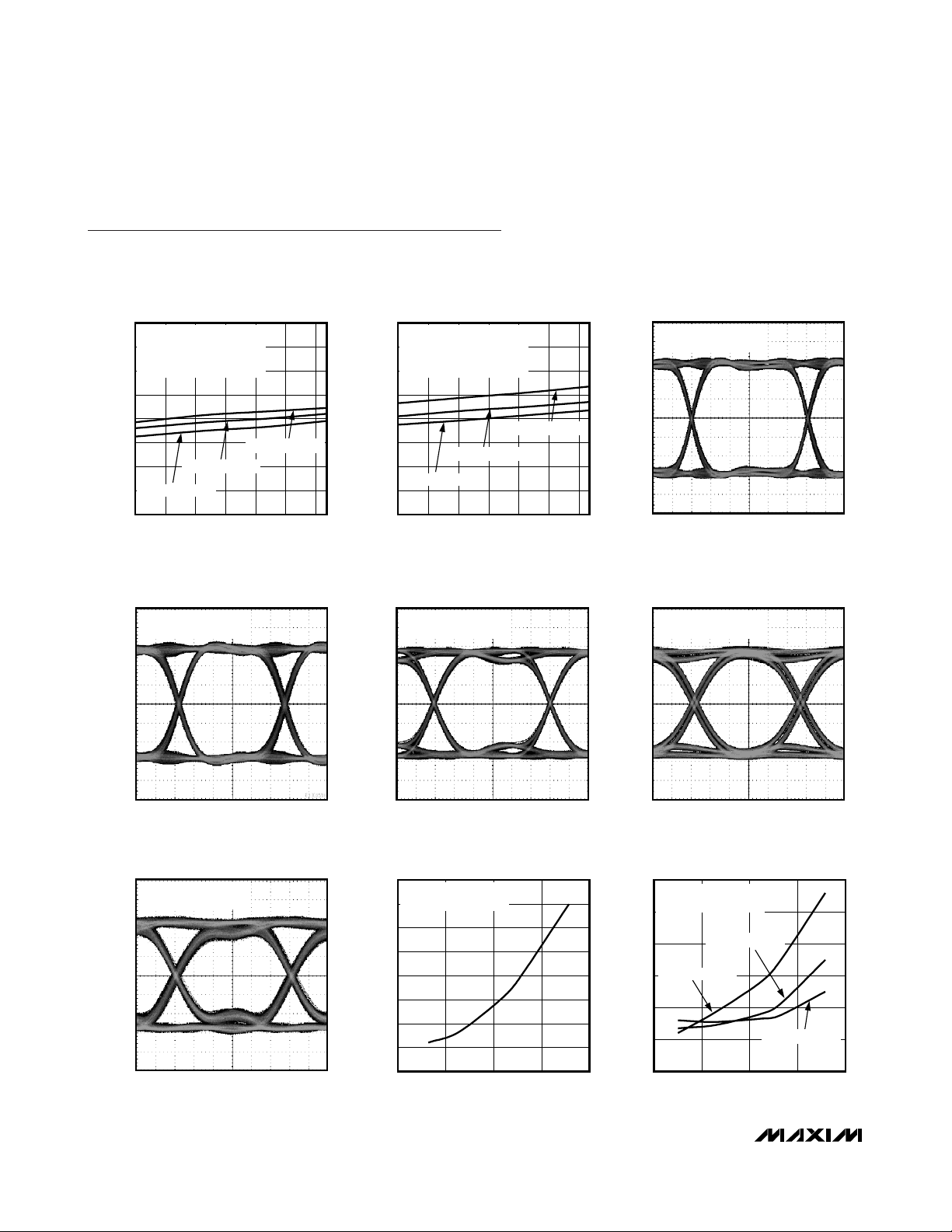
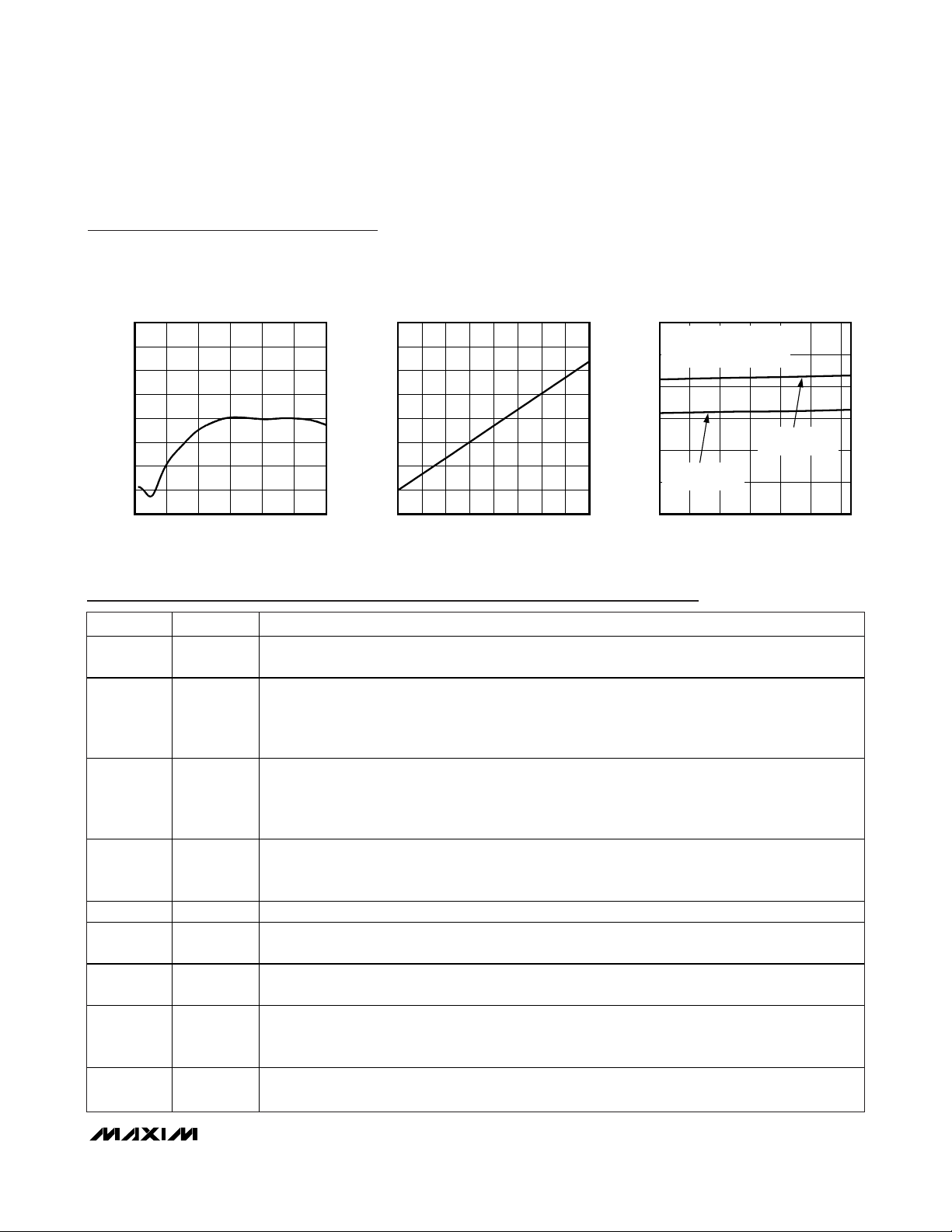
Typical Operating Characteristics
(Typical values are at VCC= +3.3V, TA= +25°C, data pattern = 210- 1 PRBS + 20 ones + 210- 1 PRBS (inverted) + 20 zeros, unless
otherwise noted.)
SUPPLY CURRENT
vs. AMBIENT TEMPERATURE
MAX3845 toc01
AMBIENT TEMPERATURE (°C)
I
CC
(mA)
80655 20 35 50
360
380
400
420
440
460
480
500
340
-10
OUT_LEVEL = LOW,
ALL INPUTS/OUTPUTS ACTIVE,
PREEMPHASIS SAME ON ALL
OUTPUT CHANNELS
0dB PREEMPHASIS
3dB PREEMPHASIS
6dB PREEMPHASIS
SUPPLY CURRENT
vs. AMBIENT TEMPERATURE
MAX3845 toc02
AMBIENT TEMPERATURE (°C)
I
CC
(mA)
80655 20 35 50
360
380
400
420
440
460
480
500
340
-10
OUT_LEVEL = HIGH,
ALL INPUTS/OUTPUTS ACTIVE,
PREEMPHASIS SAME ON ALL
OUTPUT CHANNELS
0dB PREEMPHASIS
3dB PREEMPHASIS
6dB PREEMPHASIS
OUTPUT EYE DIAGRAM AT 1.65Gbps
SHORT LOW-LOSS SMA CABLE
MAX3845 toc03
100ps/div
150mV/div
0dB PREEMPHASIS
200Ω BACK TERMINATION
OUTPUT EYE DIAGRAM AT 2.25Gbps
SHORT LOW-LOSS SMA CABLE
MAX3845 toc04
80ps/div
150mV/div
0dB PREEMPHASIS
200Ω BACK TERMINATION
OUTPUT EYE DIAGRAM AT 1.65Gbps
6dB LOSS, 24AWG, 25ft TWIN-AX CABLE
MAX3845 toc05
100ps/div
150mV/div
6dB PREEMPHASIS
200Ω BACK TERMINATION
OUTPUT EYE DIAGRAM AT 2.25Gbps
6dB LOSS, 24AWG, 25ft TWIN-AX CABLE
MAX3845 toc06
80ps/div
150mV/div
6dB PREEMPHASIS
200Ω BACK TERMINATION
OUTPUT EYE DIAGRAM AT 1.65Gbps
THROUGH 2m DVI TO HDMI CABLE
MAX3845 toc07
100ps/div
150mV/div
6dB PREEMPHASIS
200Ω BACK TERMINATION
JITTER vs. INPUT-SIDE CABLE LOSS
AT 825 MHz
MAX3845 toc08
CABLE LOSS (dB)
JITTER (ps
P-P
)
642
20
40
60
80
100
120
140
160
0
08
DATA RATE = 1.65Gbps
200Ω BACK TERMINATION
JITTER vs. OUTPUT-SIDE CABLE LOSS
AT 825 MHz
MAX3845 toc09
CABLE LOSS (dB)
JITTER (ps
P-P
)
642
20
40
60
80
100
120
0
08
0dB PREEMPHASIS
3dB PREEMPHASIS
6dB PREEMPHASIS
DATA RATE = 1.65Gbps
200Ω BACK TERMINATION
Page 5
MAX3845
DVI/HDMI 2:4 TMDS Fanout Switch and
Cable Driver
_______________________________________________________________________________________
5
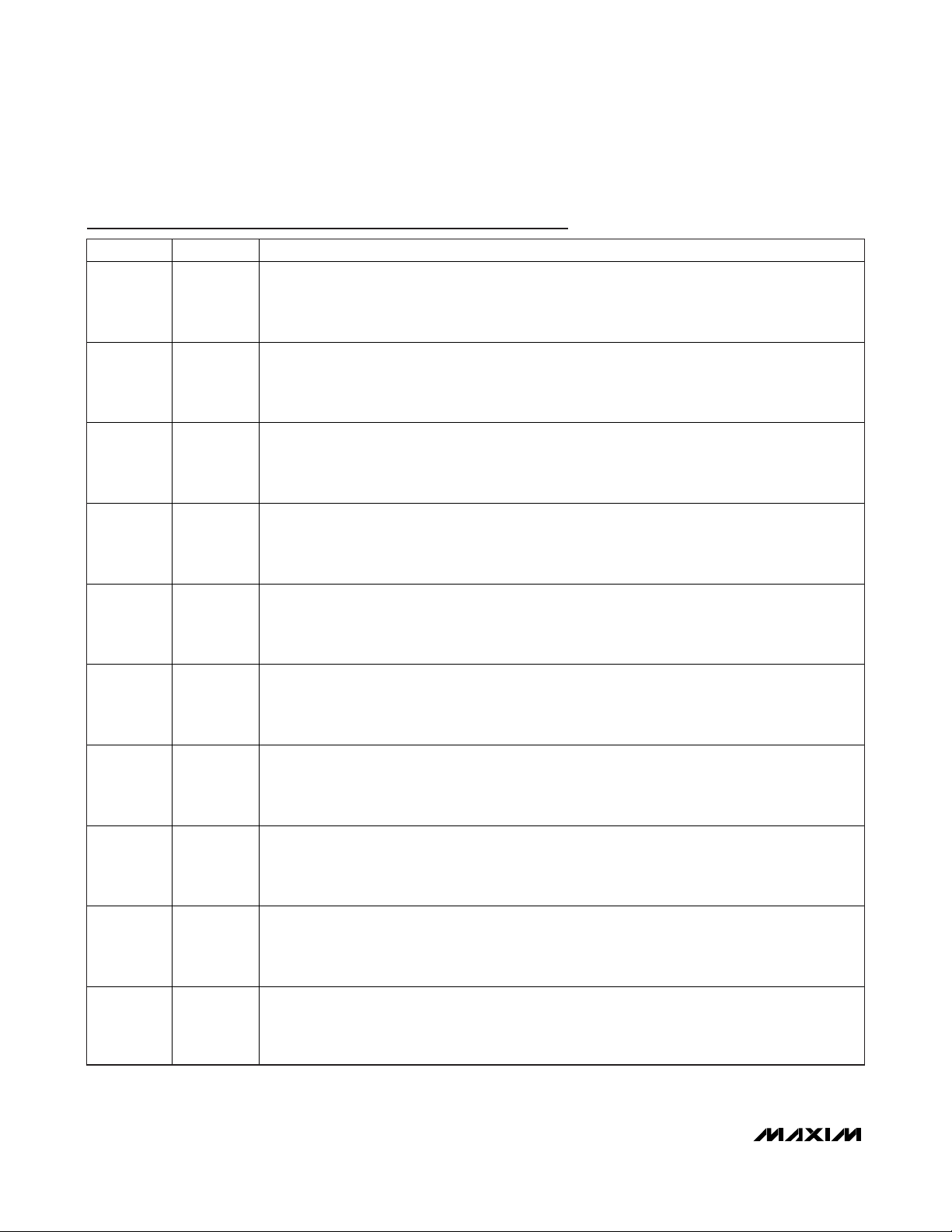
Typical Operating Characteristics (continued)
(Typical values are at VCC= +3.3V, TA= +25°C, data pattern = 210- 1 PRBS + 20 ones + 210- 1 PRBS (inverted) + 20 zeros, unless
otherwise noted.)
Pin Description
DIFFERENTIAL-INPUT RETURN LOSS
vs. FREQUENCY
0
-5
-10
-15
-20
GAIN (dB)
-25
-30
-35
-40
0 3000
FREQUENCY (MHz)
1.6
1.5
MAX3845 toc10
1.4
1.3
1.2
TEMP (V)
1.1
1.0
0.9
0.8
25002000500 1000 1500
-10 150
TEMP VOLTAGE
vs. JUNCTION TEMPERATURE
JUNCTION TEMPERATURE (°C)
PIN NAME FUNCTION
1, 4, 7, 10,
97, 100
Positive Power-Supply Connection. Powers input channel 1 and output channels 1 and 2.
V
CC1
3000
2500
MAX3845 toc11
2000
1500
1000
POWER DISSIPATION (mW)
500
0
13011010 30 50 70 90
-10
POWER DISSIPATION
vs. AMBIENT TEMPERATURE
ALL INPUTS/OUTPUTS ACTIVE,
PREEMPHASIS SAME ON ALL
OUTPUT CHANNELS
6dB PREEMPHASIS
OUT_LEVEL = HIGH
0dB PREEMPHASIS
OUT_LEVEL = LOW
AMBIENT TEMPERATURE (°C)
80655035205
MAX3845 toc12
IN1_B+,
2, 5, 8, 98
IN1_C+,
IN1_D+,
IN1_A+
IN1_B-,
3, 6, 9, 99
IN1_C-,
IN1_D-,
IN1_A-
11 PWRDWN_1
12 V
Positive Power-Supply Connection. Powers the temp-sense circuitry.
CC3
13 LOSMUTE_EN
14 TEMP
15 PWRDWN_2
16, 19, 22,
25, 26, 29
V
Positive Power-Supply Connection. Powers input channel 2 and output channels 3 and 4.
CC2
Noninverting TMDS CML Input, Channel 1
Inverting TMDS CML Input, Channel 1
Power-Down, LVTTL/LVCMOS Input. Force high or leave open to power down input channel 1. Force
low to enable input channel 1. The MAX3845 powers down if both PWRDWN_1 and PWRDWN_2 are
forced high or left open.
LOS MUTE Enable Input. Connect to V
for typical operation. Connect to GND to disable the LOS
CC
MUTE function.
Junction Temperature Sensor. Attach a ground-referenced vo ltage DMM to this pin to measure the
die’s junction temperature (see the V
pin description). Leave open if not used.
CC3
Power-Down, LVTTL/LVCMOS Input. Force high or leave open to power down input channel 2. Force
low to enable input channel 2. The MAX3845 powers down if both PWRDWN_1 and PWRDWN_2 are
forced high or left open.
Page 6
MAX3845
DVI/HDMI 2:4 TMDS Fanout Switch and
Cable Driver
6 _______________________________________________________________________________________
Pin Description (continued)
PIN NAME FUNCTION
IN2_A+,
17, 20, 23,
27
18, 21, 24,
28
30, 61, 65,
96
31, 62, 64,
95
IN2_B+,
IN2_C+,
IN2_D+
IN2_A-,
IN2_B-,
IN2_C-,
IN2_D-
IN_SEL4,
IN_SEL3,
IN_SEL2,
IN_SEL1
PREEMPH4,
PREEMPH3,
PREEMPH2,
PREEMPH1
Noninverting TMDS, CML Input, Channel 2
Inverting TMDS, CML Input, Channel 2
Input Select, LVTTL Input. Force high to select input channel 1. Force low to select input channel 2.
Leave open to di sable the output channel.
Preemphasis Select, LVTTL/LVCMOS Input. Force h igh for 6dB of output preemphasis. Leave open
for 3dB of output preemphas is. Force low for 0dB of output preemphasis (normal).
32, 46, 80,
94
33, 36, 39,
42, 45, 47,
50, 51, 54,
57, 60
34, 37, 40,
43
35, 38, 41,
44
48, 52, 55,
58
49, 53, 56,
59
HOTPLUG4,
HOTPLUG3,
HOTPLUG2,
HOTPLUG1
GND2 Supply Ground. Ground connection for input channel 2 and output channels 3 and 4.
OUT4_D-,
OUT4_C-,
OUT4_B-,
OUT4_A-
OUT4_D+,
OUT4_C+,
OUT4_B+,
OUT4_A+
OUT3_D-,
OUT3_C-,
OUT3_B-,
OUT3_A-,
OUT3_D+,
OUT3_C+,
OUT3_B+,
OUT3_A+,
Hotplug Sense Input. Connect this pin to the di spla y’s HOTPLUGx signal (buffered) to allow
automatic power-down of the associated output when the display is disconnected. A low-cost quad
5V, noninverting CMOS gate (74ACT32 series) is recommended to buffer the MAX3845 from the
HOTPLUGx pin to match HOTPLUG level specifications. If this feature is not used, connect to V
Inverting TMDS, CML Output, Channel 4
Noninverting TMDS, CML Output, Channel 4
Inverting TMDS, CML Output, Channel 3
Noninverting TMDS, CML Output, Channel 3
CC
.
Page 7

MAX3845
DVI/HDMI 2:4 TMDS Fanout Switch and
Cable Driver
_______________________________________________________________________________________ 7
Pin Description (continued)
PIN NAME FUNCTION
Output Level Select, LVTTL/LVCMOS Input. Force pin low when no back termination i s u sed (11mA
63 OUT_LEVEL
66, 69, 72,
75, 76, 79,
81, 84, 87,
90, 93
67, 70, 73,
77
68, 71, 74,
78
82, 85, 88,
91
GND1 Supply Ground. Ground connection for input channel 1 and output channels 1 and 2.
OUT2_D-,
OUT2_C-,
OUT2_B-,
OUT2_A-
OUT2_D+,
OUT2_C+,
OUT2_B+,
OUT2_A+
OUT1_D-,
OUT1_C-,
OUT1_B-,
OUT1_A-
of tai l current). Force pin high when 200 back termination resistors are used (14mA of tail
current).
Inverting TMDS, CML Output, Channel 2
Noninverting TMDS, CML Output, Channel 2
Inverting TMDS, CML Output, Channel 1
OUT1_D+,
83, 86, 89,
92
— EP
OUT1_C+,
OUT1_B+,
OUT1_A+
Noninverting TMDS, CML Output, Channel 1
Ground. The exposed pad must be soldered to the circuit board ground for proper thermal and
electrical operation.
Page 8

MAX3845
DVI/HDMI 2:4 TMDS Fanout Switch and
Cable Driver
8 _______________________________________________________________________________________
Detailed Description
The MAX3845 2:4 DVI/HDMI fanout switch and cable
driver accept differential CML input data at rates of
250Mbps up to 1.65Gbps (individual channel data
rate). The input portion of the device consists of two
independent TMDS inputs, each having four fixed-level
equalizers, four limiting amplifiers, a loss-of-signal
(LOS) detector, and power-down control. The output
portion of the device consists of four independent
TMDS outputs, each having four multiplexers, four output buffers with selectable preemphasis, HOTPLUG
detection, and channel selection control (Figure 1).
Fixed Input Equalization
All four differential pairs on the MAX3845’s TMDS
inputs have fixed-level equalizers to compensate for 0in
to 6in of FR4 PCB losses. The signal boost is approximately 1dB at 825MHz. If more equalization is desired,
use the MAX3814 or MAX3815 in front of the MAX3845
to accommodate long cable lengths.
Limiting Amplifiers
Limiting amplifiers follow the equalizer block to ensure
proper signal levels are achieved for the multiplexers.
Loss-of-Signal (LOS) Detectors
Input channel 1 has an LOS detector attached to the
IN1_B pair. For input channel 2 the LOS detector is
attached to the IN2_C pair. If the received-signal amplitude is smaller than 150mV
P-P
(typical) at IN1_B, all
output channels selected to input 1 are muted.
Likewise, if a signal smaller than 150mV
P-P
(typical) is
at IN2_C, all output channels selected to input 2 are
muted.
Multiplexers
Each MAX3845 output has four multiplexers, one for
each signal pair contained in the TMDS channel. These
connect the output to either input 1 or input 2. The
IN_SELx pins control the multiplexers.
Preemphasis Drivers
The preemphasis drivers have three selectable levels
of preemphasis: 0dB, 3dB, and 6dB. The preemphasis
drivers provide a precompensated signal that allows for
extended length cables to be used at the output.
Applications Information
MAX3845 in HDMI 1.3 Systems
The MAX3845 is designed and characterized to operate from 250Mbps to 1.65Gbps. HDMI 1.3 specifies up
to 2.25Gbps for 1080p “deep color” and allows a maximum data rate of 3.4Gbps on each of the three data
pairs. The MAX3845 operates normally in an HDMI 1.3
system up to 1.65Gbps. The MAX3845 operates at data
rates above 1.65Gbps with reduced jitter performance.
See the
Typical Operating Characteristics
section for
more information.
MAX3845 in HDCP Systems
High-bandwidth digital content protection (HDCP) is a
copy protection system employed in some DVI and
most HDMI interfaces. Video data is encrypted at the
transmitter and decrypted at the receiver. The data
scrambling is dependent upon shared keys established
during the authentication protocol that occurs over the
DDC channel (between the video source and the display). The MAX3845 does not decrypt or reencrypt
data. Therefore, HDCP-encrypted video routed through
the MAX3845 is only viewable on the display to which
the DDC channel is connected. For applications that
employ HDCP, the MAX3845 acts as a dual 1:4 switch
and not as a fanout device. This means that one video
source can be selected to drive any one of four displays, but the video source cannot be replicated on
more than one display at the time. Fanout is possible in
non-HDCP applications, allowing one video source to
simultaneously drive up to four displays.
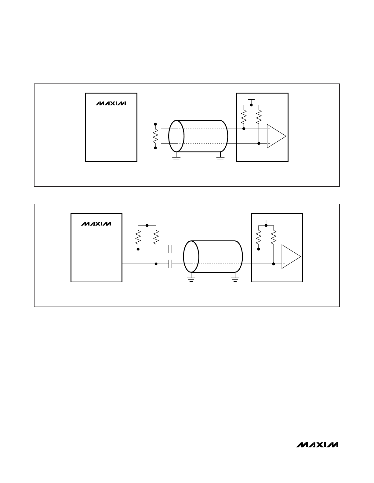
Output Level Control, Back Termination,
and AC-Coupling
The OUT_LEVEL pin is an LVTTL input that allows the
user to select between standard output drive current
(11mA) or increased output drive current (14mA). The
increased output current setting allows back termination resistors to be used on the outputs. The use of
back terminations is highly recommended for best signal integrity (see Figures 2 and 3).
If OUT_LEVEL is set low, the standard output drive current (11mA) is consistent with DVI/HDMI architecture
and common-mode levels. As per standard, no back
termination is used so no reflected energy can be
absorbed.
If OUT_LEVEL is set high, the output drive current is
increased to 14mA and allows the use of back termination resistors. Two options are available: a differential
back termination resistor or two single-ended pullup
resistors (see Figures 2 and 3).
Page 9

MAX3845
DVI/HDMI 2:4 TMDS Fanout Switch and
Cable Driver
_______________________________________________________________________________________ 9
Figure 1. Functional Diagram
OUT_LEVEL
EXAMPLE:
MAX3815
CLKLOS
EXAMPLE:
MAX3815
CLKLOS
IN1_[A-D]
PWRDWN_1
LOSMUTE_EN
IN2_[A-D]
PWRDWN_2
2:4 DVI FANOUT
SWITCH AND CABLE DRIVER
EQEQ LA
LOS 1
>MUTE
-
PD INPUT MACRO 1
EQEQ LA
LOS 2
>MUTE
-
PD INPUT MACRO 2
OUTPUT MACRO 1
OUTPUT MACRO 2
OUTPUT MACRO 3
OUTPUT MACRO 4
PE
PE
PE
OUT1_[A-D]
HOTPLUG1
PREEMPH1
IN_SEL1
OUT2_[A-D]
HOTPLUG2
PREEMPH2
IN_SEL2
OUT3_[A-D]
HOTPLUG3
PREEMPH3
IN_SEL3
DVI OR
HDMI
CONNECTOR
DVI OR
HDMI
CONNECTOR
DVI OR
HDMI
CONNECTOR
TEMP (DIE TEMP SENSE)
IN_SELx
DECODER
HIGH
OPEN
ANALOG TEMP
SENSE
POWER-DOWN LOGIC FOR EACH OF 4 OUTPUT MACROS
PWRDWN_ [OUTPUT MACRO x], WHERE x = 1, 2, 3, OR 4, IF:
[PWRDWN_1 = LOW] OR [LOS 1 = HIGH]
[PWRDWN_2 = HIGH] OR [LOS 2 = HIGH]
LOW
[HOTPLUGx = LOW OR OPEN]
AND
[IN_SELx = HIGH]
OR
AND
[IN_SELx = LOW]
OR
[IN_SELx = OPEN]
PE
R 2 x R
OUT4_[A-D]
HOTPLUG4
PREEMPH4
IN_SEL4
ON-CHIP SIGNAL:
POWER-DOWN
OUTPUT MACRO x
DVI OR
HDMI
CONNECTOR
Page 10
MAX3845
Back termination greatly reduces signal degradation
caused by reflections coming off DVI/HDMI connectors
and any other transmission line discontinuities. Much of
the reflected energy off a DVI connector, for example,
is absorbed by the back termination resistance rather
than reflected forward, causing eye closure. For the
cases shown in Figures 2 and 3, the return loss is
approximately 9.5dB. In other words, about 90% of the
reflected energy is absorbed by the back termination
resistors. Maxim strongly recommends using back termination to maximize the MAX3845’s performance.
The differential back termination options reduce the
common-mode output voltage seen by the TMDS
receiver to approximately VCC- 350mV (Table 1).
The single-ended back termination option allows for
AC-coupling between the MAX3845 and a TMDS
receiver, so long as the TMDS receiver is tolerant of an
input common-mode voltage equal to VCC(HDMI 1.2 or
later).
DVI/HDMI 2:4 TMDS Fanout Switch and
Cable Driver
10 ______________________________________________________________________________________
Figure 2. DC-Coupled Differential Back Termination
Figure 3. AC-Coupled Single-Ended Back Termination
+3.3V
MAX3845
TMDS
OUTPUT
PAIR
200Ω*
300Ω*
Z
= 100
OR
0(DIFF)
50Ω
TMDS
RECEIVER
*BACK TERMINATION RESISTOR IS LOCATED AS CLOSE AS POSSIBLE TO THE MAX3845.
50Ω
Rx
+3.3V
MAX3845
OUTPUT
*BACK TERMINATION RESISTORS ARE LOCATED AS CLOSE AS POSSIBLE TO THE MAX3845.
TMDS
PAIR
100Ω* 100Ω*
0.1μF
0.1μF
+3.3V
50Ω
50Ω
Z
0(DIFF)
= 100
Rx
TMDS
RECEIVER
Page 11
MAX3845
DVI/HDMI 2:4 TMDS Fanout Switch and
Cable Driver
______________________________________________________________________________________ 11
Temperature Sense
Pin 14, TEMP, allows the on-die temperature to be
sensed as an analog voltage output. To sense the die
temperature, measure the DC voltage at TEMP. The
approximate die temperature can be determined using
the following equation:
TJ = (V
TEMP
- 0.93) x 297
Also see the
Typical Operating Characteristics
section
for more information.
Power-Down
The power-down inputs (PWRDWN_1 and PWRDWN_2)
reduce power consumption by powering down the chosen input and all outputs that are selected to that input.
For example, when output channels 1 and 4 are selected to transmit input channel 2, and channel 2 is powered down, both outputs 1 and 4 are also powered
down.
Hotplug Detect
Each output channel has a HOTPLUGx detection pin
associated with it. This pin is designed to detect
whether a monitor’s hotplug connection is attached. If
HOTPLUGx is low (less than 1.5V), the associated output is powered down. If HOTPLUGx is higher than
VCC- 0.2V, up to 5.5V, the associated output is powered up.
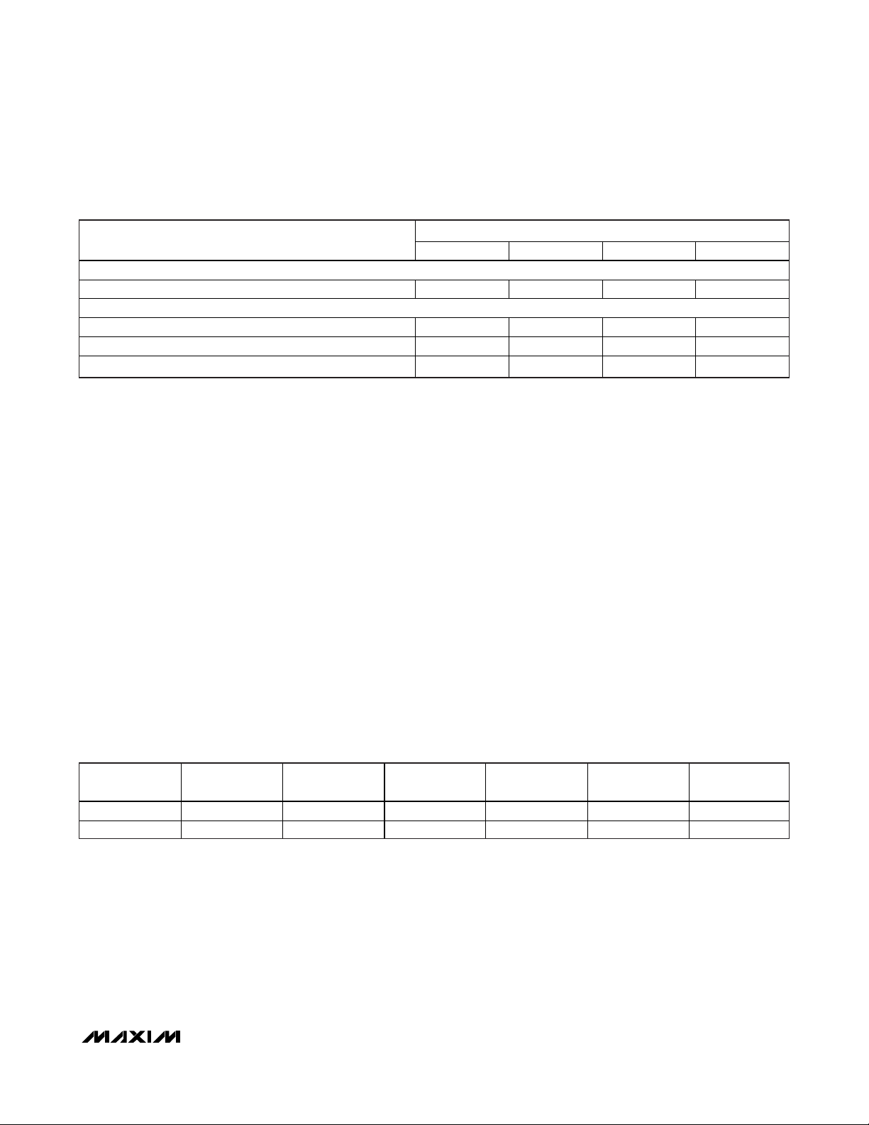
Activating an Output
Several things must occur for an output to be active.
Table 2 lists the required inputs to enable an output.
Cable Selection
Good quality cable is recommended for good performance. Deterministic jitter (DJ) can be caused by differential-to-common-mode conversion (or vice versa)
within a twisted pair (STP or UTP), usually a result of
cable twist or dielectric imbalance. Refer to Application
Note
HFAN-4.5.4: ‘Jitter Happens’ when a Twisted Pair
is Unbalanced
for more information.
Table 1. Output Levels With and Without Back Termination
Table 2. Output Enable Requirements
CONDITIONS
PREEMPHx = LOW, OUT_LEVEL = LOW (Output Drive Current = 11mA)
No back termination 1100mV
PREEMPHx = LOW, OUT_LEVEL = HIGH (Output Drive Current = 14mA)
Differentia l 200 back terminations (DC-coupled) 950mV
Differentia l 300 back terminations (DC-coupled) 1050mV
Single-ended, 2x 100 bac k terminat ion s (AC-coup led) 950mV
VOLTAGES AT THE INPUT OF THE TMDS RECEIVER (TYPICAL)
V
DIFF
VCC - 275mV VCC V
P-P
VCC - 350mV VCC - 120mV VCC - 585mV
P-P
VCC - 350mV VCC - 90mV VCC - 615mV
P-P
V
P-P
V
CM
V
CC
V
H
+ 240mV VCC - 240mV
CC
V
- 550mV
CC
L
OUTPUT x
STATE
INPUT 1 HIGH HIGH LOW Don’t care LOW Don’t care
INPUT 2 LOW HIGH Don’t care LOW Don’t care LOW
IN_SELx
CONDITION
HOTPLUGx
CONDITION
PWRDWN_1
CONDITION
PWRDWN_2
CONDITION
LOS 1
CONDITION
LOS 2
CONDITION
Page 12
MAX3845
Layout Considerations
The data inputs and outputs are the MAX3845’s most
critical paths, and great care should be taken to minimize discontinuities on these transmission lines
between the connector and the IC. Here are some suggestions for maximizing the performance of the
MAX3845:
• Maintain 100Ω differential transmission line impedance into and out of the MAX3845.
• The data and clock inputs should be wired directly
between the cable connector and IC without stubs.
• An uninterrupted ground plane should be positioned beneath the high-speed I/Os.
• Ground path vias should be placed close to the IC
and the input/output interfaces to allow a return current path to the IC and the DVI/HDMI cable.
• Use good high-frequency layout techniques and
multilayer boards with an uninterrupted ground
plane to minimize EMI and crosstalk.
For more information, refer to the schematic and board
layers of the Maxim evaluation kit,
MAX3845EVKIT
.
Exposed-Pad Package and Thermal
Considerations
The exposed pad on the 100-pin TQFP-EP provides a
very low thermal resistance path for heat removal from
the IC. The pad is also electrical ground on the
MAX3845 and must be soldered to the circuit board
ground for proper thermal and electrical performance.
Refer to Maxim Application Note
HFAN-08.1: Thermal
Considerations of QFN and Other Exposed-Paddle
Packages
for additional information.
Because the MAX3845 is a high-power device, it is
important to ensure that good heat dissipation is incorporated into the PCB design. The device’s temperaturesense pin (TEMP) allows estimation of the junction
temperature to be made while the MAX3845 is operating. This information can be used to determine if the
PCB layout is dissipating heat properly.
DVI/HDMI 2:4 TMDS Fanout Switch and
Cable Driver
12 ______________________________________________________________________________________
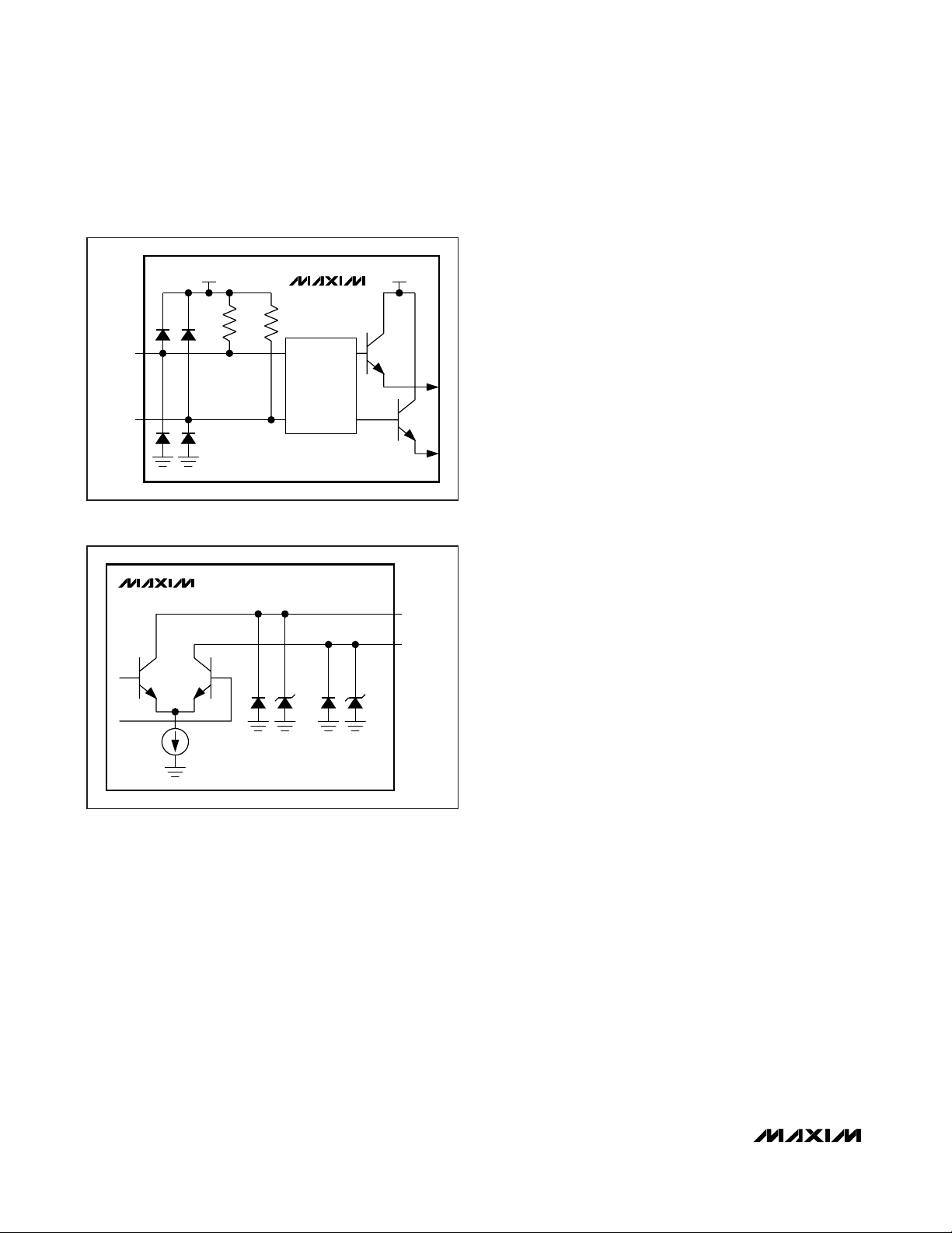
Interface Models
Figure 4. Simplified Input Circuit Schematic
Figure 5. Simplified Output Circuit Schematic
V
CC
50Ω
50Ω
TMDS
INPUT+
TMDS
INPUT-
MAX3845
*TVS IS A "TRANSIENT VOLTAGE
SUPPRESSOR" CLAMP-CIRCUIT.
V
CC
MAX3845
EQUALIZATION
NETWORK
TMDS
OUTPUT+
TMDS
OUTPUT-
TVS* TVS*
Page 13

MAX3845
DVI/HDMI 2:4 TMDS Fanout Switch and
Cable Driver
______________________________________________________________________________________ 13
Pin Configuration
TOP VIEW
LOSMUTE_EN
V
CC1
INT1_B+
INT1_B-
V
CC1
IN1_C+
IN1_C-
V
CC1
IN1_D+
IN1_D-
V
CC1
PWRDWN_1
V
CC3
TEMP
PWRDWN_2
V
CC2
IN2_A+
IN2_A-
V
CC2
IN2_B+
IN2_B-
V
CC2
IN2_C+
IN2_C-
V
CC2
V
CC1
100
CC1
IN1_A-
IN1_A+
V
IN_SEL1
PREEMPH1
HOTPLUG1
GND1
OUT1_A+
OUT1_A-
GND1
OUT1_B+
OUT1_B-
99 98 97 96 95 94 93 92 91 90 89 88 87 86 85 84 83 82 81 80 79 78 77 76
GND1
OUT1_C-
OUT1_C+
GND1
OUT1_D+
OUT1_D-
GND1
HOTPLUG2
GND1
OUT2_A+
OUT2_A-
GND1
+
1
2
3
4
5
6
7
8
9
10
11
12
13
14
15
16
17
18
19
20
21
22
23
24
25
MAX3845
75
74
73
72
71
70
69
68
67
66
65
64
63
62
61
60
59
58
57
56
55
54
53
52
51
GND1
OUT2_B+
OUT2_BGND1
OUT2_C+
OUT2_CGND1
OUT2_D+
OUT2_D-
GND1
IN_SEL2
PREEMPH2
OUT_LEVEL
PREEMPH3
IN_SEL3
GND2
OUT3_A+
OUT3_AGND2
OUT3_B+
OUT3_BGND2
OUT3_C+
OUT3_CGND2
26 27 28 29 30 31 32 33 34 35 36 37 38 39 40 41 42 43 44 45 46 47 48 49 50
IN2_D-
IN2_D+
CC2
V
IN_SEL4
PREEMPH4
GND2
HOTPLUG4
OUT4_D-
OUT4_D+
GND2
OUT4_C-
OUT4_C+
GND2
OUT4_B-
OUT4_B+
GND2
OUT4_A-
OUT4_A+
GND2
HOTPLUG3
GND2
OUT3_D-
OUT3_D+
GND2
V
CC2
TQFP-EP*
*EXPOSED PAD MUST BE CONNECTED TO GROUND.
Page 14

MAX3845
DVI/HDMI 2:4 TMDS Fanout Switch and
Cable Driver
14 ______________________________________________________________________________________
Typical Operating Circuits (continued)
HDCP* APPLICATION
MOVIE
WITH HDCP
Blu-ray™,
HD-DVD,
CABLE STB,
SATELLITE STB
SPORTS
WITH HDCP
Blu-ray,
HD-DVD,
CABLE STB,
SATELLITE STB
HDMI/DVI
CABLE
HDMI/DVI
CABLE
MAX3845
DVI/HDMI
DUAL 1:4 SWITCH
CONFIGURATION
HDMI/DVI
CABLE
HDMI/DVI
CABLE
HDMI/DVI
CABLE
HDMI/DVI
CABLE
MOVIE
WITH HDCP
OFF
SPORTS
WITH HDCP
OFF
DRIVER SELECTS (8)
IN_SELx: HIGH = INPUT 1, OPEN = OFF, LOW = INPUT 2
PREEMPHx: HIGH = 6dB, OPEN = 3dB, LOW = 0dB
* BECAUSE THE MAX3845 IS A TRANSPARENT SWITCH, HDCP SOURCES CAN ONLY BE CONNECTED TO ONE HDCP-COMPLIANT
DISPLAY AT A TIME AND CANNOT BE FANNED OUT THROUGH THE MAX3845.
Blu-ray is a trademark of Blu-ray Disc Association.
Page 15

MAX3845
DVI/HDMI 2:4 TMDS Fanout Switch and
Cable Driver
______________________________________________________________________________________ 15
Typical Operating Circuits (continued)
NON-HDCP APPLICATION
COMPUTER GRAPHICS
VIDEO CARD ON PC/MAC
LONG HDMI
CABLE
GRAPHICS ASIC
SCALING AND PICTURE
PROCESSING ENGINE
WITH TDMS OUTPUT
EQ
MAX3815
DVI/HDMI
EQUALIZER
MAX3845
DVI/HDMI
2:4 FANOUT BUFFER
PCB
TRACES
PCB
TRACES
HDMI/DVI
CABLE
HDMI/DVI
CABLE
HDMI/DVI
CABLE
HDMI/DVI
CABLE
VIDEO FOOTAGE
VIDEO DISPLAY
VIDEO FOOTAGE
VIDEO CAPTURE CARD
ON PC/MAC
COMPUTER GRAPHICS
VIDEO DISPLAY
COMPUTER GRAPHICS
VIDEO DISPLAY
DRIVER SELECTS (8)
IN_SELx: HIGH = INPUT 1, OPEN = OFF, LOW = INPUT 2
PREEMPHx: HIGH = 6dB, OPEN = 3dB, LOW = 0dB
FOR APPLICATIONS THAT ARE NOT HDCP ENCODED, THE MAX3845 CAN BE USED TO FAN OUT DVI AND HDMI SIGNALS.
Page 16

MAX3845
DVI/HDMI 2:4 TMDS Fanout Switch and
Cable Driver
16 ______________________________________________________________________________________
Typical Operating Circuits (continued)
MAX3845
4 x 4 MATRIX APPLICATION
DVI/HDMI
DUAL 1:4 SWITCH
CONFIGURATION
MAX3845
DVI/HDMI
2:4 FANOUT BUFFER
OUTPUT 1
INPUT 1
INPUT 2
INPUT 3
26
TOP VIEW
SIDE VIEW
FOR 4 x 4 MATRIX OPERATION, TWO MAX3845 PARTS ARE LOCATED ON EITHER SIDE OF THE BOARD WITH THE AXIS OF ROTATION ABOUT PINS 13 AND 63.
1
1
26
100
50
INPUT 4
5026
50
76
DRIVER SELECTS 2x(8)
IN_SELx (PART A): HIGH = INPUT 2, OPEN = OFF, LOW = INPUT 4
IN_SELx (PART B): HIGH = INPUT 1, OPEN = OFF, LOW = INPUT 3
PREEMPHx: HIGH = 6dB, OPEN = 3dB, LOW = 0dB
OUTPUT 2
OUTPUT 3
OUTPUT 4
PART B
PART A
Page 17

MAX3845
DVI/HDMI 2:4 TMDS Fanout Switch and
Cable Driver
______________________________________________________________________________________ 17
Typical Operating Circuits (continued)
MAX3845
DVI/HDMI 2:4
2:8 FANOUT/SWITCH
APPLICATION
FANOUT SWITCH
AND
CABLE DRIVER
OUTPUT 1
OUTPUT 2
MAX3814
INPUT 1
DVI/HDMI CABLE
EQUALIZER AND DRIVER
(USE 200Ω BACK TERM)
MAX3814
INPUT 2
50Ω MATCHED MINIMUM LOSS POWER SPLITTER:
THROUGH LOSS (ANY PORT TO ANY PORT) IS 6dB.
SIGNAL 1
= 50
Z
0
DVI/HDMI CABLE
EQUALIZER AND DRIVER
(USE 200Ω BACK TERM)
16Ω 16Ω
16Ω
(8) MINIMUM
LOSS POWER
SIGNAL 3
Z0 = 50
SPLITTERS
(8) MINIMUM
LOSS POWER
SPLITTERS
MAX3845
DVI/HDMI 2:4
FANOUT SWITCH
AND
CABLE DRIVER
OUTPUT 3
OUTPUT 4
OUTPUT 5
OUTPUT 6
OUTPUT 7
SIGNAL 2
= 50
Z
0
OUTPUT 8
Page 18

MAX3845
DVI/HDMI 2:4 TMDS Fanout Switch and
Cable Driver
18 ______________________________________________________________________________________
Package Information
(The package drawing(s) in this data sheet may not reflect the most current specifications. For the latest package outline information
go to www.maxim-ic.com/packages
.)
14x14x1.00L TQPF, EXP. PAD.EPS
PACKAGE OUTLINE, 100L TQFP
14x14x1.00mm WITH EXPOSED PAD OPTION
21-0116
1
D
2
Page 19

MAX3845
DVI/HDMI 2:4 TMDS Fanout Switch and
Cable Driver
Maxim cannot assume responsibility for use of any circuitry other than circuitry entirely embodied in a Maxim product. No circuit patent licenses are
implied. Maxim reserves the right to change the circuitry and specifications without notice at any time.
Maxim Integrated Products, 120 San Gabriel Drive, Sunnyvale, CA 94086 408-737-7600 ____________________
19
© 2007 Maxim Integrated Products is a registered trademark of Maxim Integrated Products, Inc.
Package Information (continued)
(The package drawing(s) in this data sheet may not reflect the most current specifications. For the latest package outline information
go to www.maxim-ic.com/packages
.)
PACKAGE OUTLINE, 100L TQFP
14x14x1.00mm WITH EXPOSED PAD OPTION
21-0116
2
D
2
 Loading...