

Page 1
General Description
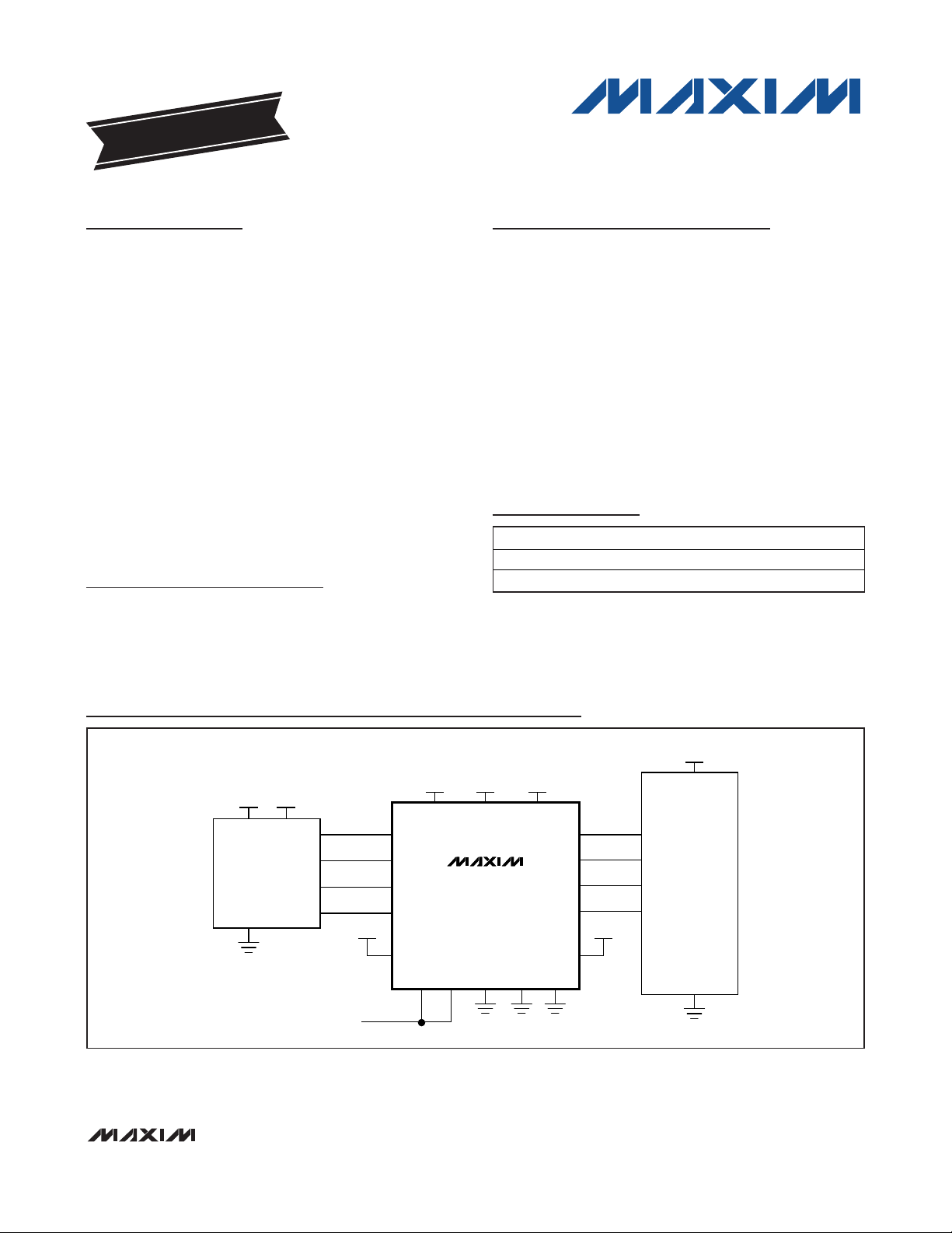
The MAX3841 is a low-power, 12.5Gbps 2 × 2 crosspoint switch IC for high-speed serial data loopback,
redundancy, and switching applications. The MAX3841
current-mode logic (CML) inputs and outputs have isolated VCCconnections to enable DC-coupled interfaces
to 1.8V, 2.5V, or 3.3V CML ICs. Fully differential signal
paths and Maxim’s second-generation SiGe technology
provide optimum signal integrity, minimizing jitter,
crosstalk, and signal skew. The MAX3841 is ideal for
serial OC-192 and 10GbE optical module, line card,
switch fabric, and similar applications.
The MAX3841 has 150mV
P-P
minimum differential input
sensitivity, and 500mV
P-P
nominal differential output
swing. Unused outputs can be powered down individually to conserve power. In addition to functioning as a 2
× 2 switch, the MAX3841 can be configured as a 2:1
multiplexer, 1:2 buffer, or dual 1:1 buffer. The MAX3841
is available in a 4mm × 4mm 24-pin thin QFN package,
and consumes only 215mW with both outputs enabled.
Applications
OC-192, 10GbE Switch/Line Cards
OC-192, 10GbE Optical Modules
System Redundancy/Self Test
Clock Fanout
Features
♦ Up to 12.5Gbps Operation
♦ Less Than 10ps
P-P
Deterministic Jitter
♦ Less Than 0.7ps
RMS
Random Jitter
♦ 1.8V, 2.5V, and 3.3V DC-Coupled CML I/O
♦ Independent Output Power-Down
♦ 4mm × 4mm Thin QFN Package
♦ -40°C to +85°C Operation
♦ +3.3V Core Supply
♦ 215mW Power Consumption (Excluding
Termination Currents)
MAX3841
12.5Gbps CML 2 ×2 Crosspoint Switch
________________________________________________________________
Maxim Integrated Products
1
Ordering Information
MAX3841
10Gbps
SERIAL
OPTICAL
MODULE
SDI+
SDI-
SDO+
SDO-
OUT1+
OUT1-
IN1+
IN1-
SEL1 SEL2 ENO1 ENO2
LOOPBACK
3.3V
V
CCVCC1OUT
VCC1IN
2.5V
2.5V
2.5V
IN2+
IN2-
OUT2+
OUT2-
SDO+
SDO-
SDI+
SDI-
VCC2IN
VCC2OUT
1.8V
1.8V
GND
10Gbps
CDR/SERDES
ASIC
3.3V
1.8V
Typical Application Circuit
19-2905; Rev 1; 3/09
EVALUATION KIT
AVAILABLE
Pin Configuration appears at end of data sheet.
+
Denotes a lead(Pb)-free/RoHS-compliant package.
*
EP = Exposed pad.
For pricing, delivery, and ordering information, please contact Maxim Direct at 1-888-629-4642,
or visit Maxim's website at www.maxim-ic.com.
PART TEMP RANGE PIN-PACKAGE
MAX3841ETG -40°C to +85°C 24 Thin QFN-EP*
MAX3841ETG+ -40°C to +85°C 24 Thin QFN-EP*
Page 2
MAX3841
12.5Gbps CML 2 ×2 Crosspoint Switch
2 _______________________________________________________________________________________
ABSOLUTE MAXIMUM RATINGS
ELECTRICAL CHARACTERISTICS
(VCC= +3.0V to +3.6V, VCC_IN = +1.71V to VCC, VCC_OUT = +1.71V to VCC, TA= -40°C to +85°C. Typical values are at VCC=
+3.3V, VCC_IN = VCC_OUT = 1.8V, T
A
= +25°C, unless otherwise noted.)
Stresses beyond those listed under “Absolute Maximum Ratings” may cause permanent damage to the device. These are stress ratings only, and functional
operation of the device at these or any other conditions beyond those indicated in the operational sections of the specifications is not implied. Exposure to
absolute maximum rating conditions for extended periods may affect device reliability.
Note 1: Guaranteed by design and characterization.
Note 2: Differential swing is defined as V
IN
= (IN_+) - (IN_-) and V
OUT
= (OUT_+) - (OUT_-). See Figure 1.
Note 3: Measured using a 0000011111 pattern at 12.5Gbps, and V
IN
= 400mV
P-P
differential.
Note 4: Measured at 9.953Gbps using a pattern of 100 ones, 2
7
- 1 PRBS, 100 zeros, 27 - 1 PRBS, and at 12.5Gbps using a ±K28.5
pattern. VCC_IN = VCC_OUT = 1.8V, and V
IN
= 400mV
P-P
differential.
Note 5: Refer to Application Note 1181:
HFAN-04.5.1: Measuring Random Jitter on a Digital Sampling Oscilloscope
.
Supply Voltage, V
CC
..............................................-0.5V to +4.0V
CML Supply Voltage (VCC_IN, VCC_OUT)...........-0.5V to +4.0V
Continuous Output Current (OUT1±, OUT2±)...................±25mA
CML Input Voltage (IN1±, IN2±)...........-0.5V to (VCC_IN + 0.5V)
LVCMOS Input Voltage (SEL1, SEL2,
ENO1, ENO2) .........................................-0.5V to (V
CC
+ 0.5V)
Continuous Power Dissipation (T
A
= +85°C)
24-Pin Thin QFN (derate 20.8mW/°C
above +85°C).............................................................1352mW
Operating Temperature Range ...........................-40°C to +85°C
Storage Temperature Range .............................-55°C to +150°C
Lead Temperature (soldering, 10s) .................................+300°C
PARAMETER SYMBOL CONDITIONS MIN TYP MAX UNITS
Core Supply Current ICC Excluding CML termination currents 65 90 mA
Data Rate (Note 1) 0 12.5 Gbps
CML Input Differential VIN AC-coupled or DC-coupled (Note 2) 150 1200 mV
CML Input Common Mode DC-coupled VCC_IN - 0.3 VCC_IN V
CML Input Termination Single ended 42.5 50 57.5
CML Input Return Los s Up to 10GHz 12 dB
CML Output Differential V
CML Output Terminat ion Single ended 42.5 50 57.5
CML Output Tran sition Time tR, tF 20% to 80% (Notes 1, 3) 30 ps
Determin istic Jitter (Notes 1, 4) 10 ps
Random Jitter VIN = 150mV
Propagation Delay Any input to output (Note 1) 100 140 ps
Channel-to-Channel Skew (Note 1) 12 ps
Output Duty-Cycle Skew 50% input duty c yc le (Notes 1, 3) 8 ps
LVCMOS Input Current IIH, IIL -10 +10 μA
LVCMOS Input High Voltage VIH 1.7 V
LVCMOS Input Low Voltage VIL 0.7 V
(Note 2) 400 500 600 mV
OUT
(Notes 1, 5) 0.3 0.7 ps
P-P
P-P
P-P
P-P
RMS
Page 3
MAX3841
12.5Gbps CML 2 ×2 Crosspoint Switch
_______________________________________________________________________________________
3
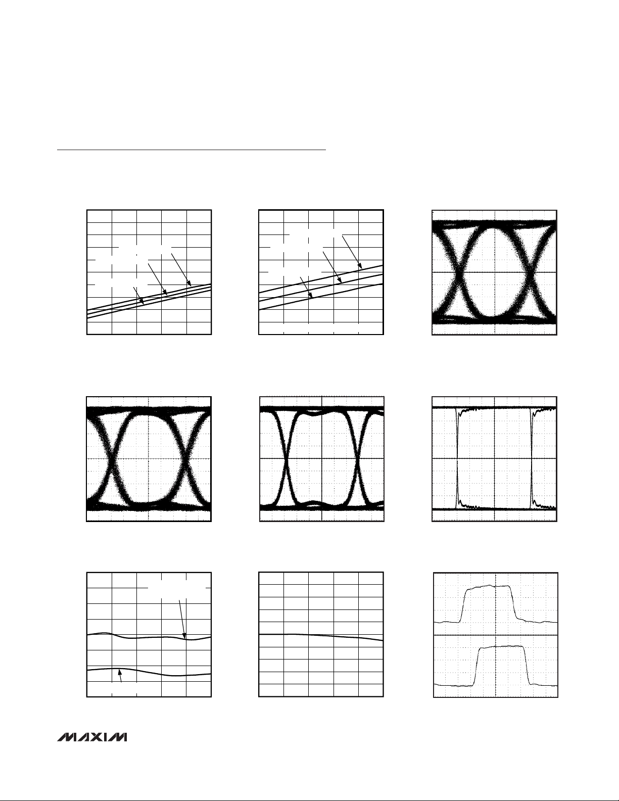
Typical Operating Characteristics
(VCC= 3.3V, VCC_IN, VCC_OUT = 1.8V, VIN= 500mV
P-P
, TA= +25°C, unless otherwise noted.)
CORE SUPPLY CURRENT vs. TEMPERATURE
(EXCLUDES CML I/O CURRENTS)
140
130
120
110
100
90
80
70
SUPPLY CURRENT (mA)
60
50
40
-40 85
0 OUTPUTS ENABLE
1 OUTPUT ENABLE
2 OUTPUTS ENABLE
TEMPERATURE (°C)
OUTPUT EYE DIAGRAM
(10.7Gbps, 2
23
- 1 PRBS)
603510-15
MAX3841 toc04
140
130
MAX3841 toc01
120
110
100
90
80
70
SUPPLY CURRENT (mA)
60
50
40
SUPPLY CURRENT vs. TEMPERATURE
(CORE PLUS CML I/O CURRENTS)
2 OUTPUTS ENABLE
1 OUTPUT ENABLE
0 OUTPUTS ENABLE
CML INPUTS AND OUTPUTS AC-COUPLED
-40 85
TEMPERATURE (°C)
OUTPUT EYE DIAGRAM
(6.25Gbps, 2
23
- 1 PRBS)
603510-15
MAX3841 toc05
MAX3841 toc02
60mV/div
OUTPUT EYE DIAGRAM
(12.5Gbps, 2
OUTPUT EYE DIAGRAM
(622Mbps, 2
23
14ps/div
23
- 1 PRBS)
- 1 PRBS)
MAX3841 toc03
MAX3841 toc06
60mV/div
16ps/div
DETERMINISTIC JITTER
vs. TEMPERATURE
16
14
12
10
8
6
DETERMINISTIC JITTER (ps)
4
2
±K28.5 AT 12.5Gbps
0
-40 85
27 - 1 PRBS + 100CIDs
TEMPERATURE (°C)
AT 10.7Gbps
6035-15 10
60mV/div
550
540
)
MAX3841 toc07
530
P-P
520
510
500
490
480
DIFFERENTIAL OUTPUT (mV
470
460
450
-40 85
28ps/div
DIFFERENTIAL OUTPUT SWING
vs. TEMPERATURE
603510-15
TEMPERATURE (°C)
60mV/div
MAX3841 toc08
IN1
OUT1
270ps/div
PROPAGATION DELAY
100ps/div
MAX3841 toc09
Page 4

MAX3841
12.5Gbps CML 2 ×2 Crosspoint Switch
4 _______________________________________________________________________________________
Pin Description
Detailed Description
The MAX3841 contains a pair of CML inputs that drive
two 2:1 multiplexers, with separate select inputs SEL1
and SEL2, providing a 2 × 2 crosspoint data path. The
outputs of the multiplexers each drive a high-performance CML output that can be disabled (powered
down) using the ENO1/ENO2 inputs. All of the data
paths are fully differential to minimize jitter, crosstalk,
and signal skew. See Figure 1 for the functional diagram.
CML Input and Output Buffers
The MAX3841 input and output buffers are terminated
with 50Ω to independent supply lines, and are also compatible with 100Ω differential terminations. (See Figures 3
and 4.) Separate power-supply connections are provided
for the core, input buffers, and output buffers to allow DCcoupling to 1.8V, 2.5V, or 3.3V CML ICs. If desired, the
CML inputs and outputs can be AC-coupled.
The CML inputs accept serial NRZ data with differential
amplitude from 150mV
P-P
to 1200mV
P-P
(see Figure 2).
The CML outputs provide 500mV
P-P
nominal differential
swing, resulting in low power consumption.
Figure 1. Functional Diagram
PIN NAME FUNCTION
1, 12 VCC +3.3V Core Supply Voltage
2, 5 VCC1IN Supply Voltage for CML Input IN1. Connect to 1.8V, 2.5V, or 3.3V.
3 IN1+ Positive Serial Data Input 1, CML
4 IN1- Negati ve Serial Data Input 1, CML
6 SEL1 Output 1 Select, LVCMOS Input. See Table 1.
7 SEL2 Output 2 Select, LVCMOS Input. See Table 1.
8, 11 VCC2IN Supply Voltage for CML Input IN2. Connect to 1.8V, 2.5V, or 3.3V.
9 IN2+ Positive Serial Data Input 2, CML
10 IN2- Negative Serial Data Input 2, CML
13, 24 GND Supply Ground
14, 17 VCC1OUT Supply Voltage for CML Output OUT1. Connect to 1.8V, 2.5V, or 3.3V.
15 OUT1- Negative Serial Data Output 1, CML
16 OUT1+ Posit ive Serial Data Output 1, CML
18 ENO1 Output 1 Enable, LVCMOS Input. See Table 1.
19 ENO2 Output 2 Enable, LVCMOS Input. See Table 1.
20, 23 VCC2OUT Supply Voltage for CML Output OUT2. Connect to 1.8V, 2.5V, or 3.3V.
21 OUT2- Negative Serial Data Output 2, CML
22 OUT2+ Posit ive Serial Data Output 2, CML
— EP
Exposed Pad. The exposed pad must be soldered to the circuit board ground for proper thermal and
electrical performance.
IN1
2
CML
1
CML
0
IN2
2
CML
MAX3841
1
CML
0
2
OUT1
ENO1
SEL1
2
OUT2
ENO2
SEL2
Page 5

Applications Information
Select and Enable Controls
The MAX3841 provides two LVCMOS-compatible
select inputs, SEL1 and SEL2. Either data input can be
connected to either or both data outputs. The MAX3841
provides two LVCMOS-compatible enable inputs,
ENO1 and ENO2, so each output can be disabled
independently. The MAX3841 can also be used as a
1:2 driver, 2:1 multiplexer, or a dual 1:1 buffer by using
the LVCMOS control inputs accordingly (see Table 1).
Power-Supply Connections
Each of the input and output power-supply connections
(VCC1IN, VCC2IN, VCC1OUT, VCC2OUT) is independent and need not be connected to the same voltage.
The input and output supplies can be connected to
1.8V, 2.5V, or 3.3V, but the core supply (VCC) must be
connected to 3.3V for proper operation.
Input and Output Interfaces
The MAX3841 inputs and outputs can be AC-coupled
or DC-coupled according to the application. If an input
or output is not used it should be terminated with 50Ω
to the correct input or output supply voltage. For more
information about interfacing with logic families, refer to
Application Note 291:
HFAN-01.0: Introduction to
LVDS, PECL, and CML
.
Package and Layout Considerations
The MAX3841 is packaged in a 4mm × 4mm 24-pin thin
QFN with exposed pad. The exposed pad provides
thermal and electrical connectivity to the IC and must
be soldered to a high-frequency ground plane. Use
multiple vias to connect the exposed pad underneath
the package to the PC board ground plane.
Use good layout techniques for the 10Gbps PC board
transmission lines, and configure the layout near the IC to
minimize impedance discontinuities. Power-supply
decoupling capacitors should be located as close as
possible to the IC.
MAX3841
12.5Gbps CML 2 ×2 Crosspoint Switch
_______________________________________________________________________________________ 5
Figure 2. Definition of Differential Voltage Swing
Figure 3. Equivalent CML Input Circuit
Figure 4. Equivalent CML Output Circuit
Table 1. Output Controls
V-
600mV
MAX
V+
(V+) - (V-)
IN_+
IN_-
1200mV
MAX
VCC_IN
MAX3841
50Ω50Ω
75mV
MIN
150mV
MIN
ENO1 ENO2 SEL1 SEL2 OUT1 OUT2
0 0 0 0 IN2 IN1
0 0 0 1 IN2 IN2
0 0 1 0 IN1 IN1
0 0 1 1 IN1 IN2
1 1 X X Disabled Disabled
VCC_OUT
50Ω 50Ω
MAX3841
OUT_+
OUT_-
Page 6

MAX3841
12.5Gbps CML 2 ×2 Crosspoint Switch
6 _______________________________________________________________________________________
Chip Information
TRANSISTOR COUNT: 950
PROCESS: SiGe BiCMOS
1
V
CC
2
VCC1IN
3
IN1+
4
IN1-
5
VCC1IN
6
SEL1
7
SEL2
8
VCC2IN
9
IN2+
10
IN2-
11
VCC2IN
12
V
CC
13
GND
14
VCC1OUT
15
OUT1-
16
OUT1+
17
VCC1OUT
18
ENO1
19
ENO2
20
VCC2OUT
21
OUT2-
22
OUT2+
23
VCC2OUT
24
GND
MAX3841
THIN QFN
*THE EXPOSED PAD OF THE QFN PACKAGE MUST BE
SOLDERED TO GROUND FOR PROPER THERMAL AND
ELECTRICAL OPERATION.
TOP VIEW
*EP
Pin Configuration
Package Information
For the latest package outline information and land patterns, go
to www.maxim-ic.com/packages
.
PACKAGE TYPE PACKAGE CODE DOCUMENT NO.
24 TQFN-EP T2444-3
21-0139
Page 7

MAX3841
12.5Gbps CML 2 ×2 Crosspoint Switch
Maxim cannot assume responsibility for use of any circuitry other than circuitry entirely embodied in a Maxim product. No circuit patent licenses are
implied. Maxim reserves the right to change the circuitry and specifications without notice at any time.
Maxim Integrated Products, 120 San Gabriel Drive, Sunnyvale, CA 94086 408-737-7600 _____________________
7
© 2009 Maxim Integrated Products Maxim is a registered trademark of Maxim Integrated Products, Inc.
Revision History
REVISION
NUMBER
0 8/03 Initial release. —
1 3/09
REVISION
DATE
DESCRIPTION
Added a lead-free package to the Ordering Information table. 1
Changed the package code from T2444-1 to T2444-3 and replaced the package
outline drawings with the Package Information table.
PAGES
CHANGED
1, 6
 Loading...