

Page 1
General Description
The MAX3840 is a dual 2 ✕2 asynchronous crosspoint
switch for SDH/SONET DWDM and other high-speed
data switching applications where serial data stream
loop-through and protection channel switching are
required. It is ideal for OC-48 systems with forward
error correction. A high-bandwidth, fully differential signal path minimizes jitter accumulation, crosstalk, and
signal skew. Each 2 ✕2 crosspoint switch can fan out
and/or multiplex up to 2.7Gbps data and 2.7GHz clock
signals. All inputs and outputs are current mode logic
(CML) compatible and easily adaptable to interface
with an AC-coupled LVPECL signal. When not used,
each CML output stage can be powered down with an
enable control to conserve power. The typical power
consumption is 460mW with all outputs enabled.
The MAX3840 is compatible with the MAX3876
2.5Gbps clock and data recovery (CDR) circuit.
The MAX3840 is available in a 32-pin exposed-pad
QFN package (5mm ✕5mm footprint) and operates
from a +3.3V supply over a temperature range of -40°C
to +85°C.
________________________Applications
SDH/SONET and DWDM Transport Systems
Add-Drop Multiplexers
ATM Switch Cores
WDM Cross-Connects
High-Speed Backplanes
Features
♦ Single +3.3V Supply
♦ 460mW Power Consumption
♦ 2ps
RMS
Random Jitter
♦ 7ps
P-P
Deterministic Jitter
♦ Power-Down Feature for Deselected Outputs
♦ CML Inputs/Outputs
♦ 6ps Channel-to-Channel Skew
♦ 100ps Output Edge Speed
♦ 5mm
✕
5mm 32 QFN or Thin QFN Package
MAX3840
+3.3V, 2.7Gbps Dual 2 ✕2 Crosspoint Switch
________________________________________________________________ Maxim Integrated Products 1
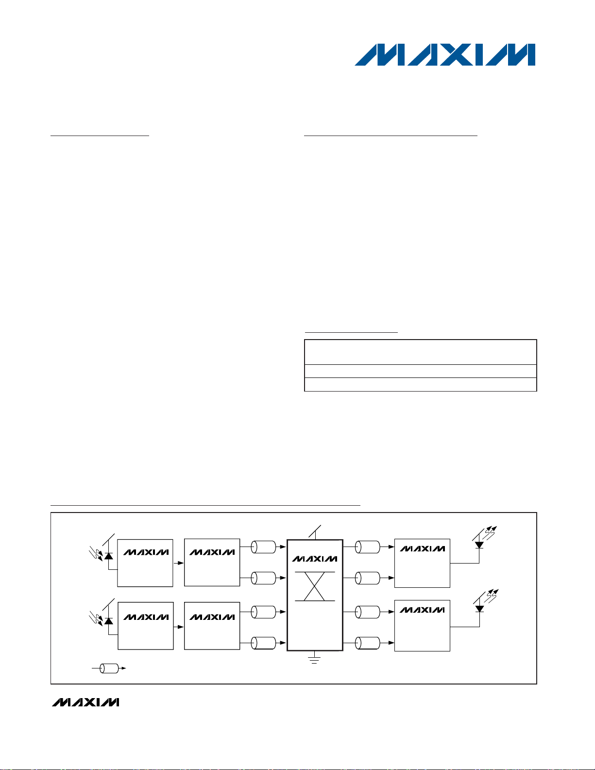
MAX3866
TIA AND LA
MAX3876
CDR
MAX3840
CROSSPOINT
SWITCH
ZO = 50Ω TRANSMISSION LINE
DATA
CLOCK
MAX3866
TIA AND LA
MAX3876
CDR
DATA
CLOCK
MAX3869
MAX3869
LASER
DRIVER
LASER
DRIVER
VCC = +3.3V
Typical Application Circuit
19-1854; Rev 5; 9/07
Ordering Information
PART
TEMP RANGE
PIN -
PK G
C O D E
MAX3840ETJ+
32 TQFN T3255-3
MAX3840EGJ
32 QFN G3255-1
Pin Configurations appear at end of data sheet.
For pricing, delivery, and ordering information, please contact Maxim Direct at 1-888-629-4642,
or visit Maxim’s website at www.maxim-ic.com.
+Denotes a lead-free package.
PA C K A G E
-40°C to +85°C
-40°C to +85°C
Page 2
MAX3840
+3.3V, 2.7Gbps Dual 2 ✕2 Crosspoint Switch
2 _______________________________________________________________________________________
ABSOLUTE MAXIMUM RATINGS
DC ELECTRICAL CHARACTERISTICS
(VCC= +3.0V to +3.6V, TA= -40°C to +85°C. Typical values are at VCC= +3.3V, TA= +25°C, unless otherwise noted.)
Stresses beyond those listed under “Absolute Maximum Ratings” may cause permanent damage to the device. These are stress ratings only, and functional
operation of the device at these or any other conditions beyond those indicated in the operational sections of the specifications is not implied. Exposure to
absolute maximum rating conditions for extended periods may affect device reliability.
Supply Voltage, VCC.............................................-0.5V to +5.0V
Input Voltage (CML) .........................(VCC - 1.0) to (V
CC
+ 0.5V)
TTL Control Input Voltage...........................-0.5V to (V
CC
+ 0.5V)
Output Currents (CML) .......................................................22mA
Continuous Power Dissipation (T
A
= +85°C)
32-Pin TQFN
(derate 21.3mW/°C above +85°C).................................1.38W
32-Pin QFN
(derate 21.3mW/°C above +85°C).................................1.38W
Operating Temperature Range ...........................-40°C to +85°C
Operating Junction Temperature Range...........-55°C to +150°C
Storage Temperature Range .............................-65°C to +160°C
Lead Temperature (soldering, 10s) .................................+300°C
PARAMETER
CONDITIONS
UNITS
Supply Current I
CC
All outputs enabled
mA
CML INPUT AND OUTPUT SPECIFICATIONS
CML Differential Output Swing RL = 50Ω to V
CC
(Figure 2)
mV
P-P
Differential Output Impedance
Ω
CML Output Common-Mode
Voltage
R
L
= 50Ω to V
CC
V
CC
- 0.2 V
CML Single-Ended Input
Voltage Range
V
IS
V
CML Differential Input Voltage
Swing
mV
P-P
CML Single-Ended Input
Impedance
42.5 50 57.5 Ω
TTL SPECIFICATIONS
TTL Input High Voltage V
IH
V
TTL Input Low Voltage V
IL
0.8 V
TTL Input High Current I
IH
µA
TTL Input Low Current I
IL
-10 +10 µA
SYMBOL
MIN TYP MAX
140 190
640 800 1000
85 100 115
VCC - 0.8 VCC + 0.5
300 2000
2.0
-10 +10
Page 3
MAX3840
+3.3V, 2.7Gbps Dual 2 ✕2 Crosspoint Switch
_______________________________________________________________________________________ 3
AC ELECTRICAL CHARACTERISTICS
(VCC= +3.0V to +3.6V, TA= -40°C to +85°C. Typical values are at VCC= +3.3V, TA= +25°C, unless otherwise noted.) (Note 1)
PARAMETER
CONDITIONS
CML Input and Output Data
Rate
2.7
CML Input and Output Clock
Rate
2.7
CML Output Rise and Fall Time tr, t
f
20% to 80% 100 136 ps
CML Output Random Jitter RJ (Note 2) 2
CML Output Deterministic Jitter DJ (Note 3)
CML Output Differential Skew t
skew1
Any differential pair
ps
CML Output Channel-toChannel Skew
t
skew2
Any two outputs
ps
Propagation Delay from Inputto-Output
t
d
ps
CML Differential Output Swing
for 2.7Gbps Input Data
RL = 50Ω to V
CC
(Note 4)
CML Differential Output Swing
for 2.7GHz Input Clock
RL = 50Ω to V
CC
(Note 5)
Note 1: AC characteristics are guaranteed by design and characterization.
Note 2: Measured with 100mV
P-P
noise (f ≤ 2MHz) on the power supply.
Note 3: Deterministic jitter (DJ) is the arithmetic sum of pattern-dependent jitter and pulse-width distortion.
Note 4: Measured with 300mV
P-P
differential 1010... data pattern driving the inputs.
Note 5: Measured with 300mV
P-P
differential clock at 2.7GHz driving the inputs.
SYMBOL
MIN TYP MAX
720ps
725
15 40
185
600 mV
520 mV
UNITS
Gbps
GHz
ps
RMS
-
P-P
P-P
Page 4

MAX3840
+3.3V, 2.7Gbps Dual 2 ✕2 Crosspoint Switch
4 _______________________________________________________________________________________
SUPPLY CURRENT vs. TEMPERATURE
MAX3840 toc01
0
20
60
40
120
140
100
80
160
SUPPLY CURRENT (mA)
-50 -10 10-30
30
50 70 90
TEMPERATURE (°C)
4 OUTPUTS ENABLED
3 OUTPUTS ENABLED
2 OUTPUTS ENABLED
1 OUTPUT ENABLED
0 OUTPUTS ENABLED
CML DIFFERENTIAL VOLTAGE
MAX3840 toc02
200
250
400
350
300
650
600
700
750
550
500
450
800
CML DIFFERENTIAL VOLTAGE (mV
P-P
)
-50 -10 10-30
30
50 70 90
TEMPERATURE (°C)
0
4
2
8
6
12
10
14
18
16
20
-50 -10-30 10 30 50 70 90
CHANNEL-TO-CHANNEL SKEW
vs. TEMPERATURE
MAX3840 toc04
TEMPERATURE (°C)
TMIE (ps)
CHANNEL A
CHANNEL B
2.7Gbps EYE DIAGRAM
MAX3840 toc03
54ps/div
150mV/div
INPUT = 2
23
- 1PRBS
Typical Operating Characteristics
(VCC= +3.3V, TA= +25°C, unless otherwise noted.)
Page 5

MAX3840
+3.3V, 2.7Gbps Dual 2 ✕2 Crosspoint Switch
_______________________________________________________________________________________ 5
Pin Description
PIN NAME FUNCTION
1 ENB1 Channel B1 Output Enable, TTL Input. A TTL low input powers down B1 output stage.
2 DIB1+ Channel B1 Positive Signal Input, CML
3 DIB1- Channel B1 Negative Signal Input, CML
4 ENB0 Channel B0 Output Enable, TTL Input. A TTL low input powers down B0 output stage.
5 SELB0 Channel B0 Output Select, TTL Input. See Table 1.
6 DIB0+ Channel B0 Positive Signal Input, CML
7 DIB0- Channel B0 Negative Signal Input, CML
8 SELB1 Channel B1 Output Select, TTL Input. See Table 1.
9, 24 GND Supply Ground
10, 13, 16, 17,
20, 23
V
CC
Positive Supply
11 DOB0- Channel B0 Negative Output, CML
12 DOB0+ Channel B0 Positive Output, CML
14 DOB1- Channel B1 Negative Output, CML
15 DOB1+ Channel B1 Positive Output, CML
18 DOA1- Channel A1 Negative Output, CML
19 DOA1+ Channel A1 Positive Output, CML
21 DOA0- Channel A0 Negative Output, CML
22 DOA0+ Channel A0 Positive Output, CML
25 SELA1 Channel A1 Output Select, TTL Input. See Table 1.
26 DIA0+ Channel A0 Positive Signal Input, CML
27 DIA0- Channel A0 Negative Signal Input, CML
28 SELA0 Channel A0 Output Select, TTL Input. See Table 1.
29 ENA0 Channel A0 Output Enable, TTL Input. A TTL low input powers down A0 output stage.
30 DIA1+ Channel A1 Positive Signal Input, CML
31 DIA1- Channel A1 Negative Signal Input, CML
32 ENA1 Channel A1 Output Enable, TTL Input. A TTL low input powers down A1 output stage.
EP Exposed Pad
Ground. The exposed pad must be soldered to the circuit board ground for proper
electrical and thermal operation.
Page 6

MAX3840
+3.3V, 2.7Gbps Dual 2 ✕2 Crosspoint Switch
6 _______________________________________________________________________________________
_______________ Detailed Description
The block diagram in Figure 1 shows the MAX3840
architecture. The SELA_ and SELB_ pins control the routing of the signals through the crosspoint switch. Each
output of the crosspoint switch drives a CML output driver. Each of the outputs, DOA_ and DOB_, is enabled or
disabled by the respective ENA_ and ENB_ pins.
CML Inputs and Outputs
CML is used to simplify high-speed interfacing. Onchip input and output terminations minimize the number
of external components required while improving signal
integrity. The CML output signal swing is small, resulting in lower power consumption. The internal 50Ω input
and output terminations minimize reflections and eliminate the need for external terminations.
ROUTING CONTROLS OUTPUT CONTROLS OUTPUT SIGNALS
SELA0/SELB0
Signal at DOA0/DOB0 Signal at DOA1/DOB1
0 0 1 1 DIA0/DIB0 DIA0/DIB0
0 1 1 1 DIA0/DIB0 DIA1/DIB1
1 0 1 1 DIA1/DIB1 DIA0/DIB0
1 1 1 1 DIA1/DIB1 DIA1/DIB1
X X 0 0 Power Down Power Down
Table 1. Output Routing
DOA0+
0
1
0
1
DOA0ENA0
SELA0
CML
CML
DOA1+
DIA0-
DIA0+
DOA1ENA1
SELA1
CML
DIA1-
DIA1+
DOB0+
0
1
0
1
DOB0ENB0
SELB0
CML
DOB1+
DIB0-
DIB0+
DOB1ENB1
SELB1
CML
DIB1-
DIB1+
CML
CML
CML
320mV MIN
CML+
CML-
(CML+) - (CML-)
500mV
MAX
1000mV
MAX
640mV
MIN
Figure 1. Functional Block Diagram Figure 2. CML Output Levels
SELA1/SELB1 ENA0/ENA1 ENB0/ENB1
Page 7

MAX3840
+3.3V, 2.7Gbps Dual 2 ✕2 Crosspoint Switch
_______________________________________________________________________________________ 7
Applications Information
Interfacing PECL Inputs and
Outputs to the MAX3840
For information on interfacing with CML, refer to Maxim
Application Note HFAN-01.0, Introduction to LVDS,
PECL, and CML.
Layout Techniques
For best performance, use good high-frequency layout
techniques, filter VCCsupplies, and keep ground connections short. Use multiple vias where possible. Also,
use controlled-impedance transmission lines to interface with the MAX3840 data inputs and outputs.
___________________ Interface Models
Figure 3 shows the interface model for the CML inputs,
and Figure 4 shows the model for CML outputs.
MAX3840
DIA0+
50Ω
DIA0-
V
CC
V
CC
V
CC
50Ω
Figure 3. CML Input Model
MAX3840
DOA0+
DOA0-
V
CC
50Ω50Ω
Figure 4. CML Output Model
Page 8

Chip Information
TRANSISTOR COUNT: 1200
PROCESS: Bipolar (SiGe)
32
31
30
29
28
27
26
ENA1
DIA1-
DIA1+
ENA0
SELA0
DIA0-
DIA0+
25 SELA1
9
10
11
12
13
14
15
GND
V
CC
DOB0-
DOB0+
V
CC
DOB1-
DOB1+
16V
CC
17
18
19
20
21
22
23
V
CC
DOA1-
DOA1+
V
CC
DOA0-
DOA0+
V
CC
8
7
6
5
4
3
2
SELB1
NOTE: THE EXPOSED PAD MUST BE SOLDERED
TO THE SUPPLY GROUND.
DIB0-
DIB0+
SELB0
ENB0
DIB1-
DIB1+
MAX3840
QFN
1ENB1
24 GND
TOP VIEW
Pin Configurations
32
31
30
29
28
27
26
ENA1
DIA1-
DIA1+
ENA0
SELA0
DIA0-
DIA0+
25
SELA1
9
10
11
12
13
14
15
GND
V
CC
DOB0-
DOB0+
V
CC
DOB1-
DOB1+
16
V
CC
17181920212223
VCCDOA1-
DOA1+
VCCDOA0-
DOA0+
V
CC
8765432
SELB1
NOTE: THE EXPOSED PAD MUST BE SOLDERED
TO THE SUPPLY GROUND.
DIB0-
DIB0+
SELB0
ENB0
DIB1-
DIB1+
MAX3840
THIN QFN
1
ENB1
24
GND
TOP VIEW
+
MAX3840
+3.3V, 2.7Gbps Dual 2 ✕2 Crosspoint Switch
Maxim cannot assume responsibility for use of any circuitry other than circuitry entirely embodied in a Maxim product. No circuit patent licenses are
implied. Maxim reserves the right to change the circuitry and specifications without notice at any time.
8 _____________________Maxim Integrated Products, 120 San Gabriel Drive, Sunnyvale, CA 94086 408-737-7600
© 2007 Maxim Integrated Products is a registered trademark of Maxim Integrated Products, Inc.
Package Information
For the latest package outline information, go to
www.maxim-ic.com/packages
.
PACKAGE TYPE DOCUMENT NO.
32 QFN 21-0091
32 TQFN 21-0140
Revision History
Rev 1; 11/01: Corrected specification.
Rev 2; 5/03: Added package code (page 1); updated package drawing (page 10).
Rev 3; 5/05: Added lead-free package (pages 1, 2, 8, 11, 12).
Rev 4; 12/05: Changed input voltage swing from 1.5V
P-P
(max) to 2.0V
P-P
(max).
Rev 5; 9/07: Added two AC amplitude specifications to increase test coverage for 2.5Gbps and 2.7GHz
clock inputs (page 3); removed package drawings and added package table (page 8).
 Loading...