

19-0396; Rev. 0; 5/95
Low-Voltage, 8-Channel/Dual 4-Channel
Multiplexers with Latchable Inputs
_______________General Description
The MAX382/MAX384 are low-voltage, CMOS, 1-of-8
and dual 4-channel muxes with latchable digital inputs.
They feature low-voltage operation from a +2.7V to
+16.5V single supply and from ±3V to ±8V dual supplies. Pin compatible with the DG428/DG429, these
muxes offer low on-resistance (100Ω max) matched to
within 4Ω max between channels. Additional features
include off leakage less than 2.5nA at +85°C and guaranteed low charge injection (10pC max). ESD protection is greater than 2000V per Method 3015.7.
____________________________Features
♦ Pin-Compatible with Industry-Standard
DG428/DG429, DG528/DG529, MAX368/MAX369
♦ Single-Supply Operation (+2.7V to +16.5V)
Bipolar Supply Operation (±3V to ±8V)
♦ Low Power Consumption (<300µW)
♦ Low On-Resistance, 100Ω max
♦ Guaranteed On-Resistance Match Between
Channels, 4Ω max
♦ Low Leakage, 2.5nA at +85°C
♦ TTL/CMOS-Logic Compatible
________________________Applications
Battery-Operated Systems
Audio Signal Routing
Low-Voltage Data-Acquisition Systems
Sample-and-Hold Circuits
Automatic Test Equipment
______________Ordering Information
PART
MAX382CPN
MAX382CWN
MAX382C/D 0°C to +70°C
MAX382EPN
MAX382EWN -40°C to +85°C
MAX382EJN
MAX382MJN -55°C to +125°C
Ordering Information continued on last page.
* Contact factory for dice specifications.
** Contact factory for package availability.
TEMP. RANGE PIN-PACKAGE
0°C to +70°C
0°C to +70°C
-40°C to +85°C 18 Plastic DIP
-40°C to +85°C 18 CERDIP**
18 Plastic DIP
18 Wide SO
Dice*
18 Wide SO
18 CERDIP**
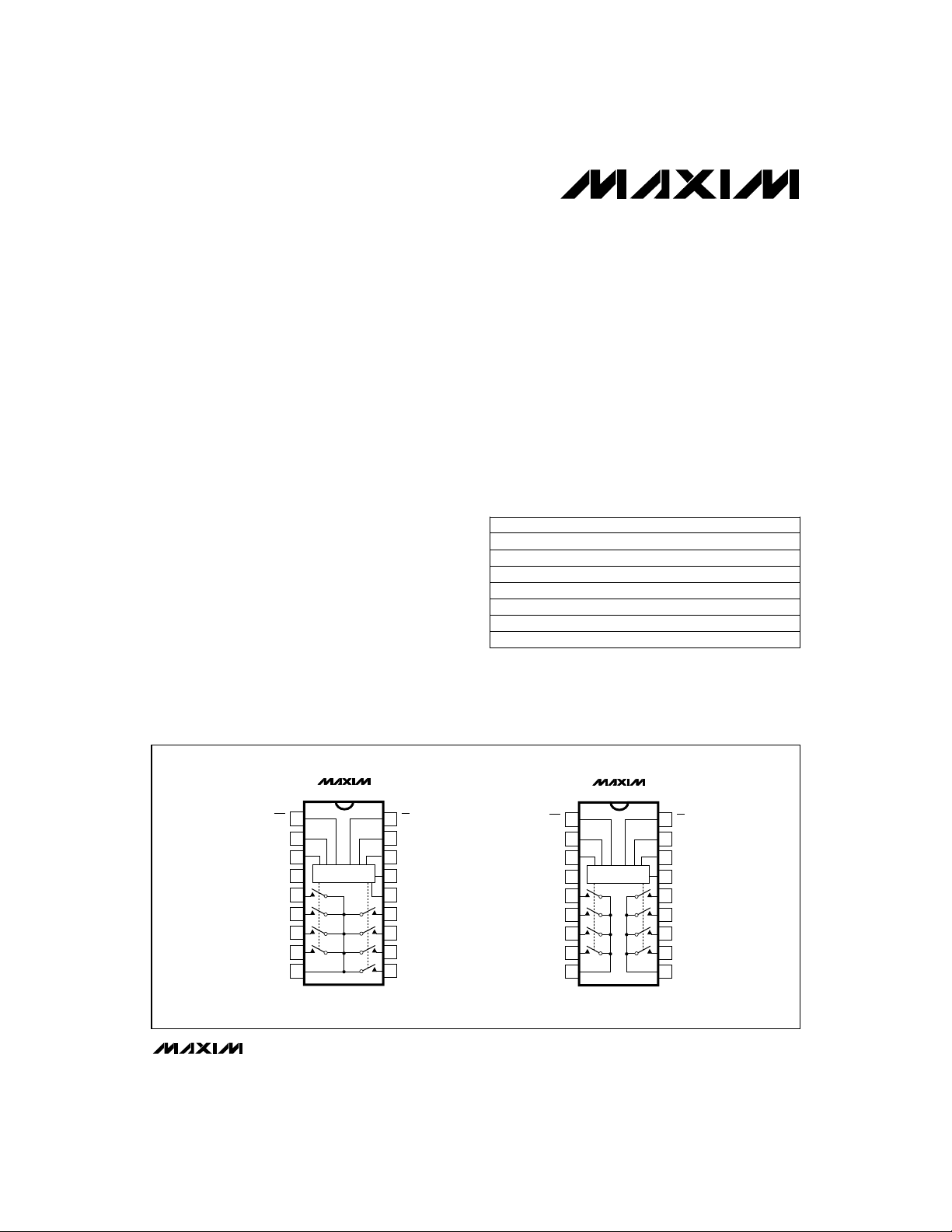
__________________________________________________________Pin Configurations
MAX382/MAX384
TOP VIEW
MAX382
1
WR
2
A0
3
EN
VN01
N02
N03
N04
COM
________________________________________________________________
LOGIC
4
5
6
7
8
9
DIP/SO
18
RS
A1
17
A2
16
GND
15
14
V+
N05
13
N06
12
N07
11
N08
10
WR
A0
EN
VN01A
N02A
N03A
N04A
COMA
MAX384
1
2
3
LOGIC
4
5
6
7
8
9
DIP/SO
Maxim Integrated Products
Call toll free 1-800-998-8800 for free samples or literature.
18
RS
A1
17
GND
16
V+
15
14
N01B
N02B
13
N03B
12
N04B
11
COMB
10
1
Low-Voltage, 8-Channel/Dual 4-Channel
Multiplexers with Latchable Inputs
ABSOLUTE MAXIMUM RATINGS
Voltage Referenced to GND
V+.......................................................................-0.3V to +17V
V-........................................................................+0.3V to -17V
V+ to V-...............................................................-0.3V to +17V
Voltage into Any Terminal (Note 1).........(V- - 2V) to (V+ + 2V) or
30mA (whichever occurs first)
Current into Any Terminal ...................................................30mA
Peak Current, Any Terminal
(pulsed at 1ms, 10% duty cycle max) ..........................100mA
Continuous Power Dissipation (T
Plastic DIP (derate 11.11mW/°C above +70°C) ..........889mW
Wide SO (derate 9.52mW/°C above +70°C)................762mW
CERDIP (derate 10.53mW/°C above +70°C)...............842mW
Operating Temperature Ranges
MAX38_C_ N.......................................................0°C to +70°C
MAX38_E_ N....................................................-40°C to +85°C
MAX38_MJN..................................................-55°C to +125°C
Storage Temperature Range.............................-65°C to +150°C
Lead Temperature (soldering, 10sec).............................+300°C
Note 1: Signals on any terminal exceeding V+ or V- are clamped by internal diodes. Limit forward current to maximum current ratings.
Stresses beyond those listed under “Absolute Maximum Ratings” may cause permanent damage to the device. These are stress ratings only, and functional
operation of the device at these or any other conditions beyond those indicated in the operational sections of the specifications is not implied. Exposure to
absolute maximum rating conditions for extended periods may affect device reliability.
= +70°C)
A
MAX382/MAX384
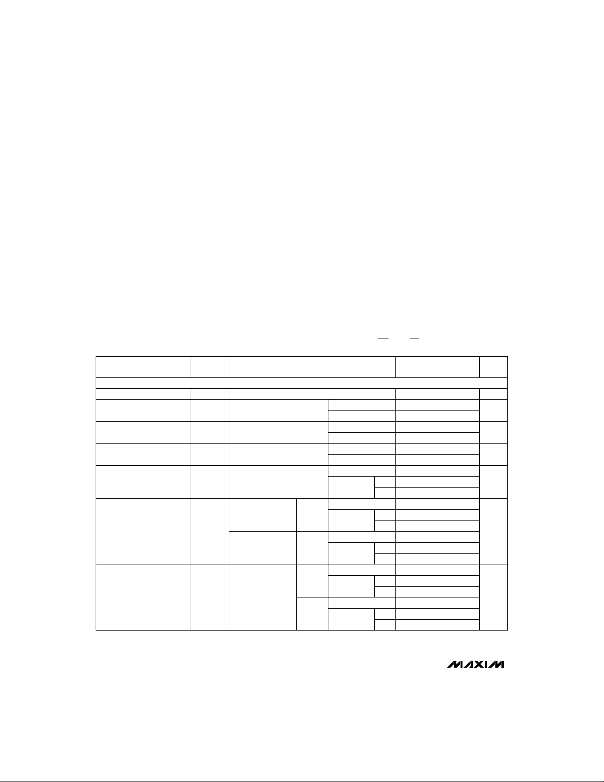
ELECTRICAL CHARACTERISTICS—Dual Supplies
(V+ = +5V ±10%, V- = -5V ±10%, GND = 0V, V
unless otherwise noted.)
SYMBOLPARAMETER
SWITCH
Analog Signal Range
Channel On-Resistance
On-Resistance Matching
Between Channels (Note 4)
On-Resistance Flatness
(Note 5)
NO-Off Leakage Current
(Note 6)
COM-Off Leakage Current
(Note 6)
COM-On Leakage Current
(Note 6)
, V
COM
R
ON
∆R
ON
R
FLAT(ON)
I
NO(OFF)
I
COM(OFF)
I
COM(ON)
NO
= V
ENH
= 2.4V, V
A_H
(Note 3)
INO= 1mA, V
INO= 1mA, V
V+ = 5V, V- = -5V
INO= 1mA, V
V+ = 5V, V- = -5V
VNO= ±4.5V, V
V+ = 5.5V, V- = -5.5V
V
= ±4.5V,
COM
±
V
= 4.5V,
NO
V+ = 5.5V, V- = -5.5V
= ±4.5V,
V
COM
±
V
= 4.5V,
NO
V+ = 5.5V, V- = -5.5V
V
= ±4.5V,
COM
V
= 4.5V,
NO
COM
COM
COM
COM
= ±3.5V
= ±3.5V,
= ±3V,
A_L
CONDITIONS
±
= 4.5V,
MAX382
MAX384
MAX382
MAX384
= V
= 0.8V, WR = 0V, RS = 2.4V, TA= T
ENL
MIN TYP MAX
TA= +25°C
TA= T
MIN
to T
MAX
TA= +25°C
TA= T
MIN
to T
MAX
TA= +25°C
TA= T
TA= +25°C
TA= T
to T
TA= +25°C
TA= T
to T
TA= +25°C
TA= T
to T
TA= +25°C
TA= T
to T
TA= +25°C
TA= T
to T
MAX
MAX
MAX
MAX
MAX
MIN
MIN
MIN
MIN
MIN
MIN
to T
MAX
C, E
M
C, E
M
C, E
M
C, E
M
C, E
M
-0.1 0.1
-1.0 1.0
-10 10
-0.2 0.2
-2.5 2.5
-20 20
-0.1 0.1
-1.5 1.5
-10 10
-0.4 0.4
-5 5
-40 40
-0.2 0.2
-2.5 2.5
-20 20
(Note 2)
60 100
125
10
13
to T
MIN
UNITS
4
6
nA
nA
nA
MAX
VV- V+V
Ω
Ω
Ω
,
2 _______________________________________________________________________________________
Low-Voltage, 8-Channel/Dual 4-Channel
Multiplexers with Latchable Inputs
ELECTRICAL CHARACTERISTICS—Dual Supplies (continued)
(V+ = +5V ±10%, V- = -5V ±10%, GND = 0V, V
unless otherwise noted.)
SYMBOLPARAMETER
DIGITAL LOGIC INPUT
Logic High Input Voltage
Logic Low Input Voltage TA= T
Input Current with
Input Voltage High
Input Current with
Input Voltage Low
A_H
A_L
A_H
A_L
, V
, V
, I
, I
ENH
ENL
ENH
ENL
SUPPLY
AX, EN Data Hold Time
Reset Pulse Width ns100Figure 6, V+ = 5V TA= +25°C
t
H
t
RS
DYNAMIC
Transition Time
Break-Before-Make Interval
Enable Turn-On Time
Enable Turn-Off Time
Write Turn-On Time
Reset Turn-Off Time
Charge Injection (Note 3)
Off Isolation (Note 7)
Crosstalk Between Channels
Logic Input Capacitance
NO-Off Capacitance
COM-Off Capacitance pF
COM-On Capacitance pF
TRANS
OPEN
t
ON(EN)
t
OFF(EN)
t
ON(WR)
t
OFF(RS)
CTE
ISO
CT
NO(OFF)
C
COM(OFF)
C
COM(ON)
IN
MINIMUM INPUT TIMING REQUIREMENTS
Write Pulse Width Figure 5 TA= +25°C
AX, EN Data Setup Time Figure 5 TA= +25°C
W
S
= V
ENH
= 2.4V, V
A_L
A_H
CONDITIONS
V
A_H
A_H
= 2.4V, V
= 2.4V, V
A_L
A_L
= 0.8V µA-0.1 0.1I
= 0.8V
VEN= VA= 0V/V+,
V+ = 5.5V, V- = -5.5V
VEN= VA= 0V/V+,
V+ = 5.5V, V- = -5.5V
Figure 5
Figure 1
Figure 2
Figure 3
Figure 3
Figure 4
Figure 6
CL= 100pF, VNO= 0V
VEN= 0V, RL= 1kΩ, f = 100kHz
VEN= 2.4V, f = 100kHz,
V
= 1V
GEN
, RL= 1kΩ
p-p
f = 1MHz
f = 1MHz, VEN= V
f = 1MHz,
VEN= V
COM
= 0V
f = 1MHz,
VEN= V
COM
= 0V
COM
= 0V
MAX382
MAX384
MAX382
MAX384
= V
= 0.8V, WR = 0V, RS = 2.4V, TA= T
ENL
MIN TYP MAX
TA= T
MIN
MIN
to T
to T
MAX
MAX
-0.1 0.1I
TA= +25°C
TA= T
MIN
to T
MAX
TA= +25°C
TA= +25°C
TA= +25°C
TA= T
MIN
to T
MAX
TA= +25°C
TA= T
MIN
to T
MAX
TA= +25°C
TA= T
MIN
to T
MAX
TA= +25°C
TA= T
MIN
to T
MAX
TA= +25°C
TA= +25°C
TA= +25°C
TA= +25°C
TA= +25°C
TA= +25°C
TA= +25°C
MIN
(Note 2)
100 150
250
80 150
250
150
250
150
250
40
20
54
34
to T
UNITS
V2.4V
V0.8V
µAV
V±2.4 ±8V+, V-Power-Supply Range
µA-1 1I+Positive Supply Current
µA-1 1I-Negative Supply Current
ns100
ns100 275t
ns020t
ns
ns
ns
ns
pC25V
dB-75V
dB-92V
pF8C
pF11C
ns100t
ns100t
MAX382/MAX384
,
MAX
_______________________________________________________________________________________ 3
Low-Voltage, 8-Channel/Dual 4-Channel
Multiplexers with Latchable Inputs
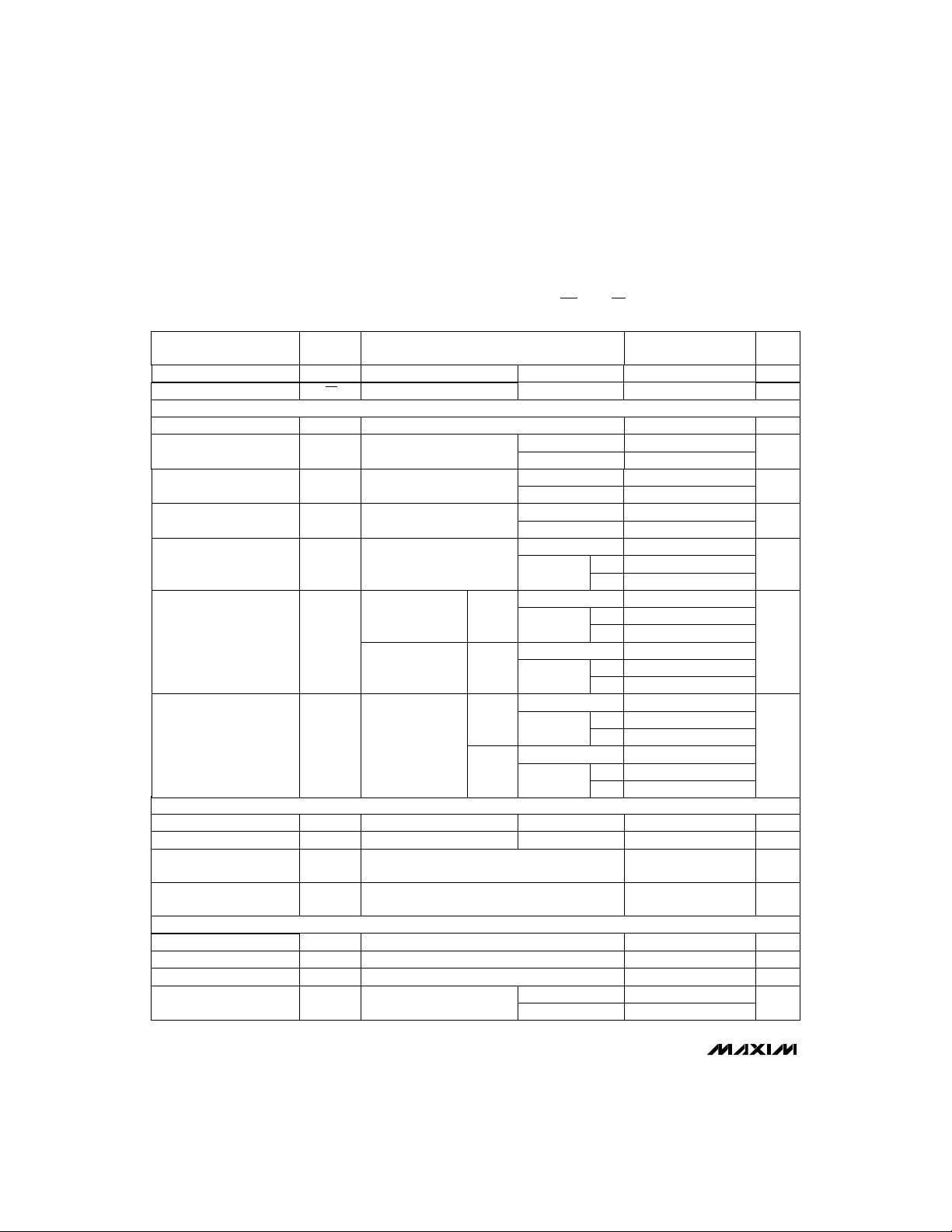
ELECTRICAL CHARACTERISTICS—Single +5V Supply
(V+ = +5V ±10%, V- = 0V, GND = 0V, V
otherwise noted.)
A_H
= V
ENH
= 2.4V, V
A_L
= V
= 0.8V, WR = 0V, RS = 2.4V, TA= T
ENL
MIN
to T
MAX
, unless
PARAMETER SYMBOL
AX, EN Data Hold Time t
Reset Pulse Width
SWITCH
SWITCH
On-Resistance R
On-Resistance Matching
Between Channels (Note 4)
MAX382/MAX384
On-Resistance Flatness R
NO-Off Leakage Current
(Note 8)
COM-Off Leakage Current
(Note 8)
COM-On Leakage Current
(Note 8)
DIGITAL LOGIC INPUT
DIGITAL LOGIC INPUT
Logic High Input Voltage VH, V
Logic Low Input Voltage VL, V
Input Current with
Input Voltage High
Input Current with
Input Voltage Low
SUPPLY
SUPPLY
H
RS
, V
COM
ON
∆R
ON
FLAT
I
NO(OFF)
I
COM(OFF)
I
COM(ON)
ENH
ENL
IH, I
ENH
IL, I
ENL
NO
Figure 5
TA= +25°C
TA= +25°C
(Note 3)Analog Signal Range V
INO= 1mA, V
V+ = 4.5V
INO= 1mA, V
V+ = 4.5V
INO= 1mA; V
V+ = 5V
VNO= 4.5V, V
V+ = 5.5V
V
= 4.5V,
COM
V
= 0V,
NO
V+ = 5.5V
V
= 4.5V,
COM
V
= 0V,
NO
V+ = 5.5V
= 3.5V,
COM
= 3.5V,
COM
= 3V, 2V, 1V;
COM
COM
= 0V,
MAX382
MAX384
TA= +25°C
TA= T
MIN
TA= +25°C
TA= T
MIN
TA= +25°C
TA= T
MIN
TA= +25°C
TA= T
MIN
to T
MAX
TA= +25°C
TA= T
MIN
to T
MAX
TA= +25°C
TA= T
MIN
to T
MAX
to T
to T
to T
TA= +25°C
V
= 4.5V,
COM
V
= 4.5V,
NO
V+ = 5.5V
MAX382
MAX384
TA= T
MIN
to T
MAX
TA= +25°C
TA= T
MIN
to T
MAX
TA= T
MIN
TA= T
MIN
to T
to T
VH= 2.4V, VL= 0.8V µA
MIN TYP MAX
(Note 2)
100 ns
100
V- V+ V
MAX
MAX
MAX
-0.1 0.1
C, E
-1.0 1.0
M
-10 10
-0.2 0.2
C, E
-2.5 2.5
M
-20 20
-0.2 0.2
C, E
-1.5 1.5
M
-10 10
-0.4 0.4
C, E
M
-5 5
-40 40
-0.2 0.2
C, E
-2.5 2.5
M
-20 20
MAX
MAX
2.4 V
-0.1 0.1 µAVH= 2.4V, VL= 0.8V
-0.1 0.1
150 225
10 16
15 20
Power-Supply Range 2.4 15 V
Positive Supply Current I+ -1.0 1.0 µA
Negative Supply Current I- -1.0 1.0 µA
I
GND Supply Current
VEN= VA= 0V, V+; V+ = 5.5V; V- = 0V
VEN= VA= 0V, V+; V+ = 5.5V; V- = 0V
VEN= V+, 0V; VA= 0V;
I
GND
V+ = 5.5V; V- = 0V
TA= +25°C
TA= T
MIN
to T
MAX
-1.0 1.0
-1.0 1.0
280
10
12
0.8
UNITSCONDITIONS
nsFigure 6, V+ = 5Vt
Ω
Ω
Ω
nA
nA
nA
V
µA
4 _______________________________________________________________________________________

Low-Voltage, 8-Channel/Dual 4-Channel
Multiplexers with Latchable Inputs
ELECTRICAL CHARACTERISTICS—Single +5V Supply (continued)
(V+ = +5V ±10%, V- = 0V, GND = 0V, V
otherwise noted.)
SYMBOLPARAMETER
DYNAMIC
Transition Time
Break-Before-Make Interval
Enable Turn-On Time
(Note 3)
Enable Turn-Off Time
(Note 3)
Write Turn-On Time
(Note 3)
Reset Turn-Off Time
(Note 3)
TRANS
t
OPEN
t
ON(EN)
t
OFF(EN)
t
ON(WR)
t
OFF(RS)
V
CTE
= V
ENH
= 2.4V, V
A_H
Figure 1, VNO= 3V
Figure 2 (Note 3)
Figure 3
Figure 3
Figure 4
Figure 4
Figure 7, CL= 100pF,
VNO= 0V
= V
A_L
ENL
CONDITIONS
= 0.8V, WR = 0V, RS = 2.4V, TA= T
MIN TYP MAX
(Note 2)
TA= +25°C
TA= +25°C
TA= T
MIN
TA= +25°C
TA= T
MIN
to T
to T
MAX
MAX
130 200
80 200
TA= +25°C
TA= T
MIN
to T
MAX
TA= +25°C
TA= T
MIN
to T
MAX
TA= +25°C
MIN
to T
275
275
200
275
200
275
MAX
, unless
UNITS
ns90 280t
ns540
ns
ns
ns
ns
pC1.5 5Charge Injection (Note 3)
pC
ELECTRICAL CHARACTERISTICS—Single +3V Supply
(V+ = +3V ±10%, V- = 0V, GND = 0V, V
otherwise noted.)
SYMBOLPARAMETER
SWITCH
Analog Signal Range
On-Resistance
ANALOG
R
ON
DYNAMIC
Transition Time (Note 3)
Enable Turn-On Time
(Note 3)
Enable Turn-Off Time
(Note 3)
Charge Injection
(Note 3)
Note 2: The algebraic convention, where the most negative value is a minimum and the most positive value a maximum, is used in this data sheet.
Note 3: Guaranteed by design.
Note 4: ∆R
Note 5: Flatness is defined as the difference between the maximum and minimum value of on-resistance as measured over the specified analog signal
Note 6: Leakage parameters are 100% tested at maximum rated hot operating temperature, and guaranteed by correlation at +25°C.
Note 7: Worst-case isolation is on channel 4 because of its proximity to the COM pin. Off isolation = 20log V
Note 8: Leakage testing at single supply is guaranteed by correlation testing with dual supplies.
= RON(max) - RON(min).
ON
ranges, i.e., V
NO
= 3V to 0V and 0V to -3V.
TRANS
ON(EN)
OFF(EN)
ON(WR)
OFF(RS)
CTE
= V
ENH
= 2.4V, V
A_H
(Note 3)
INO= 1mA, V
V+ = 3V
COM
Figure 1, VIN= 2.4V,
V
= 1.5V, V
N01
Figure 3, V
V
Figure 3, V
V
INL
INL
= 0V, V
= 0V, V
INH
N01
INH
N01
Figure 7, CL= 100pF,
VNO= 0V
A_L
CONDITIONS
= 1.5V,
= 0V
N08
= 2.4V,
= 1.5V
= 2.4V,
= 1.5V
= V
= 0.8V, WR = 0V, RS = 2.4V, TA= T
ENL
TA= +25°C
TA= T
MIN
to T
MAX
TA= +25°C
TA= +25°C
TA= +25°C
TA= +25°CWrite Turn-On Time (Note 3) Figure 4
TA= +25°CReset Turn-Off Time (Note 3) Figure 4
TA= +25°C
COM/VNO
MIN
MIN TYP MAX
(Note 2)
230 375
75 400t
, V
= output, VNO= input to off switch.
COM
to T
425
MAX
, unless
UNITS
ns230 575t
ns200 500t
ns
ns200 500t
ns75 400t
pC15V
MAX382/MAX384
VV- V+V
Ω
_______________________________________________________________________________________ 5

Low-Voltage, 8-Channel/Dual 4-Channel
Multiplexers with Latchable Inputs
__________________________________________Typical Operating Characteristics
(TA = +25°C, unless otherwise noted.)
ON-RESISTANCE vs. V
(DUAL SUPPLIES)
110
100
90
80
(Ω)
70
ON
R
60
50
40
MAX382/MAX384
30
-5 -3 1
-1 3
V
ON-RESISTANCE vs. V
AND TEMPERATURE
180
160
140
120
(Ω)
ON
100
R
80
60
40
02
(SINGLE SUPPLY)
V+ = 5V
V- = 0V
TA = +125°C
T
153
V
COM
COM
V± = ±3V
V± = ±5V
COM
TA = -55°C
4
5-4 0-2 2 4
(V)
COM
TA = +85°C
= +25°C
A
(V)
CHARGE INJECTION vs. V
5
(pC)
j
Q
V+ = 5V
V- = -5V
110
100
MAX398/9 TOC1
(Ω)
ON
R
1000
MAX398/9 TOC4
OFF-LEAKAGE (pA)
COM
V+ = 5V
V- = 0V
ON-RESISTANCE vs. V
AND TEMPERATURE
(DUAL SUPPLIES)
V+ = 5V
V- = -5V
90
V+ = 5.5V
V- = -5.5V
MAX398/9 TOC7
TA = +125°C
TA = +85°C
TA = +25°C
TA = -55°C
-1 3
V
COM
OFF-LEAKAGE vs.
TEMPERATURE
TEMPERATURE (°C)
80
70
60
50
40
30
-5 -3 1
100
10
1
0.1
-50 12525-25 0 7550 100
(V)
COM
10
1
I+, I- (nA)
MAX398/9 TOC2
5-4 0-2 2 4
MAX398/9 TOC5
V+ = 5V
V- = -5V
V
EN
(Ω)
ON
R
10,000
ON-LEAKAGE (pA)
= VA = 0V, 5V
ON-RESISTANCE vs. V
300
275
250
225
200
175
150
125
100
75
50
1000
100
10
1
0.1
SUPPLY CURRENT vs.
TEMPERATURE
(SINGLE SUPPLY)
V- = 0V
V+ = 3V
02
153
V
(V)
COM
ON-LEAKAGE vs.
TEMPERATURE
V+ = 5.5V
V- = -5.5V
-50 12525-25 0 7550 100
TEMPERATURE (°C)
I+
I-
V+ = 5V
MAX398/9 TOC8
COM
MAX398/9 TOC3
4
MAX398/9 TOC6
-5
-5 -3 1
-1 305-4 0-2 2 4
V
(V)
COM
0.1
-50 12525-25 0 7550 100
TEMPERATURE (°C)
6 _______________________________________________________________________________________

Low-Voltage, 8-Channel/Dual 4-Channel
Multiplexers with Latchable Inputs
______________________________________________________________Pin Description
PIN
MAX382 MAX384
1 WR WRITE Logic Input
2, 16, 17 A0, A2, A1 Address Logic Inputs (see
—
3 3 EN Enable Logic Input (see
4 4 V- Negative Supply Voltage Input. Connect to GND for single-supply operation.
5–8 — NO1–NO4 Analog Signal Inputs—bidirectional
— 5–8 NO1A–NO4A Analog Signal Inputs—bidirectional
9 — COM Analog Signal Output—bidirectional
— 9, 10 COMA, COMB Analog Signal Outputs—bidirectional
10–13 — NO8–NO5 Analog Signal Inputs—bidirectional
— 11–14 NO4B–NO1B Analog Signal Inputs—bidirectional
14 15 V+ Positive Supply Voltage Input
15 16 GND Ground
18 18 RS RESET Logic Input
*Analog inputs and outputs are names of convenience only. Inputs and outputs are identical and interchangeable.
1
2, 17
__________Applications Information
The internal structures of the MAX382/MAX384 include
translators for the A2/A1/EN/WR/RS digital inputs, latches, and a decode section for channel selection (see
Truth Tables
parallel combinations of N and P MOSFETs.
WRITE (WR) and RESET (RS) strobes are provided for
interfacing with µP-bus lines, alleviating the need for the
µP to provide constant address inputs to the mux to
hold a particular channel (Figures 2–7).
When the WR strobe is in the low state (less than 0.8V)
and the RS strobe is in the high state (greater than
2.4V), the muxes are in the transparent mode—they
act similar to nonlatching devices, such as the
MAX398/MAX399.
). The analog-signal switches consist of
NAME* FUNCTION
A0, A1 Address Logic Inputs (see
Truth Tables
When the WR goes high, the previous BCD address
input is latched and held in that state indefinitely.
RS turns off all channels when it is low. All switches stay
off until RS and EN are high and WR is low.
The MAX382/MAX384 work with both single and dual
supplies and function over the +2.4V to +16V singlesupply range. For example, with a single +5V power
supply, analog signals in the 0V to +5V range can be
switched normally. If negative signals around 0V are
expected, a negative supply is needed.
The EN latch allows all switches to be turned off under
program control. This is useful when two or more are
cascaded to build 16-line and larger analog-signal multiplexers.
Truth Tables
Truth Tables
at end of data sheet)—
at end of data sheet)
at end of data sheet)
MAX382/MAX384
_______________________________________________________________________________________ 7

Low-Voltage, 8-Channel/Dual 4-Channel
Multiplexers with Latchable Inputs
______________________________________________Test Circuits/Timing Diagrams
+5V
V+
NO2–NO7
+5V
V+
NO1A–NO4A
WR
-5V
-5V
V-
V-
NO1
NO8
COM
NO1B
NO4B
COMB
300Ω
300Ω
±3V
±
3V
V
OUT
35pF
±3V
±
3V
V
OUT
35pF
LOGIC
INPUT
SWITCH
OUTPUT
V
OUT
+3V
0V
V
NO_
0V
V
NO_
t
TRANS
50%
90%
tR < 20ns
< 20ns
t
F
90%
t
TRANS
50Ω
RS
EN
A0
A1
A2
MAX382
GND WR
+2.4V
MAX382/MAX384
+2.4V
50Ω
RS
MAX384
EN
A0
COMA, N02B–N03B
A1
GND
Figure 1. Transition Time
+5V
V+
= +3V
V
AH
0V
V
A
V
OUT
50% 50%
t
OPEN
Figure 2. Break-Before-Make Interval (t
OPEN
A2
V
A
50Ω
+2.4V
A1
MAX382*
A0
EN
RS
*SIMILAR CONNECTION FOR MAX384
)
N01
N02–
N08
COM
1k
V-
GNDWR
-5V
8 _______________________________________________________________________________________
+5V
35pF
V
OUT

V
EN
V
0V
OUT
Figure 3. Enable Delay (t
V
WR
+3V
+1.5V
0V
V
0V
OUT
Low-Voltage, 8-Channel/Dual 4-Channel
Multiplexers with Latchable Inputs
+5V
V+
N01
N03
ALL
N0_
+10V
V
OUT
+5V
35pF
35pF
V
OUT
1k
1k
V
50%
0.9 V
O
t
ON(EN)
ON(EN)
50%
AH
= +3V
, t
OFF(EN)
t
ON
(WR)
50%
t
OFF(EN)
)
0.2V
A2
GNDWR
+5V
N02–
COM,
COMB
V-
-5V
V+
N01 or
N01B
COM,
COMB
V-
-5V
0V
V
EN
+2.4V
+2.4V
LOGIC INPUT
O
A1
MAX382*
A0
EN
+2.4V
RS
50Ω
*SIMILAR CONNECTION FOR MAX384
EN
A0, A1,
(A2)
MAX382*
RS
WR
GND
MAX382/MAX384
DEVICE MUST BE RESET PRIOR TO APPLYING WR PULSE
Figure 4. Write Turn-On Time (t
3V
WR
0V
A0, A1, (A2)
3V
EN
0V
ON(WR)
50%
)
t
W
t
S
20%
80%
Figure 5. Write, Setup, and Hold Timing (tW, t
_______________________________________________________________________________________ 9
t
H
S, tH
*SIMILAR CONNECTION FOR MAX384
SWITCH
OUTPUT
3V
RS
0V
V
O
50%
t
RS
t
(RS)
OFF
80%
)

Low-Voltage, 8-Channel/Dual 4-Channel
Multiplexers with Latchable Inputs
+5V
V+
EN
+3V
RS
+1.5V
0V
V
V
O
OUT
50%
(RS)
t
OFF
0.8V
O
LOGIC
INPUT
A0, A1,
(A2)
RS
MAX382
WR
COM, COMB
GND
N01+2.4V
N01–
N08
V-
1k
-5V
+5V
35pF
V
OUT
Figure 6. Reset Turn-Off Time (t
OFF(RS)
)
MAX382/MAX384
CTE
ON
)
OFF
∆V
L
Other than ±5V
graphs show typical on-resis-
OFF
EN
V
OUT
∆V
IS THE MEASURED VOLTAGE ERROR DUE TO
OUT
CHARGE INJECTION. THE CHARGE IN COULOMBS IS Q = C
Figure 7. Charge Injection (V
Operation with Supply Voltages
Using supply voltages less than ±5V reduces the analog
signal range. The MAX382/MAX384 muxes operate with
±3V to ±8V bipolar supplies or with a +2.7V to +16.5V
single supply. Connect V- to GND when operating with a
single supply. Both devices can also operate with unbalanced supplies, such as +10V and -5V. The
Operating Characteristics
tance with ±3V, ±5V, +3V and +5V supplies. (Switching
times increase by a factor of two or more for operation at
+5V or below.)
OUT
x ∆V
O
Typical
+5V
GND WR
V+
RS
COM
V-
-5V
A0, A1, (A2)
R
GEN
N0_
IN
3V
V
GEN
+2.4V
MAX382
MAX384
C
L
100pF
V
OUT
Overvoltage Protection
Proper power-supply sequencing is recommended for
all CMOS devices. Do not exceed the absolute maximum ratings, because stresses beyond the listed ratings can cause permanent damage to the devices.
Always sequence V+ on first, then V-, followed by the
logic inputs, NO, or COM. If power-supply sequencing
is not possible, add two small signal diodes (D1, D2) in
series with supply pins for overvoltage protection
(Figure 8). Adding diodes reduces the analog signal
range to one diode drop below V+ and one diode drop
above V-, but does not affect the devices’ low switch
resistance and low leakage characteristics. Device
operation is unchanged, and the difference between V+
and V- should not exceed 17V. These protection diodes
are not recommended when using a single supply.
10 ______________________________________________________________________________________

Low-Voltage, 8-Channel/Dual 4-Channel
Multiplexers with Latchable Inputs
+5V
D1
V+
MAX382
MAX384
*
COM
*
V-
*
*
D2
* INTERNAL PROTECTION DIODES
-5V
NO
Figure 8. Overvoltage Protection Using External Blocking Diodes
__________________________________________Functional Diagrams/Truth Tables
MAX382 8-CHANNEL SINGLE-ENDED MULTIPLEXER
V+ V- GND
NO1
NO2
NO3
NO4
NO5
NO6
NO7
NO8
DECODERS / DRIVERS
LATCHES
WR
COM
RS
MAX384 DIFFERENTIAL 4-CHANNEL MULTIPLEXER
V+ V- GND
NO1A
NO2A
NO3A
NO4A
NO1B
NO2B
NO3B
NO4B
DECODERS / DRIVERS
LATCHES
WR
COMA
COMB
RS
MAX382/MAX384
A1A2 A0 EN
A1A2 A0 EN
Latching
XXXX1
Reset
XX XXX0
Transparent Operation
X
X
0
0
0
0
1
1
1
1
X
0
0
1
1
0
0
1
1
0
0
1
1
1
0
1
1
1
0
1
1
1
0
1
1
1
______________________________________________________________________________________ 11
WR RS
0
0
0
0
0
0
0
0
0
Maintains previous
switch condition
NONE
(latches cleared)
NONE
1
1
1
2
1
3
1
4
1
5
1
6
1
7
1
8
1
ON SWITCH
A1 A0 EN
A1 A0 EN
Latching
XXX 1
Reset
XXXX0
Transparent Operation
X
X
0
0
0
1
1
0
1
1
LOGIC "0" = VAL ≤ 0.8V, LOGIC "1" VAH ≥ 2.4V
0
1
1
1
1
WR RS
0
0
0
0
0
Maintains previous
switch condition
NONE
(latches cleared)
NONE
1
1
1
2
1
3
1
4
1
ON SWITCH

Low-Voltage, 8-Channel/Dual 4-Channel
Multiplexers with Latchable Inputs
_Ordering Information (continued)
PART
MAX384CPN
MAX384CWN
MAX384EPN
MAX384EJN
0°C to +70°C
0°C to +70°C
0°C to +70°CMAX384C/D
-40°C to +85°CMAX384EWN
-55°C to +125°CMAX384MJN
* Contact factory for dice specifications.
** Contact factory for package availability.
__________________________________________________________Chip Topographies
MAX382/MAX384
MAX382
AO
WR RS A1 A2
PIN-PACKAGETEMP. RANGE
18 Plastic DIP
18 Wide SO
Dice*
18 Plastic DIP-40°C to +85°C
18 Wide SO
18 CERDIP**-40°C to +85°C
18 CERDIP**
MAX384
AO
WR RS A1 N.C.
NO1
NO2
NO3
NO4
EN
V-
COM NO8
COM NO8
0.082"
(2.08mm)
GND
V+
N.C.
NO5
NO6
NO7
0.116"
(2.95mm)
NO1A
NO2A
NO3A
NO4A
EN
V-
COM NO8
COMA COMB
0.082"
(2.08mm)
GND
V+
NO1B
NO2B
NO3B
NO4B
0.116"
(2.95mm)
TRANSISTOR COUNT: 165
SUBSTRATE CONNECTED TO V+
Maxim cannot assume responsibility for use of any circuitry other than circuitry entirely embodied in a Maxim product. No circuit patent licenses are
implied. Maxim reserves the right to change the circuitry and specifications without notice at any time.
12
__________________Maxim Integrated Products, 120 San Gabriel Drive, Sunnyvale, CA 94086 (408) 737-7600
© 1995 Maxim Integrated Products Printed USA is a registered trademark of Maxim Integrated Products.
 Loading...